EP0150928A2 - Anpassbare Zwischenverbindungsvorrichtung und Zusammenbau, Verfahren zum Herstellen und Giessen einer Mikrozwischenverbindung - Google Patents
Anpassbare Zwischenverbindungsvorrichtung und Zusammenbau, Verfahren zum Herstellen und Giessen einer Mikrozwischenverbindung Download PDFInfo
- Publication number
- EP0150928A2 EP0150928A2 EP85300149A EP85300149A EP0150928A2 EP 0150928 A2 EP0150928 A2 EP 0150928A2 EP 85300149 A EP85300149 A EP 85300149A EP 85300149 A EP85300149 A EP 85300149A EP 0150928 A2 EP0150928 A2 EP 0150928A2
- Authority
- EP
- European Patent Office
- Prior art keywords
- plate
- interconnections
- solder
- die
- interconnection device
- Prior art date
- Legal status (The legal status is an assumption and is not a legal conclusion. Google has not performed a legal analysis and makes no representation as to the accuracy of the status listed.)
- Withdrawn
Links
Images


Classifications
-
- H—ELECTRICITY
- H05—ELECTRIC TECHNIQUES NOT OTHERWISE PROVIDED FOR
- H05K—PRINTED CIRCUITS; CASINGS OR CONSTRUCTIONAL DETAILS OF ELECTRIC APPARATUS; MANUFACTURE OF ASSEMBLAGES OF ELECTRICAL COMPONENTS
- H05K3/00—Apparatus or processes for manufacturing printed circuits
- H05K3/30—Assembling printed circuits with electric components, e.g. with resistors
- H05K3/32—Assembling printed circuits with electric components, e.g. with resistors electrically connecting electric components or wires to printed circuits
- H05K3/34—Assembling printed circuits with electric components, e.g. with resistors electrically connecting electric components or wires to printed circuits by soldering
- H05K3/341—Surface mounted components
- H05K3/3431—Leadless components
- H05K3/3436—Leadless components having an array of bottom contacts, e.g. pad grid array or ball grid array components
-
- H—ELECTRICITY
- H01—ELECTRIC ELEMENTS
- H01R—ELECTRICALLY-CONDUCTIVE CONNECTIONS; STRUCTURAL ASSOCIATIONS OF A PLURALITY OF MUTUALLY-INSULATED ELECTRICAL CONNECTING ELEMENTS; COUPLING DEVICES; CURRENT COLLECTORS
- H01R43/00—Apparatus or processes specially adapted for manufacturing, assembling, maintaining, or repairing of line connectors or current collectors or for joining electric conductors
- H01R43/02—Apparatus or processes specially adapted for manufacturing, assembling, maintaining, or repairing of line connectors or current collectors or for joining electric conductors for soldered or welded connections
-
- H—ELECTRICITY
- H05—ELECTRIC TECHNIQUES NOT OTHERWISE PROVIDED FOR
- H05K—PRINTED CIRCUITS; CASINGS OR CONSTRUCTIONAL DETAILS OF ELECTRIC APPARATUS; MANUFACTURE OF ASSEMBLAGES OF ELECTRICAL COMPONENTS
- H05K7/00—Constructional details common to different types of electric apparatus
- H05K7/02—Arrangements of circuit components or wiring on supporting structure
- H05K7/10—Plug-in assemblages of components, e.g. IC sockets
- H05K7/1053—Plug-in assemblages of components, e.g. IC sockets having interior leads
- H05K7/1061—Plug-in assemblages of components, e.g. IC sockets having interior leads co-operating by abutting
-
- H—ELECTRICITY
- H01—ELECTRIC ELEMENTS
- H01R—ELECTRICALLY-CONDUCTIVE CONNECTIONS; STRUCTURAL ASSOCIATIONS OF A PLURALITY OF MUTUALLY-INSULATED ELECTRICAL CONNECTING ELEMENTS; COUPLING DEVICES; CURRENT COLLECTORS
- H01R12/00—Structural associations of a plurality of mutually-insulated electrical connecting elements, specially adapted for printed circuits, e.g. printed circuit boards [PCB], flat or ribbon cables, or like generally planar structures, e.g. terminal strips, terminal blocks; Coupling devices specially adapted for printed circuits, flat or ribbon cables, or like generally planar structures; Terminals specially adapted for contact with, or insertion into, printed circuits, flat or ribbon cables, or like generally planar structures
- H01R12/50—Fixed connections
- H01R12/51—Fixed connections for rigid printed circuits or like structures
- H01R12/52—Fixed connections for rigid printed circuits or like structures connecting to other rigid printed circuits or like structures
-
- H—ELECTRICITY
- H05—ELECTRIC TECHNIQUES NOT OTHERWISE PROVIDED FOR
- H05K—PRINTED CIRCUITS; CASINGS OR CONSTRUCTIONAL DETAILS OF ELECTRIC APPARATUS; MANUFACTURE OF ASSEMBLAGES OF ELECTRICAL COMPONENTS
- H05K2201/00—Indexing scheme relating to printed circuits covered by H05K1/00
- H05K2201/04—Assemblies of printed circuits
- H05K2201/049—PCB for one component, e.g. for mounting onto mother PCB
-
- H—ELECTRICITY
- H05—ELECTRIC TECHNIQUES NOT OTHERWISE PROVIDED FOR
- H05K—PRINTED CIRCUITS; CASINGS OR CONSTRUCTIONAL DETAILS OF ELECTRIC APPARATUS; MANUFACTURE OF ASSEMBLAGES OF ELECTRICAL COMPONENTS
- H05K2201/00—Indexing scheme relating to printed circuits covered by H05K1/00
- H05K2201/10—Details of components or other objects attached to or integrated in a printed circuit board
- H05K2201/10227—Other objects, e.g. metallic pieces
- H05K2201/10378—Interposers
-
- H—ELECTRICITY
- H05—ELECTRIC TECHNIQUES NOT OTHERWISE PROVIDED FOR
- H05K—PRINTED CIRCUITS; CASINGS OR CONSTRUCTIONAL DETAILS OF ELECTRIC APPARATUS; MANUFACTURE OF ASSEMBLAGES OF ELECTRICAL COMPONENTS
- H05K2201/00—Indexing scheme relating to printed circuits covered by H05K1/00
- H05K2201/10—Details of components or other objects attached to or integrated in a printed circuit board
- H05K2201/10227—Other objects, e.g. metallic pieces
- H05K2201/10424—Frame holders
-
- H—ELECTRICITY
- H05—ELECTRIC TECHNIQUES NOT OTHERWISE PROVIDED FOR
- H05K—PRINTED CIRCUITS; CASINGS OR CONSTRUCTIONAL DETAILS OF ELECTRIC APPARATUS; MANUFACTURE OF ASSEMBLAGES OF ELECTRICAL COMPONENTS
- H05K2201/00—Indexing scheme relating to printed circuits covered by H05K1/00
- H05K2201/10—Details of components or other objects attached to or integrated in a printed circuit board
- H05K2201/10613—Details of electrical connections of non-printed components, e.g. special leads
- H05K2201/10621—Components characterised by their electrical contacts
- H05K2201/10727—Leadless chip carrier [LCC], e.g. chip-modules for cards
-
- H—ELECTRICITY
- H05—ELECTRIC TECHNIQUES NOT OTHERWISE PROVIDED FOR
- H05K—PRINTED CIRCUITS; CASINGS OR CONSTRUCTIONAL DETAILS OF ELECTRIC APPARATUS; MANUFACTURE OF ASSEMBLAGES OF ELECTRICAL COMPONENTS
- H05K2203/00—Indexing scheme relating to apparatus or processes for manufacturing printed circuits covered by H05K3/00
- H05K2203/12—Using specific substances
- H05K2203/128—Molten metals, e.g. casting thereof, or melting by heating and excluding molten solder
-
- H—ELECTRICITY
- H05—ELECTRIC TECHNIQUES NOT OTHERWISE PROVIDED FOR
- H05K—PRINTED CIRCUITS; CASINGS OR CONSTRUCTIONAL DETAILS OF ELECTRIC APPARATUS; MANUFACTURE OF ASSEMBLAGES OF ELECTRICAL COMPONENTS
- H05K3/00—Apparatus or processes for manufacturing printed circuits
- H05K3/30—Assembling printed circuits with electric components, e.g. with resistors
- H05K3/32—Assembling printed circuits with electric components, e.g. with resistors electrically connecting electric components or wires to printed circuits
- H05K3/34—Assembling printed circuits with electric components, e.g. with resistors electrically connecting electric components or wires to printed circuits by soldering
- H05K3/341—Surface mounted components
- H05K3/3431—Leadless components
- H05K3/3442—Leadless components having edge contacts, e.g. leadless chip capacitors, chip carriers
-
- Y—GENERAL TAGGING OF NEW TECHNOLOGICAL DEVELOPMENTS; GENERAL TAGGING OF CROSS-SECTIONAL TECHNOLOGIES SPANNING OVER SEVERAL SECTIONS OF THE IPC; TECHNICAL SUBJECTS COVERED BY FORMER USPC CROSS-REFERENCE ART COLLECTIONS [XRACs] AND DIGESTS
- Y02—TECHNOLOGIES OR APPLICATIONS FOR MITIGATION OR ADAPTATION AGAINST CLIMATE CHANGE
- Y02P—CLIMATE CHANGE MITIGATION TECHNOLOGIES IN THE PRODUCTION OR PROCESSING OF GOODS
- Y02P70/00—Climate change mitigation technologies in the production process for final industrial or consumer products
- Y02P70/50—Manufacturing or production processes characterised by the final manufactured product
Definitions
- This invention relates to an improved method for preparing a device for securing carriers for integrated circuit elements (conventionally called “chips”) to a circuit device, such as a printed circuit board (conventionally called “PCB”). More particularly, this invention relates to a device prepared for mounting large leadless chip carriers (conventionally called LCC's”) to circuit boards of any kind of a material having a thermal coefficient of expansion (TCE) different from the TCE of the chip carrier, or for securing an LCC to a PCB where either undergoes a varying induced temperature difference or is exposed to a thermal gradient by virtue of the location of a heat source.
- LCC's large leadless chip carriers
- TCE thermal coefficient of expansion
- this invention pertains to the method for preparing the device for mounting the chip carriers to a circuit board having predictable and improved ability to accommodate stresses associated with in-use or accelerated temperature cycling, vibration and/or flexing. Additionally, this invention pertains to the combination of the chip and chip carrier secured by the device for mounting the chip carrier to the circuit board and also the combination of the secured chip carrier to the printed circuit board.
- the present device has, as one of the outstanding advantages, the ready ability to join, in a high speed production line, the compliant interconnect device to the TCE differing chip carriers. Assembly of the circuit devices may be accomplished in various orientations employing processes which do not affect the grain size structure of the metallurgical joints of the interconnection at the chip carrier and/or at the PCB interface.
- the above advantages are achieved using conventional tin-lead solder alloy technology. If special alloys are employed, improvements are likewise achieved above those observed because of the special alloy metallurgy.
- leads from the integrated chip are projected outwardly towards the edges of the chip carrier. These leads may be on the surface or sandwiched in the chip carrier. These leads may be either in a configuration resembling spider legs projecting downwardly to be inserted in appropriate apertures in a printed circuit board, or in a "leadless" configuration, i.e., as metallized pads on the chip carrier. Thereafter these pads are soldered by different methods to secure the pads to the printed circuit beard circuitry.
- Various forms of "lead" containing chip carriers are used. These types of carriers are space inefficient and present severe assembly problems. The reject rate is relatively high. Additionally, parasitic circuit impedance is also experienced.
- the presently disclosed compliant interconnection array device is suitable for the leadless Type A, B, C and D chip carriers.
- the present device is equally useful for employment with other chip carrier modifications besides the above type chip carriers, and as an example, the present device is also applicable such as for the 20-mil center JEDEC Leadless packages.
- a 50-mil package is disclosed on page 4 of the above-mentioned publication, included the "leaded" Type A and Type B packages which may be surface mounted on a printed circuit board.
- VHSIC very high speed integrated circuits
- the results of the temperature cycling indicate that the larger stand-off distances between the PCB and the chip carrier survive mechanically and hence electrically at least twice as long as those with small stand-off differences. Further, the results of temperature cycling also indicate that using different soldering components (considerably more expensive) result in a further improvement in reliability as compared to tin-lead compositions, especially for large lead or pad count chip carriers.
- the compliant interconnection device consists of precision cast high temperature (relatively) tin-lead alloy solder connection means, which are thereafter joined simultaneously or sequentially with a lower melting temperature or eutectic tin-lead alloy to the chip carrier and circuit board.
- soldering such as vapor reflow soldering
- the novel combination of the device, as soldered to the chip carrier overcomes and/or minimizes the problems previously associated with the same solder alloy or soldering means or same soldering techniques.
- the novel interconnection device accommodates far better than the prior art devices the stresses which lead to failure.
- the novel interconnection device allows use of solder reflow techniques to improve further the configuration of each of the individual connections and thereby maintains a properly aligned true coplanar structure as well as vertically parallel structure between the circuit board the chip carrier and individual solder connections.
- the interposed device further accommodates inherent individual differences vis-a-vis the space between the chip carrier, the printed circuit board and accommodates these differences around the periphery or in an interior array configuration such as for a leadless pad grid area array.
- the method for mounting the chip carrier to the printed board is additionally improved by the non-elastic method with which each of the small precision cast microleads or columns of the solder are interposed between the printed circuit board and the chip carrier allowing for very precise center-to-center spacings.
- Such spacing may be controlled with great assurance for a center-to-center distance, e.g., from .100 to 0.020 inches (2.540 to 0.508 mm).
- Excellent control in the quality of each of the solder columns are thereby being maintained which columns are thereafter unaffected by solder migration, flux migration, and flux cleaning when joining the chip carrier to the printed circuit board.
- the last has been an especially troublesome condition for the leadless chip carriers in the prior art devices and has been one of the quality control problems plaguing the industry.
- the compliant interconnection devices may be manufactured rapidly, allowing excellent quality control for each of the solder columns in a peripheral and/or interior array.
- the present device lends itself to rapid assembly line production, as well as step-and-index individual production, or even individual assembly of the chip carrier with the printed circuit board.
- the interconnection device may be secured with equal reliability in various positions, e.g., up or down positions.
- additional benefits are gained by the cooperation of the plate with the solder columns such as incorporation in the plate of production, placement, cooling, or heat dissipative means.
- This plate need not be removed in the spaced between the chip carrier and the printed circuit board, yet solder fluxes may be readily removed therefrom by reason of the plate thinness and length of the cast solder columns.
- This plate provides for still other benefits such that it may also carry circuit elements, e.g., for joining various solder columns.
- a compliant interconnection device of the type having a plurality of spaced, individual interconnections extending through a plate is characterised in that the interconnections are lockingly engaged with the plate.
- the paper 12 is a product called NOMEX which is an aramid paper made of fibrillated polyaramid fibers and suitably impregnated, if desired, with additional materials.
- NOMEX is an aramid paper made of fibrillated polyaramid fibers and suitably impregnated, if desired, with additional materials.
- another suitable starting material is a clay-coated paper. Each of the individually punched patterns on the tape are later cut to form a plate 25.
- a suitable plate 25 material made from the paper 12 is that it is unaffected by humidity, has excellent dielectric strength which is fairly invariable over the operating conditions, and the plate is not affected by flux or solder material and is inert thereto.
- the plate 25 is sought to be dissolved (a less preferred alternative)
- the paper or any other material must be capable of dissolution and removal.
- Other requirements are dimensional stability, inelasticity, flexibility, and a preferred temperature coefficient of expansion which is reasonably between alumina and glass/epoxy PCB. The objective is not to add to stresses originating from the plate 25 to the stresses imposed on the interconnections between the leadless chip carrier and the printed circuit board.
- the plate thickness may range from 0.025 to 0.003 inches (0.6350 to 0.0762 mm), and even less.
- Plate rigidity may avoid some of the jigs and fixtures in an assembly operation, but flexibility must be sufficient to obtain coplanarity and vertical positioning of each of the interconnections, i.e., columns 31, shown in Figure 3, when placed onto a PCB after reeling and handling.
- the NOMEX paper is preferred for the plate 25 material.
- Additional materials which may be used are beryllia or silicon carbide impregnated plastic materials, or like heat dissipative materials which are still insert to the flux cleaning materials and have excellent dimensional stability and rigidity. These, however, wear the dies used to punch holes in the plates. These impregnants or fillers for the paper material aid in heat dissipation, as well as reduction of transient temperature gradients and provide for a more equal heat distribution.
- An ability to operate at ideal ambient conditions creates a longer life to a solder joint and thus the suggested paper 12 material which must suitably answers the thermal load imposed on the particular circuit should be selected based on the above prescription.
- solder column casting section identified as 17 and 17a After the paper strip 12 with the multiple plates 25 has been prepunched, it is then moved into the solder column casting section identified as 17 and 17a.
- the solder is typically kept in a heated section 17a at a temperature sufficient so that precision casting is achieved in the casting section.
- a suitable reservoir 18 is kept under an appropriate hydraulic pressure. This achieves casting each of the plates 25 in a step-and-index manner, i.e., intermittently.
- the actual casting operation is a complex interaction of steps.
- the punched holes serve the purpose of defining the passages for an appropriate liquid solder flow.
- Each of the flow passages defines a column configuration.
- devices 25a are then appropriately manipulated for placement on a circuit board 27 and/or a chip carrier 26 as shown in Figure 2a.
- the device 25a may be mounted in an up or down position, and on either the chip carrier 26 or the printed circuit board 27 or simultaneously on both.
- FIG. 2a A schematic illustration of the manipulative steps has been shown by a robot arm device 28 which should aid in understanding how device 25a is used.
- the product is typically assembled in a manner such as shown in Figure 2a where the lead less chip carrier 26 is placed on the device 25a which, in turn, is placed on the printed circuit board 27.
- various methods may be employed. These consist of either placing the solder flux or paste on the chip carrier 26 pads 53 and the printed circuit pads 30 or on the device 25a solder columns 31. In any event, further embodiments will be described herein which assure high quality control and thus longer fatigue life for the solder attachment of the chip carrier.
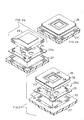
- an isometric view of the assembly in Figure 3 shows chip well 35 on the chip carrier.
- the chip carrier 26 may have corner placement notches 32 or a cutoff corner(s) indicated by reference numeral 33. Edges 34 may be in registry with appropriate assembly jigs for the device 25a, as well as the PCB 27 so that a precise registry of the metallization on the PCB 27 and the chip carrier 26 may be achieved.
- Chip carrier pads 53 and printed circuit board pads 30 must align through the solder columns 31. This alignment and position must be maintained during the assembly and soldering operation. If slight misalignment occurs, the wetting characteristics of the columns 31, along with pads 30 and 53, will caused the melted solder with its inherent surface tensions to effectively attach the columns to the pads with good solder fillet characteristics.
- Appropriate corner registry may be achieved such as by also providing a cut corner shown in a dashed line for the device in Figure 3 as 33a.
- each of the solder columns 31 shown in Figure 3 represents one embodiment of a particular solder column type.
- column 31 is shown in greater detail.
- the plate 25 has been positioned in a specific relationship with respect to the solder column 31.
- Locking collar 36 identified by the upper fillets 36a and lower fillets 36b are an important element in the device 25a. These locking collars 36 assure and provide for a number of advantages over the prior art devices known to the Applicants. Thus, the locking collar 36 and the plate 25 cooperate to assure appropriate coplanarity between the upper and lower column surfaces 31c and 31d, respectively.
- These surfaces 31c and 31d must be substantially parallel, must maintain this parallelism or coplanarity for the entire assembly during the production assembly and must not undergo change during the soldering stage of the process.
- the coplanarity must furthermore be substantially identical for each of the surfaces, namely surfaces 31c and 31d, and for each of the solder columns 31.
- the columns 31 must have substantially the same metallurgical behavior before soldering and after soldering.
- the coplanarity must be such that it is not rigidly maintained by the plate 25, but the plate may accommodate imposed stresses with compliancy also contributed by the relative movement of a solder column 31 in the neck area 36d, as well as at the additional lengths thereof.
- the solder filleting 57 and 56 (shown in Figure 8) at the top and bottom, respectively, provides additional column rigidity.
- the column may only be from about 0.12 inches (3.048 mm) to considerably shorter column height, such as down to 0.050 inches (1.270 mm). Shorter columns 31 are possible due to the improved compliancy characteristics of these, but for the reasons further discussed herein, it has been found that an appropriate column height such as 0.080 inches (2.032 mm) functions outstandingly well.
- the column height as shown in Figure 3a may be symmetrical along the long axis or along the centerline of plate 25, but other configurations are possible and have also been provided herein.
- the columns 31 which are traditionally around the periphery thereof may further be supplemented by interior grid-like array of additional columns serving same or different purposes.
- the columns 37 which may be of larger and smaller diameter as the column 31 shown in Figure 3a, may be for the purpose of heat dissipation. These columns have been shown in a grid pattern of nine, but the entire area may be of fewer, but larger, columns.
- the interior columns 37 may also facilitate assembly of the device.
- the lightening holes 15 which have also been shown in the top view in Figure 4 provide access during the flux removal operation and serve other purposes such as heat dissipation by convection cooling. Additional heat dissipation, as it is well known, is achieved by providing heat sink devices connected to interior columns 37, and these induce the heat transfer more readily in the space between the chip carrier 26 and the plate 25 and the printed circuit board 27 and the plate 25 again.
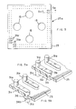
- FIG. 5 Another embodiment of the plate configuration with different solder columns is shown in Figure 5.
- Each of the columns in Figure 5 have been identified as 31a, and these, however, have further configurational variations.
- a view along line 5a in Figure 5 depicts this embodiment in Figure 5a.
- the plate 25 supports each of the columns in a different fashion to provide greater movement in all three principal directions (x, y, z), i.e., with a second column 31b and members 31e.
- the added flexibility and compliancy is thus assured for the especially troublesome temperature cycling conditions which may be encountered with devices such as, for example, found in the automotive field where the impedance considerations are not as critical.
- the embodiment shown in Figure 5b is considered to be more suitable.
- a locking collar 36 is provided for the device shown in Figure 5b. This locking collar resembles the locking collar shown in Figure 3a. It is, again, provided with fillets 36b and thus secures appropriately in the plate 25 the staggered column embodiment shown in Figure 5b.
- the plate 25 in accordance with the present invention, has a two-fold function. One, it secures in a coplanar relationship the vertical interconnection columns 31. Another function is for the plate 25 to act as a casting surface so that the microcasting technique uses the plate 25 as part of the mold die. If the plate were of a soft, elastic material, e.g., foam, or would be easily distortable, the coplanarity may not be as easily maintained after the casting operation has been completed.
- the total dimensions for these columns are typically dictated by the spacing of the array around the periphery thereof.
- Embodiments such as shown in Figure 5a and Figure 5b are more suitable for the peripheral placement of any number of pads.
- Embodiments such as 3a are, however, more suited for greater number of pads and closer arrays.
- the entire plate 25 it is also possible for the entire plate 25 to be arranged in an appropriate grid configuration such as illustrated by the small grid shown as solder posts 37 in Figure 4.
- solder column castings which can be achieved and are shown by the three embodiments shown in Figures 3a, 5a and 5b are only for purposes of illustration.
- the solder interconnection casting is made possible by the plate and die rigidity in a combination which maintains true coplanarity; not only between the upper and lower surfaces of columns 31 in the compliant interconnection device 25a, but also a true verticality for each of the individual microinterconnections around the periphery of the device.
- the present device lends itself admirably to interconnect chip carriers with the printed circuit boards.
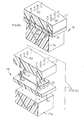
- the casting die 16 consists such as of a top plate 17 and a bottom plate 51 resting on a heated nozzle 17a which maintains the metal in a liquidus condition.
- the molten metal nozzle 17a has a heater (not shown). It maintains the metal at a temperature such that the metal can be extruded through and simultaneously via each of the individual solder cast column conduits or passages 50c corresponding to the number of solder columns 31 of dimensions which have been prepunched in an appropriate size and shape in the plate 25.
- the cross section of the molten metal nozzle conduit 50c illustrated in Figure 6 is identical or different.
- the dies 17, 51 and 17a resemble, in a top view, a plate 25 such as shown in Figure 4 or Figure 5 with the columns being, respectively, such as shown in Figures 3a, 5a or 5b.
- each of the solder columns' heicht is maintained for the desired length thereof by ejector pins 50.
- the metal flow distance is generally identical from the nozzle to all of the pins.
- individual length adjustment for each of the columns is also possible.
- the molten metal is being maintained in the molten metal reservoir at a high temperature such as 750° Fahrenheit, but the nozzle for the heater is maintained at a lower temperature or at or slightly above the metal melt temperature. This temperature condition has a two-fold function. One, the molten metal always works against a pressure gradient, and two, the solidification takes place rapidly.
- Suitable injection pressure is achieved such as by a hydraulic ram, not shown, which exerts its pressure on the molten metal reservoir 18 shown in Figure 1.
- a hydraulic ram not shown, which exerts its pressure on the molten metal reservoir 18 shown in Figure 1.
- the metal as it is being forced through the nozzle conduits 50c, while it is in a fairly hot state, is typically in a barely liquidus region when referring to a phase diagram.
- the ejector pins have terminated the metal movement with the locking collars 36 having been formed.
- the ejector half of the die 17 maintains a pin array by appropriate means so that all of the coplanarity is being maintained between the bottom plate and the top of the pin column.
- the bottom plate of the die 51 is typically at a lower temperature than the nozzle 17a, and thus assures, due to its relatively larger size and the air space 51a, an insulatipn sufficient to achieve at the same time fairly rapid chilling of the columns 31.
- the ejector plate 17 is split in half to form first die section 52 and second die section 53.
- the ejector pins 50 then function ir a different manner. These pins 50 in the first part of the operation are raised so that the metal can form a heated riser of sufficient height aliowing also for some venting capability should such be needed.
- the first die section 52 shown in Figure 6a by phantom lines, is held relatively rigid vis-a-vis the second die section 53.
- the height of the columns 31 is established by the second die section 53 first being moved relatively to the first die section 52, shearing off the risers 50e.
- a second die section (not shown) is placed in a corresponding position to the plate 17 with ejector pins 50, being now in position to eject each of the columns 31, after the bottom plate 51 shears off the bottom of the pins 31 as shown in Figure 6b.
- the ejector pins 50 eject the columns 31 as it is shown in Figure 6c.
- FIGs 6 to 6c illustrate the steps in which coplanarity may be achieved by the two different methods. As shown schematically in Figures 6 to 6c, the relative shearing motion on these microcolumns at the hot metal temperature is relatively easily accomplished with true coplanarity still being maintained.
- these die plates 17, 51 and 52 and nozzle conduits 50c are appropriately maintained so as to assure the proper operation of the casting procedure. For each of the selected solder alloys, these temperatures are established relative to each other.
- the device 25a as affixed to the chip carrier 26 and printed circuit hoard 27 and as used in service is illustrated by that Figure.
- Figure 8 in conjunction with Figure 13 shows the actual soldering process.
- the interconnection column 31 is cast from a lead-tin alloy composition having 95 percent lead and 5 percent tin.
- the melting point of that composition is in the vicinity of 327 degrees Celsius. At that temperature, tin-lead solder alloy is solid. At 327 degrees Celsius, 100 percent lead composition is liquid.
- a slight change in temperature and/or alloy composition will place the solder alloy in a liquidus or solidus condition.
- the liquidus condition is also called a "pasty" condition, i.e., where solid and liquid phases coexist. These have been indicated on the tin-lead phase diagram as the "pasty" region.
- the liquid temperature of the alloy is about 183 degrees Celsius. Consequently, a spread of 144 degrees Celsius in the respective melting points of the alloy from which the column 31 is formed and at which a eutectic mixture of a solder used is available for the soldering operation.
- FC-70 VPRS reflow solder system
- FC-70 VPRS reflow solder system
- solder reflow method lends itself to the melting of a solder alloy which is deposited on the solder column 31 in whatever form it is found to be most advantageous.
- the solder alloy may be deposited as a paste either admixed v:ith the flux or the flux may be separately deposited such as on the chip carrier !eads 53 or the printed circuit metallized part 30.
- the plate 25 also maintains the columns in a rigid position as a result of the collar lock 36.
- this assembly may then easily be baked so as to secure it further and maintain the rigidity of the structure. This baking drives off any volatiles from the solder paste and causes it to change to a cement-like material,
- the entire structure is placed in the vapor solder reflow chamber where the assembly is brought up to the thermal conditions necessary for reflowing the solder paste and forming the properly adhering structure between the feadless chip carrier 26 and the printed circuit board 27 via the compliant interconnection device 25a.
- solder cap 60 shown in Figure 9 aids in establishing different fillet configurations or different material flow properties based on the surface tension and remelt temperature considerations of a particular alloy or paste or alloy combinations. These are dependent upon the alloy content and the alloy additives.
- solder caps 60 may be placed on one or both ends of the solder column 31 and, if step-wise assembly at different temperatures is sought, such step-wise assembly may be achieved first by soldering to the printed circuit board a solder cap 60 reflowing at a higher temperature and thereafter placing the chip carrier on top thereof and reflowing solder at a lower solder alloy temperature.
- solder caps 60 of various compositions may easily be placed on the individual columns from a die machine or even by reflowing in a die set-up (not shown).
- the gravure deposition method provides for control, not only based on the size of the hole, depth thereof and viscosity of the paste, but also the paste might be transferred under hot conditions.
- the PCB 27 and the chip carrier 26 metallization pads 30 and 53, respectively, may also, by silk-screen printing, be treated only with flux. Flux removal is also one of the important aspects of the present invention. Because of the choice for the spacing and length for each of the individual columns 31, as well as the plate configuration, each of the devices 25a may be appropriately designed. Flux removal, after soldering, thereby does not present a problem. Flux control is especially troublesome as flux migration is affected by humidity. Shorting of the circuits is an ever-present problem due to flux contamination. In accordance with the present invention, the device 25a lends itself admirably to the flux removal because its interconnect space, such as .070 inches (1.778 mm), is sufficient to allow facile conventional washing and solvent intrusion and exit with the contaminants.
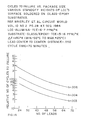
- FIG 14 this Figure illustrates the typical test used in the art where cycles to failure are measured as it concerns number of leads for each of the package anc, the stand-off distance.
- the cycle time is defined as being the totai of seventy minutes of which a prescribed time, as shown in the previously mentioned article by Luke et al, defines the various time periods.
- a prescribed time as shown in the previously mentioned article by Luke et al.
- the failures associated with the thermal and mechanically induced fatigue strains in the solder joints are a severe problem for large leadless ceramic chip carriers. These problems become especially severe when the chip carriers are thereafter joined to the printed circuit board having a different thermal coefficient of expansion. Moreover, the low yield points of tin-lead solder alloys when temperature cycled cause the solder joints to be subjected to plastic strain.
- the present device is, therefore, provided to accommodate the combination of strains encountered in large leadless chip carriers which are mounted on a printed circuit board having a different thermal coefficient cf expansion.
- solder volume is not necessary to achieve the connections as long as the appropriate coplanarity and vertical placement of the solder column to be joined, such as 31, is maintained with proper fillet formation achieved by proper deposition of solder paste or solder caps and proper flux removal.
- the joining techniques also lend themselves to rapid solidification rates because the amount of thermal mass involved in the typical soldering operation such as shown herein can be readily controlled by fast chilling. Hence, proper metallurgical practice may also be readily followed.
- microcast columns e.g., 31, are cast at a fairly high cycle rate in a continuous operation.
- the assembly of the chip carrier with the device may also be done with great reliability. It is especially noteworthy that the improvement can be achieved mounting these carriers with tighter lead spacing such as from 0.50 inches (1.270 mm) and even down to 0.20 inches (0.508 mm) centerline lead spacings.
- the device of .030 inch (0.762 mm) gap height has provided, in the present configuration with plate 25 present, generous space for cleaning and rinsing these solder joined assemblies. Even smaller gaps are believed to be sufficient to obtain the precision cleaning necessary in these devices.
- the support plate 25 onto which the solder columns are cast is generally of a dielectric nature equivalent to at least a clay-coated paper.
- the dielectric nature of the rlate must be maintained so as to obtain the electrical integritv of each of the solder columns during the operation of the device.
- the plate 25 material therefore, must aiso be compatible with the casting and reflow soldering temperatures and techniques and inert to the board cleaning solvents. Moreover, it must be capable of being cleanly punched so as to obtain the necessary definition for the whole pattern and at the same time have a relatively rigid structure to obtain the needed coplanarity.
Landscapes
- Engineering & Computer Science (AREA)
- Manufacturing & Machinery (AREA)
- Microelectronics & Electronic Packaging (AREA)
- Multi-Conductor Connections (AREA)
- Electric Connection Of Electric Components To Printed Circuits (AREA)
Applications Claiming Priority (4)
| Application Number | Priority Date | Filing Date | Title |
|---|---|---|---|
| US57510084A | 1984-01-30 | 1984-01-30 | |
| US575100 | 1984-01-30 | ||
| US67136584A | 1984-11-14 | 1984-11-14 | |
| US671365 | 1984-11-14 |
Publications (2)
| Publication Number | Publication Date |
|---|---|
| EP0150928A2 true EP0150928A2 (de) | 1985-08-07 |
| EP0150928A3 EP0150928A3 (de) | 1985-08-28 |
Family
ID=27076577
Family Applications (1)
| Application Number | Title | Priority Date | Filing Date |
|---|---|---|---|
| EP85300149A Withdrawn EP0150928A3 (de) | 1984-01-30 | 1985-01-09 | Anpassbare Zwischenverbindungsvorrichtung und Zusammenbau, Verfahren zum Herstellen und Giessen einer Mikrozwischenverbindung |
Country Status (1)
| Country | Link |
|---|---|
| EP (1) | EP0150928A3 (de) |
Cited By (4)
| Publication number | Priority date | Publication date | Assignee | Title |
|---|---|---|---|---|
| US4927697A (en) * | 1987-11-28 | 1990-05-22 | British Aerospace Public Limited Company | Surface mounting leadless components on conductor pattern supporting substrates |
| EP0396522A3 (de) * | 1989-05-05 | 1992-01-22 | International Business Machines Corporation | Universelle Anordnung für elektrische Zwischenverbindungen und Herstellungsverfahren dafür |
| EP0804056A3 (de) * | 1996-04-26 | 1999-02-03 | NGK Spark Plug Co. Ltd. | Verbesserungen bezüglich einer Verbindungsplatte |
| EP0804057A3 (de) * | 1996-04-26 | 1999-02-10 | NGK Spark Plug Co. Ltd. | Verbesserungen bezüglich einer Verbindungsplatte zur Verbindung zwischen einer Grundplatte und einer Montierungsplatte |
Family Cites Families (5)
| Publication number | Priority date | Publication date | Assignee | Title |
|---|---|---|---|---|
| DE1919567A1 (de) * | 1969-04-17 | 1970-11-05 | Siemens Ag | Loesbare elektrische Verbindungen zwischen Mikrobaugruppen und oder Verdrahtungsplatten |
| US4179802A (en) * | 1978-03-27 | 1979-12-25 | International Business Machines Corporation | Studded chip attachment process |
| US4390220A (en) * | 1981-04-02 | 1983-06-28 | Burroughs Corporation | Electrical connector assembly for an integrated circuit package |
| US4413308A (en) * | 1981-08-31 | 1983-11-01 | Bell Telephone Laboratories, Incorporated | Printed wiring board construction |
| US4412642A (en) * | 1982-03-15 | 1983-11-01 | Western Electric Co., Inc. | Cast solder leads for leadless semiconductor circuits |
-
1985
- 1985-01-09 EP EP85300149A patent/EP0150928A3/de not_active Withdrawn
Cited By (8)
| Publication number | Priority date | Publication date | Assignee | Title |
|---|---|---|---|---|
| US4927697A (en) * | 1987-11-28 | 1990-05-22 | British Aerospace Public Limited Company | Surface mounting leadless components on conductor pattern supporting substrates |
| EP0396522A3 (de) * | 1989-05-05 | 1992-01-22 | International Business Machines Corporation | Universelle Anordnung für elektrische Zwischenverbindungen und Herstellungsverfahren dafür |
| EP0804056A3 (de) * | 1996-04-26 | 1999-02-03 | NGK Spark Plug Co. Ltd. | Verbesserungen bezüglich einer Verbindungsplatte |
| EP0804057A3 (de) * | 1996-04-26 | 1999-02-10 | NGK Spark Plug Co. Ltd. | Verbesserungen bezüglich einer Verbindungsplatte zur Verbindung zwischen einer Grundplatte und einer Montierungsplatte |
| US6080936A (en) * | 1996-04-26 | 2000-06-27 | Ngk Spark Plug Co., Ltd. | Connecting board with oval-shaped protrusions |
| US6148900A (en) * | 1996-04-26 | 2000-11-21 | Ngk Spark Plug Co., Ltd. | Connecting board for connection between base plate and mounting board |
| KR100275432B1 (ko) * | 1996-04-26 | 2001-01-15 | 가나가와 시게노부 | 중계 기판의 제조 방법 |
| KR100275431B1 (ko) * | 1996-04-26 | 2001-01-15 | 가나가와 시게노부 | 중계 기판 |
Also Published As
| Publication number | Publication date |
|---|---|
| EP0150928A3 (de) | 1985-08-28 |
Similar Documents
| Publication | Publication Date | Title |
|---|---|---|
| CA2115553C (en) | Plated compliant lead | |
| CA1297203C (en) | Compliant s-leads for chip carriers | |
| KR910007103B1 (ko) | 도선형성 및 도선 없는 부품에 도선을 접착시키는 방법 | |
| US5783865A (en) | Wiring substrate and semiconductor device | |
| US5639696A (en) | Microelectronic integrated circuit mounted on circuit board with solder column grid array interconnection, and method of fabricating the solder column grid array | |
| US7125789B2 (en) | Composite metal column for mounting semiconductor device | |
| JPH06188355A (ja) | 電子相互接続の製作方法 | |
| US4554575A (en) | Low stress leadless chip carrier and method of assembly | |
| US4402450A (en) | Adapting contacts for connection thereto | |
| EP0242369B1 (de) | Integrierte schaltungspackungen für oberflächenmontierung mit löttragenden leitern | |
| US9865479B2 (en) | Method of attaching components to printed cirucuit board with reduced accumulated tolerances | |
| GB2138339A (en) | Applying and securing solder-coated or solderable spheres to solderable or solder-coated terminal pads | |
| EP0150928A2 (de) | Anpassbare Zwischenverbindungsvorrichtung und Zusammenbau, Verfahren zum Herstellen und Giessen einer Mikrozwischenverbindung | |
| US20160255728A1 (en) | Semiconductor package, electronic device, and solder mounting method | |
| US20070007323A1 (en) | Standoff structures for surface mount components | |
| Dudderar et al. | AT&T spl mu/Surface Mount Assembly: A New Technology for the Large Volume Fabrication of Cost Effective Flip-Chip MCMs | |
| US6853558B1 (en) | Surface mount power supply device and associated method | |
| EP0270820B1 (de) | Vorbereitung von Drahtadern eines oberflächenmontierbaren Bauteils | |
| JPH0550876B2 (de) | ||
| JPS63283147A (ja) | 半導体装置 | |
| JPH05206627A (ja) | リード接続用電極及びリード・電極の接続方法 | |
| JPS62263693A (ja) | 電子部品をプリント回路基板にはんだ付けする方法 | |
| GB2126014A (en) | Heat sink for electronic circuit assemblies | |
| JPH05102651A (ja) | 回路素子の表面実装方法 | |
| Cole et al. | Ceramic Ball and Column Grid Arrays |
Legal Events
| Date | Code | Title | Description |
|---|---|---|---|
| PUAI | Public reference made under article 153(3) epc to a published international application that has entered the european phase |
Free format text: ORIGINAL CODE: 0009012 |
|
| PUAL | Search report despatched |
Free format text: ORIGINAL CODE: 0009013 |
|
| AK | Designated contracting states |
Designated state(s): BE DE FR GB IT NL |
|
| AK | Designated contracting states |
Designated state(s): BE DE FR GB IT NL |
|
| STAA | Information on the status of an ep patent application or granted ep patent |
Free format text: STATUS: THE APPLICATION IS DEEMED TO BE WITHDRAWN |
|
| 18D | Application deemed to be withdrawn |
Effective date: 19860429 |
|
| RIN1 | Information on inventor provided before grant (corrected) |
Inventor name: PAUZA, WILLIAM VITO |