EP0151413A2 - Dépôt métallique sélectif sur une surface diélectrique - Google Patents
Dépôt métallique sélectif sur une surface diélectrique Download PDFInfo
- Publication number
- EP0151413A2 EP0151413A2 EP85100466A EP85100466A EP0151413A2 EP 0151413 A2 EP0151413 A2 EP 0151413A2 EP 85100466 A EP85100466 A EP 85100466A EP 85100466 A EP85100466 A EP 85100466A EP 0151413 A2 EP0151413 A2 EP 0151413A2
- Authority
- EP
- European Patent Office
- Prior art keywords
- dielectric surface
- areas
- metal
- solution
- selectively
- Prior art date
- Legal status (The legal status is an assumption and is not a legal conclusion. Google has not performed a legal analysis and makes no representation as to the accuracy of the status listed.)
- Withdrawn
Links
Images


Classifications
-
- C—CHEMISTRY; METALLURGY
- C23—COATING METALLIC MATERIAL; COATING MATERIAL WITH METALLIC MATERIAL; CHEMICAL SURFACE TREATMENT; DIFFUSION TREATMENT OF METALLIC MATERIAL; COATING BY VACUUM EVAPORATION, BY SPUTTERING, BY ION IMPLANTATION OR BY CHEMICAL VAPOUR DEPOSITION, IN GENERAL; INHIBITING CORROSION OF METALLIC MATERIAL OR INCRUSTATION IN GENERAL
- C23C—COATING METALLIC MATERIAL; COATING MATERIAL WITH METALLIC MATERIAL; SURFACE TREATMENT OF METALLIC MATERIAL BY DIFFUSION INTO THE SURFACE, BY CHEMICAL CONVERSION OR SUBSTITUTION; COATING BY VACUUM EVAPORATION, BY SPUTTERING, BY ION IMPLANTATION OR BY CHEMICAL VAPOUR DEPOSITION, IN GENERAL
- C23C18/00—Chemical coating by decomposition of either liquid compounds or solutions of the coating forming compounds, without leaving reaction products of surface material in the coating; Contact plating
- C23C18/16—Chemical coating by decomposition of either liquid compounds or solutions of the coating forming compounds, without leaving reaction products of surface material in the coating; Contact plating by reduction or substitution, e.g. electroless plating
- C23C18/1601—Process or apparatus
- C23C18/1603—Process or apparatus coating on selected surface areas
- C23C18/1607—Process or apparatus coating on selected surface areas by direct patterning
- C23C18/1608—Process or apparatus coating on selected surface areas by direct patterning from pretreatment step, i.e. selective pre-treatment
-
- C—CHEMISTRY; METALLURGY
- C23—COATING METALLIC MATERIAL; COATING MATERIAL WITH METALLIC MATERIAL; CHEMICAL SURFACE TREATMENT; DIFFUSION TREATMENT OF METALLIC MATERIAL; COATING BY VACUUM EVAPORATION, BY SPUTTERING, BY ION IMPLANTATION OR BY CHEMICAL VAPOUR DEPOSITION, IN GENERAL; INHIBITING CORROSION OF METALLIC MATERIAL OR INCRUSTATION IN GENERAL
- C23C—COATING METALLIC MATERIAL; COATING MATERIAL WITH METALLIC MATERIAL; SURFACE TREATMENT OF METALLIC MATERIAL BY DIFFUSION INTO THE SURFACE, BY CHEMICAL CONVERSION OR SUBSTITUTION; COATING BY VACUUM EVAPORATION, BY SPUTTERING, BY ION IMPLANTATION OR BY CHEMICAL VAPOUR DEPOSITION, IN GENERAL
- C23C18/00—Chemical coating by decomposition of either liquid compounds or solutions of the coating forming compounds, without leaving reaction products of surface material in the coating; Contact plating
- C23C18/16—Chemical coating by decomposition of either liquid compounds or solutions of the coating forming compounds, without leaving reaction products of surface material in the coating; Contact plating by reduction or substitution, e.g. electroless plating
- C23C18/1601—Process or apparatus
- C23C18/1603—Process or apparatus coating on selected surface areas
- C23C18/1607—Process or apparatus coating on selected surface areas by direct patterning
- C23C18/1612—Process or apparatus coating on selected surface areas by direct patterning through irradiation means
-
- C—CHEMISTRY; METALLURGY
- C23—COATING METALLIC MATERIAL; COATING MATERIAL WITH METALLIC MATERIAL; CHEMICAL SURFACE TREATMENT; DIFFUSION TREATMENT OF METALLIC MATERIAL; COATING BY VACUUM EVAPORATION, BY SPUTTERING, BY ION IMPLANTATION OR BY CHEMICAL VAPOUR DEPOSITION, IN GENERAL; INHIBITING CORROSION OF METALLIC MATERIAL OR INCRUSTATION IN GENERAL
- C23C—COATING METALLIC MATERIAL; COATING MATERIAL WITH METALLIC MATERIAL; SURFACE TREATMENT OF METALLIC MATERIAL BY DIFFUSION INTO THE SURFACE, BY CHEMICAL CONVERSION OR SUBSTITUTION; COATING BY VACUUM EVAPORATION, BY SPUTTERING, BY ION IMPLANTATION OR BY CHEMICAL VAPOUR DEPOSITION, IN GENERAL
- C23C18/00—Chemical coating by decomposition of either liquid compounds or solutions of the coating forming compounds, without leaving reaction products of surface material in the coating; Contact plating
- C23C18/16—Chemical coating by decomposition of either liquid compounds or solutions of the coating forming compounds, without leaving reaction products of surface material in the coating; Contact plating by reduction or substitution, e.g. electroless plating
- C23C18/18—Pretreatment of the material to be coated
- C23C18/1851—Pretreatment of the material to be coated of surfaces of non-metallic or semiconducting in organic material
- C23C18/1855—Pretreatment of the material to be coated of surfaces of non-metallic or semiconducting in organic material by mechanical pretreatment, e.g. grinding, sanding
-
- C—CHEMISTRY; METALLURGY
- C23—COATING METALLIC MATERIAL; COATING MATERIAL WITH METALLIC MATERIAL; CHEMICAL SURFACE TREATMENT; DIFFUSION TREATMENT OF METALLIC MATERIAL; COATING BY VACUUM EVAPORATION, BY SPUTTERING, BY ION IMPLANTATION OR BY CHEMICAL VAPOUR DEPOSITION, IN GENERAL; INHIBITING CORROSION OF METALLIC MATERIAL OR INCRUSTATION IN GENERAL
- C23C—COATING METALLIC MATERIAL; COATING MATERIAL WITH METALLIC MATERIAL; SURFACE TREATMENT OF METALLIC MATERIAL BY DIFFUSION INTO THE SURFACE, BY CHEMICAL CONVERSION OR SUBSTITUTION; COATING BY VACUUM EVAPORATION, BY SPUTTERING, BY ION IMPLANTATION OR BY CHEMICAL VAPOUR DEPOSITION, IN GENERAL
- C23C18/00—Chemical coating by decomposition of either liquid compounds or solutions of the coating forming compounds, without leaving reaction products of surface material in the coating; Contact plating
- C23C18/16—Chemical coating by decomposition of either liquid compounds or solutions of the coating forming compounds, without leaving reaction products of surface material in the coating; Contact plating by reduction or substitution, e.g. electroless plating
- C23C18/18—Pretreatment of the material to be coated
- C23C18/1851—Pretreatment of the material to be coated of surfaces of non-metallic or semiconducting in organic material
- C23C18/1862—Pretreatment of the material to be coated of surfaces of non-metallic or semiconducting in organic material by radiant energy
- C23C18/1868—Radiation, e.g. UV, laser
-
- C—CHEMISTRY; METALLURGY
- C23—COATING METALLIC MATERIAL; COATING MATERIAL WITH METALLIC MATERIAL; CHEMICAL SURFACE TREATMENT; DIFFUSION TREATMENT OF METALLIC MATERIAL; COATING BY VACUUM EVAPORATION, BY SPUTTERING, BY ION IMPLANTATION OR BY CHEMICAL VAPOUR DEPOSITION, IN GENERAL; INHIBITING CORROSION OF METALLIC MATERIAL OR INCRUSTATION IN GENERAL
- C23C—COATING METALLIC MATERIAL; COATING MATERIAL WITH METALLIC MATERIAL; SURFACE TREATMENT OF METALLIC MATERIAL BY DIFFUSION INTO THE SURFACE, BY CHEMICAL CONVERSION OR SUBSTITUTION; COATING BY VACUUM EVAPORATION, BY SPUTTERING, BY ION IMPLANTATION OR BY CHEMICAL VAPOUR DEPOSITION, IN GENERAL
- C23C18/00—Chemical coating by decomposition of either liquid compounds or solutions of the coating forming compounds, without leaving reaction products of surface material in the coating; Contact plating
- C23C18/16—Chemical coating by decomposition of either liquid compounds or solutions of the coating forming compounds, without leaving reaction products of surface material in the coating; Contact plating by reduction or substitution, e.g. electroless plating
- C23C18/18—Pretreatment of the material to be coated
- C23C18/1851—Pretreatment of the material to be coated of surfaces of non-metallic or semiconducting in organic material
- C23C18/1872—Pretreatment of the material to be coated of surfaces of non-metallic or semiconducting in organic material by chemical pretreatment
- C23C18/1875—Pretreatment of the material to be coated of surfaces of non-metallic or semiconducting in organic material by chemical pretreatment only one step pretreatment
- C23C18/1879—Use of metal, e.g. activation, sensitisation with noble metals
-
- C—CHEMISTRY; METALLURGY
- C23—COATING METALLIC MATERIAL; COATING MATERIAL WITH METALLIC MATERIAL; CHEMICAL SURFACE TREATMENT; DIFFUSION TREATMENT OF METALLIC MATERIAL; COATING BY VACUUM EVAPORATION, BY SPUTTERING, BY ION IMPLANTATION OR BY CHEMICAL VAPOUR DEPOSITION, IN GENERAL; INHIBITING CORROSION OF METALLIC MATERIAL OR INCRUSTATION IN GENERAL
- C23C—COATING METALLIC MATERIAL; COATING MATERIAL WITH METALLIC MATERIAL; SURFACE TREATMENT OF METALLIC MATERIAL BY DIFFUSION INTO THE SURFACE, BY CHEMICAL CONVERSION OR SUBSTITUTION; COATING BY VACUUM EVAPORATION, BY SPUTTERING, BY ION IMPLANTATION OR BY CHEMICAL VAPOUR DEPOSITION, IN GENERAL
- C23C18/00—Chemical coating by decomposition of either liquid compounds or solutions of the coating forming compounds, without leaving reaction products of surface material in the coating; Contact plating
- C23C18/16—Chemical coating by decomposition of either liquid compounds or solutions of the coating forming compounds, without leaving reaction products of surface material in the coating; Contact plating by reduction or substitution, e.g. electroless plating
- C23C18/18—Pretreatment of the material to be coated
- C23C18/20—Pretreatment of the material to be coated of organic surfaces, e.g. resins
- C23C18/2006—Pretreatment of the material to be coated of organic surfaces, e.g. resins by other methods than those of C23C18/22 - C23C18/30
- C23C18/2013—Pretreatment of the material to be coated of organic surfaces, e.g. resins by other methods than those of C23C18/22 - C23C18/30 by mechanical pretreatment, e.g. grinding, sanding
-
- C—CHEMISTRY; METALLURGY
- C23—COATING METALLIC MATERIAL; COATING MATERIAL WITH METALLIC MATERIAL; CHEMICAL SURFACE TREATMENT; DIFFUSION TREATMENT OF METALLIC MATERIAL; COATING BY VACUUM EVAPORATION, BY SPUTTERING, BY ION IMPLANTATION OR BY CHEMICAL VAPOUR DEPOSITION, IN GENERAL; INHIBITING CORROSION OF METALLIC MATERIAL OR INCRUSTATION IN GENERAL
- C23C—COATING METALLIC MATERIAL; COATING MATERIAL WITH METALLIC MATERIAL; SURFACE TREATMENT OF METALLIC MATERIAL BY DIFFUSION INTO THE SURFACE, BY CHEMICAL CONVERSION OR SUBSTITUTION; COATING BY VACUUM EVAPORATION, BY SPUTTERING, BY ION IMPLANTATION OR BY CHEMICAL VAPOUR DEPOSITION, IN GENERAL
- C23C18/00—Chemical coating by decomposition of either liquid compounds or solutions of the coating forming compounds, without leaving reaction products of surface material in the coating; Contact plating
- C23C18/16—Chemical coating by decomposition of either liquid compounds or solutions of the coating forming compounds, without leaving reaction products of surface material in the coating; Contact plating by reduction or substitution, e.g. electroless plating
- C23C18/18—Pretreatment of the material to be coated
- C23C18/20—Pretreatment of the material to be coated of organic surfaces, e.g. resins
- C23C18/2006—Pretreatment of the material to be coated of organic surfaces, e.g. resins by other methods than those of C23C18/22 - C23C18/30
- C23C18/2026—Pretreatment of the material to be coated of organic surfaces, e.g. resins by other methods than those of C23C18/22 - C23C18/30 by radiant energy
- C23C18/204—Radiation, e.g. UV, laser
-
- C—CHEMISTRY; METALLURGY
- C23—COATING METALLIC MATERIAL; COATING MATERIAL WITH METALLIC MATERIAL; CHEMICAL SURFACE TREATMENT; DIFFUSION TREATMENT OF METALLIC MATERIAL; COATING BY VACUUM EVAPORATION, BY SPUTTERING, BY ION IMPLANTATION OR BY CHEMICAL VAPOUR DEPOSITION, IN GENERAL; INHIBITING CORROSION OF METALLIC MATERIAL OR INCRUSTATION IN GENERAL
- C23C—COATING METALLIC MATERIAL; COATING MATERIAL WITH METALLIC MATERIAL; SURFACE TREATMENT OF METALLIC MATERIAL BY DIFFUSION INTO THE SURFACE, BY CHEMICAL CONVERSION OR SUBSTITUTION; COATING BY VACUUM EVAPORATION, BY SPUTTERING, BY ION IMPLANTATION OR BY CHEMICAL VAPOUR DEPOSITION, IN GENERAL
- C23C18/00—Chemical coating by decomposition of either liquid compounds or solutions of the coating forming compounds, without leaving reaction products of surface material in the coating; Contact plating
- C23C18/16—Chemical coating by decomposition of either liquid compounds or solutions of the coating forming compounds, without leaving reaction products of surface material in the coating; Contact plating by reduction or substitution, e.g. electroless plating
- C23C18/18—Pretreatment of the material to be coated
- C23C18/20—Pretreatment of the material to be coated of organic surfaces, e.g. resins
- C23C18/28—Sensitising or activating
- C23C18/30—Activating or accelerating or sensitising with palladium or other noble metal
-
- C—CHEMISTRY; METALLURGY
- C23—COATING METALLIC MATERIAL; COATING MATERIAL WITH METALLIC MATERIAL; CHEMICAL SURFACE TREATMENT; DIFFUSION TREATMENT OF METALLIC MATERIAL; COATING BY VACUUM EVAPORATION, BY SPUTTERING, BY ION IMPLANTATION OR BY CHEMICAL VAPOUR DEPOSITION, IN GENERAL; INHIBITING CORROSION OF METALLIC MATERIAL OR INCRUSTATION IN GENERAL
- C23C—COATING METALLIC MATERIAL; COATING MATERIAL WITH METALLIC MATERIAL; SURFACE TREATMENT OF METALLIC MATERIAL BY DIFFUSION INTO THE SURFACE, BY CHEMICAL CONVERSION OR SUBSTITUTION; COATING BY VACUUM EVAPORATION, BY SPUTTERING, BY ION IMPLANTATION OR BY CHEMICAL VAPOUR DEPOSITION, IN GENERAL
- C23C18/00—Chemical coating by decomposition of either liquid compounds or solutions of the coating forming compounds, without leaving reaction products of surface material in the coating; Contact plating
- C23C18/16—Chemical coating by decomposition of either liquid compounds or solutions of the coating forming compounds, without leaving reaction products of surface material in the coating; Contact plating by reduction or substitution, e.g. electroless plating
- C23C18/31—Coating with metals
- C23C18/32—Coating with nickel, cobalt or mixtures thereof with phosphorus or boron
- C23C18/34—Coating with nickel, cobalt or mixtures thereof with phosphorus or boron using reducing agents
-
- C—CHEMISTRY; METALLURGY
- C23—COATING METALLIC MATERIAL; COATING MATERIAL WITH METALLIC MATERIAL; CHEMICAL SURFACE TREATMENT; DIFFUSION TREATMENT OF METALLIC MATERIAL; COATING BY VACUUM EVAPORATION, BY SPUTTERING, BY ION IMPLANTATION OR BY CHEMICAL VAPOUR DEPOSITION, IN GENERAL; INHIBITING CORROSION OF METALLIC MATERIAL OR INCRUSTATION IN GENERAL
- C23C—COATING METALLIC MATERIAL; COATING MATERIAL WITH METALLIC MATERIAL; SURFACE TREATMENT OF METALLIC MATERIAL BY DIFFUSION INTO THE SURFACE, BY CHEMICAL CONVERSION OR SUBSTITUTION; COATING BY VACUUM EVAPORATION, BY SPUTTERING, BY ION IMPLANTATION OR BY CHEMICAL VAPOUR DEPOSITION, IN GENERAL
- C23C18/00—Chemical coating by decomposition of either liquid compounds or solutions of the coating forming compounds, without leaving reaction products of surface material in the coating; Contact plating
- C23C18/16—Chemical coating by decomposition of either liquid compounds or solutions of the coating forming compounds, without leaving reaction products of surface material in the coating; Contact plating by reduction or substitution, e.g. electroless plating
- C23C18/31—Coating with metals
- C23C18/38—Coating with copper
- C23C18/40—Coating with copper using reducing agents
- C23C18/405—Formaldehyde
-
- H—ELECTRICITY
- H05—ELECTRIC TECHNIQUES NOT OTHERWISE PROVIDED FOR
- H05K—PRINTED CIRCUITS; CASINGS OR CONSTRUCTIONAL DETAILS OF ELECTRIC APPARATUS; MANUFACTURE OF ASSEMBLAGES OF ELECTRICAL COMPONENTS
- H05K3/00—Apparatus or processes for manufacturing printed circuits
- H05K3/10—Apparatus or processes for manufacturing printed circuits in which conductive material is applied to the insulating support in such a manner as to form the desired conductive pattern
- H05K3/18—Apparatus or processes for manufacturing printed circuits in which conductive material is applied to the insulating support in such a manner as to form the desired conductive pattern using precipitation techniques to apply the conductive material
- H05K3/181—Apparatus or processes for manufacturing printed circuits in which conductive material is applied to the insulating support in such a manner as to form the desired conductive pattern using precipitation techniques to apply the conductive material by electroless plating
- H05K3/182—Apparatus or processes for manufacturing printed circuits in which conductive material is applied to the insulating support in such a manner as to form the desired conductive pattern using precipitation techniques to apply the conductive material by electroless plating characterised by the patterning method
- H05K3/185—Apparatus or processes for manufacturing printed circuits in which conductive material is applied to the insulating support in such a manner as to form the desired conductive pattern using precipitation techniques to apply the conductive material by electroless plating characterised by the patterning method by making a catalytic pattern by photo-imaging
-
- C—CHEMISTRY; METALLURGY
- C23—COATING METALLIC MATERIAL; COATING MATERIAL WITH METALLIC MATERIAL; CHEMICAL SURFACE TREATMENT; DIFFUSION TREATMENT OF METALLIC MATERIAL; COATING BY VACUUM EVAPORATION, BY SPUTTERING, BY ION IMPLANTATION OR BY CHEMICAL VAPOUR DEPOSITION, IN GENERAL; INHIBITING CORROSION OF METALLIC MATERIAL OR INCRUSTATION IN GENERAL
- C23C—COATING METALLIC MATERIAL; COATING MATERIAL WITH METALLIC MATERIAL; SURFACE TREATMENT OF METALLIC MATERIAL BY DIFFUSION INTO THE SURFACE, BY CHEMICAL CONVERSION OR SUBSTITUTION; COATING BY VACUUM EVAPORATION, BY SPUTTERING, BY ION IMPLANTATION OR BY CHEMICAL VAPOUR DEPOSITION, IN GENERAL
- C23C18/00—Chemical coating by decomposition of either liquid compounds or solutions of the coating forming compounds, without leaving reaction products of surface material in the coating; Contact plating
- C23C18/16—Chemical coating by decomposition of either liquid compounds or solutions of the coating forming compounds, without leaving reaction products of surface material in the coating; Contact plating by reduction or substitution, e.g. electroless plating
- C23C18/1601—Process or apparatus
- C23C18/1633—Process of electroless plating
- C23C18/1646—Characteristics of the product obtained
- C23C18/165—Multilayered product
- C23C18/1653—Two or more layers with at least one layer obtained by electroless plating and one layer obtained by electroplating
Definitions
- the present invention relates to selective or pattern plating on a dielectric substrate such as plastic, glass, synthetic resin or ceramic. More particularly, the invention relates to a method of plating a pattern of metal on a dielectric surface by utilizing selective but maskless chemical or electroless metal deposition.
- patterned or selective metal plating can be achieved by chemical or electroless (two terms are interchangeably used in the art) metal deposition in which masking is employed to delineate the patterns. While masking plating techniques provide finely delineated patterns of metal which are now extensively needed in the manufacture of, for example, electronic circuits on dielectric substrates, these processes are inefficient and costly. Besides they may impose serious restriction on the size of the pattern which can be batch-deposited.
- the plating substrate is a nickel film vapor-deposited on a glass workpiece.
- the argon laser beam is passed through a nickel electroless plating solution and illuminates selected regions of the surface of the nickel film in contact therewith.
- the beam alternatively is passed through both the solution and the glass base and illuminates the nickel-glass interface beneath such regions of the surface of the nickel film in contact with the nickel electroless plating solution.
- An object of the present invention is to establish a maskless selective plating method which allows a pattern of metal to be electrolessly plated directly on a dielectric substrate.
- Another object of the invention is to provide a method described which is capable of yielding high-resolution patterns of metal on a dielectric substrate or substrates at an enhanced plating rate or rate of yield.
- a method of plating a pattern of metal on a dielectric surface comprises the steps of: a) masklessly treating the dielectric surface to selectively activate preselected areas thereof so that the dielectric surface when in contact with a priming solution becomes catalytic, and thereby receptive to electroless metal deposition, selectively at said preselected areas; and b) contacting the treated dielectric surface with an electroless plating solution to allow metal therefrom to auto-reductively deposit selectively at said preselected, catalyzed areas, thereby forming the pattern of metal desired on the dielectric surface.
- the chemical or electroless plating process is generally divided into the main stage in which a substrate is brought into contact with an electroless'plating solution and the priming stage preliminary to the main stage.
- the dielectric substrate is brought into contact with a priming solution, e.g. a palladium-chloride solution and/or a stannous-chloride solution which catalyzes the substrate prior to the electroless metal deposition, thus providing catalytic (nucleating) sites on the substrate surface which sites are receptive to the electroless metal deposition thereon, or on which sites the metal can be auto-catalytically or -reductively deposited.
- a priming solution e.g. a palladium-chloride solution and/or a stannous-chloride solution which catalyzes the substrate prior to the electroless metal deposition, thus providing catalytic (nucleating) sites on the substrate surface which sites are receptive to the electroless metal deposition thereon, or on which sites the metal can be
- the selective plating method according to the present invention involves, as the step preliminary to the main, electroless plating step, the step of masklessly treating the dielectric surface to selectively activate preselected areas thereof so that the dielectric surface when in contact with the priming solution becomes catalytic, and thereby receptive to the electroless metal deposition, selectively at those preselected areas.
- the dielectric surface in the preliminary step is so treated as defined by exposing the dielectric surface to irradiation by an energy beam. This is in sharp contrast with the aforemen. tioned BLUM et al process in which an energy beam is employed to irradiate the area contacted by the electroless plating solution and which requires the preliminary vapor deposition (naturally non-localized or, if to be localized, with a masking) of the same metal to be electrolessly deposited.
- the energy beam is conveniently a focused beam of electromagnetic radiation and can be advantageously a laser beam, a beam of Xenon lamp, or a beam of microwaves (having a frequency in excess of 100 MHz/and preferably a frequency of 2678 MHz).
- the beam should have a power density in excess of 10 2 watts/cm 2 and preferably not less than 10 3 watts/cm 2 but not more than 10 watts/cm.
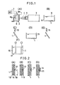
- a dielectric substrate 1 is shown as securely mounted on a vertical work support 2.
- a laser (e.g. argon laser) generator 3 produces a laser beam 4 focused through a lens system 5 to impinge on the surface of the dielectric substrate 1 with a power density of, e.g., 1. 5 x 10 3 watts/cm 2 and with a beam spot diameter of, e.g., 1 mm.
- the beam spot moves on the dielectric surface 3, leaving behind a sharply delineated beam-treated area (line) of a width of 1 mm.
- the laser generator 3 is fixed in position and the work support 2 is movably carried by a compound drive table 6 provided with a pair of motors Mx, My.
- the motors Mx and My are driven by drive command signals furnished from a numerical control (NC) unit 7 to displace the substrate in a vertical or X-Y plane so that the trajactory of the beam spot on the surface of the substrate 1 follows a predetermined path programmed in the NC unit 7 to precisely cover preselected areas thereon and delineate a predetermined pattern to be later electrolessly plated with metal.
- the dielectric substrate 1 and the beam 4 impinging thereon are placed in a vacuum or in a rarefied or otherwise clean atmosphere which may be filled with an inert gas.
- the substrate 1 prior to the beam treatment is washed with a neutral detergent, water-rinsed and.dried.
- the dielectric substrate 1 may, for example, be a composite plate which as shown in FIG. 2 comprises a glass-fiber woven textile 1A having layers 1B of an epoxy resin coated thereon at both sides.
- each site of the dielectric surface irradiated with the focused beam 4 is highly activated. Not only does the beam irradiation or bombardment heat or thermally activate the irradiated or bombarded site in the usual sense but apparently it effectively removes and strips away moisture, adsorptive gaseous particles, thin oxide films and other impurities normally firmly adherent to and coated on the substrate of a dielectric substrate 1 such as a ceramic, synthetic resin or the like. As a result, it appears that on each treated site there develops a "naked" surface of the substrate which surface is highly chemically unstable or "excited". Such an activated site as formed on the dielectric surface is diagrammatically illustrated at.10 in FIG. 2(A).
- the treated substrate 1 is introduced into and immersed in the bath 8 of a priming solution 9 as shown in FIG. 1(B).
- the substrate 1 in contact with the priming solution 9 (FIG. 2(B)) then becomes catalytic, and develops precipitation nuclei, selectively at the activated sites 10.
- Such nuclei of catalytic precipitation as formed and left after removal of the solution 9 by water rinse on the dielectric substrate 3 is diagrammatically shown at 11 in FIG. 2(C).
- the priming solution 9 may be a solution of palladium chloride and may be composed as tabulated in Table 1 below.
- the substrate 1 as shown in FIG. I(C) is washed with chloric acid (e.g. of a 10% concentration) and then water-rinsed.
- Nozzles 12 are used to deliver chloric acid flowing over the substrate 1 down to remove the adherent priming solution therefrom and then to deliver water flowing over the substrate 1 down to remove the chloric acid therefrom.
- the substrate 1 is introduced into and immersed in a bath of an electroless plating solution 13 as shown in FIG. 1 (D). This will cause metal (e.g. copper or nickel) from the electroless plating solution 13 to auto-reductively or -catalytically deposit selectively at an activated, preselected areas of the dielectric surface of the substrate 1.
- FIG. 2(D) shows the metal 14 depositing on the activation (palladium) nucleus 11.
- the solution 13 may be composed as tabulated in Table 2 below.
- the solution 13 may be composed as tabulated in Table 3 below.
- the substrate 1 After removal from the bath of the electroless plating solution 13, the substrate 1 is rinsed with water as shown in FIG. 1(E).
- a nozzle 15 is used to deliver water flowing over the substrate 1 down to remove the adherent electroless plating solution 13 therefrom.
- the substrate 1 may optionally be introduced into and immersed in a bath of an electrodepositing solution 16 as shown in FIG. 1(F).
- An anode 17 is juxtaposed with the substrate 1 as the cathode of the bath in the electroplating solution 16 and a direct current is passed between the anode 17 and the cathode to electrodeposite the metal (e.g. copper or nickel) from the solution 16 selectively onto the electrolessly metal-deposited areas to increase the thickness of metal plating.
- the metal e.g. copper or nickel
- the beam 4 can be displaced to trace the preselected areas at a rate of displacement as high as 180 m/min (3.0 m/sec) to enable the palladium nuclei 11 (FIG. 11) to be sufficiently formed selectively onto those areas of the substrate 1 when in contact with the palladium-chloride priming solution 9 in the step of FIG. 1(B).
- the length of time as required for the metal to be electrolessly plated onto that pattern will give rise to no practical problem.
- the metal electroless deposition here proceeds simultaneously over the entire localized, activated areas to enable the pattern to be electrolessly plated quickly.
- a number of substrates 1 undergoing the treatment up to the stage of FIG. l(C) can be prepared and batch-processed simultageously in contact with the electroless plating solution 13 in the step of FIG. 1(D).
- a number of substrates 1 undergoing the beam-activation treatment of FIG. 1(A) can be prepared and batch-processed simultaneously in contact with the priming solution 9 in the step of FIG. 1(B) and then through the step of FIG. 1(C) batch-processed simultaneously in contact with the electroless plating solution 13 in the step of FIG. 1(D).
- the energy beam used in the step of FIG. 1(A) is a C0 2 laser beam having a beam diameter of 0.6 cm, a wavelength of 10.6 ⁇ m and a power of 10 watts.
- the priming solution 9 used in the step of FIG. 1(B) is an aqueous solution containing 0.1 % by weight palladium chloride and 0.3 % hydrogen chloride.
- the substrate 1 pattern- activated by the energy beam 4 is exposed as shown in FIG. 3 to the priming solution 9 from a nozzle 18 flowing down at a flow rate of 1 cc/second and in a layer of 0.1 to 1 mm thickness over the substrate 1.
- the energy beam mentioned can be swept at a rate of displacement of 36 cm/min over preselected areas in the step of FIG. 1(A) to enable palladium to be quickly precipitated onto those areas in the step of FIG. 1 (B).
- FIGS. 4 - 6 show further modified forms of applying the priming solution 9 to the beam-activated substrate 1 to establish contact therebetween.
- a nozzle 19 delivers the priming solution 9 in the form of a mist onto the locally beam-treated surface of the substrate 1.
- the priming solution 9 in the form of a paste is supplied from a receptacle 20 via a roller 21 onto the locally beam-treated surface of the substrate 1.
- ultrasonic vibrations are imparted to the priming solution 9 in contact with the locally beam-treated surface of the substrate 1 to facilitate palladium precipitation thereon.
- the substrate 1 lies extending vertically and the nozzle 18 delivers the priming solution 9 flowing down in a thin layer over the substrate 1 as previously shown in FIG. 3.
- An ultrasonic generator 22 is trained onto the substrate 1 to apply ultrasonic vibrations or waves of a frequency of 10 to 50 kHz to the priming solution flowing over the substrate 1. It has been found that the rate of precipitation can be doubled using the same power of the energy beam 4, or that the same rate of precipitation is achievable using the beam power one fourth lower.
- the maskless activation of preselected areas of a dielectric substrate 1 can also be achieved in the step preliminary to electroless plating by mechanically or thermomechanically roughing the dielectric surface selectively along the preselected areas and thereafter bringing those areas into contact with the priming solution.
- the preselected areas can be successively roughed by tracing a rotating abrasive (e.g. diamond) tool in contact with the dielectric surface selectively along those areas.
- the preselected areas can be roughed by exposing the dielectric surface to a blast of abrasive or sand selectively along those areas.
- the preselected areas can be successively roughed by tracing an operating thermo stylus in contact with the dielectric surface selectively along those areas. It has been found that palladium tends to precipitate selectively onto the mechanically or thermomechanically roughed areas.
- the dielectric surface is treated by exposing to irradiation by an energy beam the dielectric surface while in contact with the priming solution 9.
- the energy beam is conveniently a focused beam of electromagnetic and can be advantageously a laser beam, a beam of Xenon lamp, or a beam of microwaves as previously described.
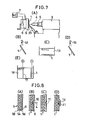
- FIG. 7(A) which represents a modification of the system of FIG. 1(A) and uses the same reference numerals to designate the same parts, elements and materials as previously described, shows a nozzle assembly 23 which directs a flow of the priming solution 9 onto the surface of the dielectric substrate 1 which is locally exposed to the laser beam 4.
- the dielectric substrate 1 can be a composite plate of a glass-fiber woven textile 1A sandwitched between layers 1B of an epoxy resin as shown in FIG. 8. Prior to the simultaneous beam and priming-solution treatment, the substrate 1 is washed with a neutral detergent, water-rinsed and dried.
- the priming solution 9 can be delivered from the nozzle 23 at a flow rate of 50 ml/minute to form a flowing layer on the substrate 1 as shown in FIG. 8(A).
- the beam can be an argon laser beam focused by the lens system 5 to form a beam spot of a diameter of 1 mm at a power density of 1.5 x 10 3 watts/cm 2 on a preselected area of the dielectric surface in contact with the priming solution 9.
- the area irradiated with the energy beam 4 incident through the solution is activated to form.a spot of activation 10 as shown at 10 in FIG. 8(B) and becomes selectively receptive to precipitation of a catalytic nucleus.
- Such nuclei selectively develop along areas swept by the energy beam 4 and remain along those areas as shown at 11 in FIG. 8 after removal of the solution 9 by washing, in the step of FIG. 7 (B), the substrate 1 with chloric acid and then with water followed by drying as previously described.
- the substrate 1 is then introduced into and immersed in the bath of an electroless plating solution 13 as shown in FIG. 7(C) to allow metal 14 therefrom to auto-selectively deposit on the locally primed areas 11 as shown at 14 in FIG. 8(D) and previously described.
- the pattern-plated substrate 1 is rinsed with water from the nozzle 15 as shown in FIG. 7(D).
- the substrate 1 can optionally be introduced into and immersed in the bath of an electrodepositing solution as shown in FIG. 7(E) and previously described to increase the thickness of metal pattern-plated.
- the beam 4 can be swept or displaced to trace the preselected areas at a rate of displacement as high as 220 meters/minute (3.67 m/sec) to allow the precipitation nuclei 11 (FIG. 8(C)) to be sufficiently formed selectively on those areas of the substrate 1.
- a rate of displacement as high as 220 meters/minute (3.67 m/sec) to allow the precipitation nuclei 11 (FIG. 8(C)) to be sufficiently formed selectively on those areas of the substrate 1.
- the energy beam 4 used in the step of FIG. 7(A) is a C0 2 laser beam having a beam diameter of 0.6 cm, a wavelength of 10.6 um and a power of 10 watts.
- the priming solution 9 is an aqueous solution containing 0.1% by weight palladium chloride and 0.3% hydrogen chloride and is caused to flow at a flow rate of 1 cc/sec in a layer of a thickness of 0.1 to 1 mm over the substrate 1.
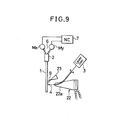
- FIG. 9 shows an arrangement similar to that shown in FIG. 6 using a ultrasonic generator 22 which includes an amplifier horn 22a directed to the dielectric substrate 1 being selectively activated.
- the energy beam 4 from the laser generator 3 is here deflected to pass through an optical guide arranged through the amplifier horn 22a to impinge on selected area of the surface of the substrate 1 in contact with the priming solution 9.
- the substrate 1 lies standing vertically and the nozzle 23 delivers the priming solution flowing down in a thin layer over the substrate 1.
- the ultrasonic generator 22 is activated to apply ultrasonic vibrations or a beam of ultrasonic waves of a frequency of 10 to 50 kHz to the priming solution passing over the localized, laser irradiated area of the substrate 1. With the additional use of the ultrasonic solution activation, it has been found that the rate of catalytic precipitation can be doubled using the same power of the laser beam 4, or that the same rate of catalytic precipitation is achievable using the beam power one fourth lower.
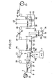
- FIG. 10 shows a continuous system embodying the present invention for continuously processing a dielectric substrate 1 which is in the form of a band dispensed from a supply drum 24 and wound on a takeup drum 25.
- the dielectric band 1 from the supply drum 24 prior to entry into the bath 8 of a priming solution 9 is activation-treated by being exposed to irradiation by a laser beam 4 from the laser generator 3.
- the latter directing the energy beam 4 onto the slowly moving dielectric surface 1 is here securely-mounted on a carriage 2' which is in turn movably carried on a compound drive table 6 provided with a pair of motors Mx, My.
- the motors Mx and My are driven by drive command singles furnished from a numerical control (NC) unit 7 to translationally displace the energy beam in a horizontal plane so that the trajectory of the beam spot on the surface 1 follow a predetermined path programmed in the NC unit 7 to precisely cover preselected areas thereon and to delineate a predetermined pattern to be electrolessly plated with metal.
- NC numerical control
- the dielectric band 1 then passes over a guide roller 26 to enter into the bath 8 of the priming solution 9 to allow the beam-irradiated, preselected areas to be auto-selectively catalyzed upon contact with the solution 9.
- the band 1 passing over a guide roller 27 in the bath 8 is then guided over a cleaning stage defind between a pair of guide rollers 28 and 29 and where it is thoroughly rinsed with water from nozzles 12 removing any residue of the priming solution adherent thereon.
- the band 1 passing over the guide roller 29 is introduced into the bath 13' of an electroless plating solution 13 and moves over guide rollers 30 and 31 therein to allow metal (e.g.
- an electrochemical bath 32 is arranged to communicate with the bath 13' via a pair of conduits 33a and 33b.
- the bath 32 has an anode 34 and a cathode 35 electrically energizable by an external power so that when these electrodes 34 and 35 are energized, the metal is electrolytically dissolved into the solution to replenish the metal therein.
- the band 1 is guided between a pair of further rollers 37 and 38 and in a region therebetween is thoroughly rinsed with water delivered from nozzles 15.
- the band 1 is then guided to enter into the bath 16' of an electroplating solution 16 to pass over guide roller 39, 40 and 41 therein.
- the roller 40 which is electrically conductive is electrically connected to the negative terminal of an electroplating power source 42 and an anode 17 which is positioned adjacent the moving band 1 in the solution 16 is electrically connected to the positive terminal of the power source 42.
- the anode 17 and the cathodic roller are energized by the source 42 to allow the metal from the solution 16 to be electrodeposited on the previously, electrolessly deposited metal (conductive) pattern on the dielectric substrate 1 to increase the metal thickness of the pattern. Passing out of the electroplating bath 16', the band 1 is guided over a further roller 43 and rinsed with water from a nozzle 44 followed by drying prior to winding on the takeup roller 25.
- FIG. 11 shows another continuous system which can be considered as a modification of the system of FIG. 10.
- the band 1 is subjected to irradiation by the energy beam 4 when moving through the bath 8 of the priming solution.
- the dielectric band 1 unwound from the supply drum 24 is passed through the priming solution 9 and over the guide roller 27 to move out of the bath 8.
- the laser generator 3 is securely mounted on the carriage 2' which is here movable horizontally or in an X-Y plane.
- the energy beam 4 from the generator 3 passes through a transparent wall of the walls of a receptacle defining the bath 8' and through the priming solution 9 retained therein and is focused by the lens system 5 to form a narrow beam spot on a selected region of the dielectric substrate 1 in contact with the priming solution.
- the carriage 2' is movable by the compound drive table 6 with the X-axis and Y-axis motors Mx and My.
- These motors are driven by command signals from the NC unit 7 to sweep the laser beam 4 in an vertical plane on the substrate 1 so that the trajectory of the beam spot on the surface 1 follows a predetermined path programmed in the NC unit 7 to precisely cover preselected areas thereon and to allow these areas in contact with the priming solution to be selectively activated and catalized.
- the priming solution 9 can be a palladium-chloride solution composed as tabulated in Table 4 below.
- the priming solution may also be a stannous-chloride solution composed as tabulated in Table 5 below.
- the electroless plating solution 13 can be composed as tabulated in Table 6 below.
- the electroless plating solution 13 can be composed as tabulated in Table 7 below.
- the dielectric surface 1 can, for example, be composed of ABS (acrylonitrile butadiene styrene), polypropylene, epoxy, polyester, phenol, polyphenyl oxide, polyvinyl, urethane or acryl resin, silicon, glass, silica or alumina.
- ABS acrylonitrile butadiene styrene
- polypropylene epoxy
- polyester phenol
- polyphenyl oxide polyvinyl
- urethane or acryl resin silicon, glass, silica or alumina.
Landscapes
- Chemical & Material Sciences (AREA)
- Engineering & Computer Science (AREA)
- Chemical Kinetics & Catalysis (AREA)
- Metallurgy (AREA)
- Materials Engineering (AREA)
- Mechanical Engineering (AREA)
- General Chemical & Material Sciences (AREA)
- Organic Chemistry (AREA)
- Health & Medical Sciences (AREA)
- Toxicology (AREA)
- Physics & Mathematics (AREA)
- Optics & Photonics (AREA)
- Manufacturing & Machinery (AREA)
- Microelectronics & Electronic Packaging (AREA)
- Chemically Coating (AREA)
Applications Claiming Priority (4)
| Application Number | Priority Date | Filing Date | Title |
|---|---|---|---|
| JP6116/84 | 1984-01-17 | ||
| JP611784A JPS60149783A (ja) | 1984-01-17 | 1984-01-17 | 選択的メツキ方法 |
| JP611684A JPS60149782A (ja) | 1984-01-17 | 1984-01-17 | 選択的メツキ方法 |
| JP6117/84 | 1984-01-17 |
Publications (2)
| Publication Number | Publication Date |
|---|---|
| EP0151413A2 true EP0151413A2 (fr) | 1985-08-14 |
| EP0151413A3 EP0151413A3 (fr) | 1985-11-27 |
Family
ID=26340195
Family Applications (1)
| Application Number | Title | Priority Date | Filing Date |
|---|---|---|---|
| EP85100466A Withdrawn EP0151413A3 (fr) | 1984-01-17 | 1985-01-17 | Dépôt métallique sélectif sur une surface diélectrique |
Country Status (2)
| Country | Link |
|---|---|
| US (2) | US4639378A (fr) |
| EP (1) | EP0151413A3 (fr) |
Cited By (7)
| Publication number | Priority date | Publication date | Assignee | Title |
|---|---|---|---|---|
| EP0308011A1 (fr) * | 1987-09-16 | 1989-03-22 | Koninklijke Philips Electronics N.V. | Procédé de dépôt métallique sélectif sur la surface d'un objet |
| EP0489411A1 (fr) * | 1990-12-03 | 1992-06-10 | Xerox Corporation | Méthode pour la catalyse de la métallisation sans courant électrique sur des matières plastiques |
| FR2685559A1 (fr) * | 1991-12-20 | 1993-06-25 | Bosch Gmbh Robert | Dispositif de commande electrique. |
| DE19705745A1 (de) * | 1997-02-14 | 1998-08-20 | Fraunhofer Ges Forschung | Verfahren zum Bilden einer strukturierten Metallisierung auf einem Halbleiterwafer |
| SG102588A1 (en) * | 2000-08-03 | 2004-03-26 | Inst Materials Research & Eng | A process for modifying chip assembly substrates |
| US6863936B2 (en) | 2000-12-19 | 2005-03-08 | Agency For Science, Technology And Research | Method of forming selective electroless plating on polymer surfaces |
| EP1975276A1 (fr) * | 2007-03-30 | 2008-10-01 | Danmarks Tekniske Universitet | Préparation d'un article polymère pour une métallisation sélective |
Families Citing this family (21)
| Publication number | Priority date | Publication date | Assignee | Title |
|---|---|---|---|---|
| US5084299A (en) * | 1989-08-10 | 1992-01-28 | Microelectronics And Computer Technology Corporation | Method for patterning electroless plated metal on a polymer substrate |
| US5192581A (en) * | 1989-08-10 | 1993-03-09 | Microelectronics And Computer Technology Corporation | Protective layer for preventing electroless deposition on a dielectric |
| US5183795A (en) * | 1989-12-13 | 1993-02-02 | Intel Corporation | Fully planar metalization process |
| DE4011114A1 (de) * | 1990-04-06 | 1991-10-10 | Duerrwaechter E Dr Doduco | Verfahren zum bekeimen eines substrats |
| US5171608A (en) * | 1990-09-28 | 1992-12-15 | The Unites States Of America As Represented By The Secretary Of The Navy | Method of pattern transfer in photolithography using laser induced metallization |
| US5382315A (en) * | 1991-02-11 | 1995-01-17 | Microelectronics And Computer Technology Corporation | Method of forming etch mask using particle beam deposition |
| US5244538A (en) * | 1991-07-26 | 1993-09-14 | Microelectronics And Computer Technology Corporation | Method of patterning metal on a substrate using direct-write deposition of a mask |
| US5260108A (en) * | 1992-03-10 | 1993-11-09 | International Business Machines Corporation | Selective seeding of Pd by excimer laser radiation through the liquid |
| US5462773A (en) * | 1992-12-28 | 1995-10-31 | Xerox Corporation | Synchronized process for catalysis of electroless metal plating on plastic |
| BE1008038A5 (fr) * | 1994-01-31 | 1996-01-03 | Lucien Diego Laude | Procede de metallisation de matieres plastiques, et produits ainsi obtenus. |
| EP0694990A1 (fr) * | 1994-07-22 | 1996-01-31 | Connector Systems Technology N.V. | Procédé de métallisation sélective pour connecteurs en plastique |
| FR2761374A1 (fr) * | 1997-03-28 | 1998-10-02 | Gemplus Card Int | Procede de metallisation selective de matieres plastiques intrinseques et carte a circuit(s) integre(s) obtenue selon le procede |
| WO2002092242A1 (fr) * | 2001-05-16 | 2002-11-21 | Board Of Regents | Depot selectif de matieres pour la fabrication d'interconnexions et de contacts sur des dispositifs semi-conducteurs |
| GB2385863A (en) * | 2001-10-29 | 2003-09-03 | Qinetiq Ltd | High resolution patterning method |
| US6899798B2 (en) * | 2001-12-21 | 2005-05-31 | Applied Materials, Inc. | Reusable ceramic-comprising component which includes a scrificial surface layer |
| DE102007010872A1 (de) * | 2007-03-06 | 2008-09-18 | Fraunhofer-Gesellschaft zur Förderung der angewandten Forschung e.V. | Verfahren zur Präzisionsbearbeitung von Substraten und dessen Verwendung |
| US8795788B2 (en) * | 2012-11-14 | 2014-08-05 | Eastman Kodak Company | Method for functional printing system |
| US9072209B2 (en) * | 2012-11-14 | 2015-06-30 | Eastman Kodak Company | Method for forming a conductive pattern |
| US20140366805A1 (en) * | 2012-11-14 | 2014-12-18 | Israel Schuster | System for forming a conductive pattern |
| AU2021329906A1 (en) | 2020-08-18 | 2023-04-27 | Enviro Metals, LLC | Metal refinement |
| CN115160623A (zh) * | 2022-07-11 | 2022-10-11 | 深圳原驰三维技术有限公司 | 一种使聚碳酸酯表面区域选择性吸附金属离子的方法 |
Family Cites Families (9)
| Publication number | Priority date | Publication date | Assignee | Title |
|---|---|---|---|---|
| US2690402A (en) * | 1952-04-01 | 1954-09-28 | Gen Am Transport | Processes of chemical nickel plating of nonmetallic bodies |
| US3364087A (en) * | 1964-04-27 | 1968-01-16 | Varian Associates | Method of using laser to coat or etch substrate |
| US3436468A (en) * | 1965-05-28 | 1969-04-01 | Texas Instruments Inc | Plastic bodies having regions of altered chemical structure and method of making same |
| US3682784A (en) * | 1970-04-21 | 1972-08-08 | Rca Corp | Process for forming a conductive coating on a substrate |
| US3839083A (en) * | 1972-10-06 | 1974-10-01 | Texas Instruments Inc | Selective metallization process |
| US3954570A (en) * | 1974-11-11 | 1976-05-04 | Amp Incorporated | Sensitized polyimides and circuit elements thereof |
| CH610596A5 (fr) * | 1977-02-16 | 1979-04-30 | Ebauches Sa | |
| DE3138474A1 (de) * | 1981-09-26 | 1983-04-14 | Licentia Patent-Verwaltungs-Gmbh, 6000 Frankfurt | "verfahren zur selektiven chemischen metallisierung" |
| US4440801A (en) * | 1982-07-09 | 1984-04-03 | International Business Machines Corporation | Method for depositing a metal layer on polyesters |
-
1985
- 1985-01-16 US US06/691,877 patent/US4639378A/en not_active Expired - Fee Related
- 1985-01-17 EP EP85100466A patent/EP0151413A3/fr not_active Withdrawn
-
1986
- 1986-07-07 US US06/882,498 patent/US4822633A/en not_active Expired - Fee Related
Cited By (12)
| Publication number | Priority date | Publication date | Assignee | Title |
|---|---|---|---|---|
| EP0308011A1 (fr) * | 1987-09-16 | 1989-03-22 | Koninklijke Philips Electronics N.V. | Procédé de dépôt métallique sélectif sur la surface d'un objet |
| EP0489411A1 (fr) * | 1990-12-03 | 1992-06-10 | Xerox Corporation | Méthode pour la catalyse de la métallisation sans courant électrique sur des matières plastiques |
| FR2685559A1 (fr) * | 1991-12-20 | 1993-06-25 | Bosch Gmbh Robert | Dispositif de commande electrique. |
| US5285010A (en) * | 1991-12-20 | 1994-02-08 | Robert Bosch Gmbh | Electrical control device with metal-coated plastic housing |
| DE19705745A1 (de) * | 1997-02-14 | 1998-08-20 | Fraunhofer Ges Forschung | Verfahren zum Bilden einer strukturierten Metallisierung auf einem Halbleiterwafer |
| US6284639B1 (en) | 1997-02-14 | 2001-09-04 | Fraunhofer-Gesellschaft Zur Foerderung Der Angwandten Forschung E.V. | Method for forming a structured metallization on a semiconductor wafer |
| DE19705745C2 (de) * | 1997-02-14 | 2002-02-07 | Fraunhofer Ges Forschung | Verfahren zum Bilden einer strukturierten Metallisierung auf einem Halbleiterwafer |
| SG102588A1 (en) * | 2000-08-03 | 2004-03-26 | Inst Materials Research & Eng | A process for modifying chip assembly substrates |
| US6863936B2 (en) | 2000-12-19 | 2005-03-08 | Agency For Science, Technology And Research | Method of forming selective electroless plating on polymer surfaces |
| EP1975276A1 (fr) * | 2007-03-30 | 2008-10-01 | Danmarks Tekniske Universitet | Préparation d'un article polymère pour une métallisation sélective |
| WO2008119359A1 (fr) * | 2007-03-30 | 2008-10-09 | Danmarks Tekniske Universitet | Préparation d'un article polymère destiné à une métallisation sélective |
| US8628831B2 (en) | 2007-03-30 | 2014-01-14 | Danmarks Tekniskie Universitet | Preparation of a polymer article for selective metallization |
Also Published As
| Publication number | Publication date |
|---|---|
| US4822633A (en) | 1989-04-18 |
| EP0151413A3 (fr) | 1985-11-27 |
| US4639378A (en) | 1987-01-27 |
Similar Documents
| Publication | Publication Date | Title |
|---|---|---|
| US4639378A (en) | Auto-selective metal deposition on dielectric surfaces | |
| EP0128401B1 (fr) | Procédé chimique d'addition ou de soustraction | |
| US8529738B2 (en) | In situ plating and etching of materials covered with a surface film | |
| US20110042201A1 (en) | In situ Plating And Soldering Of Materials Covered With A Surface Film | |
| EP0489411B1 (fr) | Méthode pour la catalyse de la métallisation sans courant électrique sur des matières plastiques | |
| US4349583A (en) | Laser enhanced maskless method for plating and simultaneous plating and etching of patterns | |
| JP3153682B2 (ja) | 回路板の製造方法 | |
| EP0150358B1 (fr) | Décapage chimique de métaux induit par laser | |
| US4981715A (en) | Method of patterning electroless plated metal on a polymer substrate | |
| US5182230A (en) | Laser methods for circuit repair on integrated circuits and substrates | |
| WO2002103771A1 (fr) | Dispositif de traitement electrolytique et appareil de traitement de substrat | |
| Niino et al. | Positively charged surface potential of polymer films after excimer laser ablation: application to selective‐area electroless plating on the ablated films | |
| EP0231795B1 (fr) | Procédé de fabrication de circuits imprimés | |
| JPH07180089A (ja) | 電気鍍金方法及び構成 | |
| EP0131367A1 (fr) | Procédé et appareil pour l'usinage de matières en céramique | |
| US6972082B2 (en) | Method for the selectively electroplating a strip-shaped, metal support material | |
| US20020102745A1 (en) | Process for modifying chip assembly substrates | |
| Pimenov et al. | Laser activation of diamond surface for electroless metal plating | |
| JP3305425B2 (ja) | プラズマ加工方法 | |
| KR20020031178A (ko) | 유전 기층 상의 전도성 패턴의 제조 방법 | |
| US6106690A (en) | Electroplaner | |
| JPH0577748B2 (fr) | ||
| KR960014699B1 (ko) | 연속 드라이 프로세스 코팅방법 및 그 장치 | |
| US6960282B2 (en) | Apparatus for cleaning residual material from an article | |
| JPH0534428B2 (fr) |
Legal Events
| Date | Code | Title | Description |
|---|---|---|---|
| PUAI | Public reference made under article 153(3) epc to a published international application that has entered the european phase |
Free format text: ORIGINAL CODE: 0009012 |
|
| AK | Designated contracting states |
Designated state(s): CH DE FR GB LI |
|
| PUAL | Search report despatched |
Free format text: ORIGINAL CODE: 0009013 |
|
| AK | Designated contracting states |
Designated state(s): CH DE FR GB LI |
|
| 17P | Request for examination filed |
Effective date: 19851219 |
|
| 17Q | First examination report despatched |
Effective date: 19861201 |
|
| STAA | Information on the status of an ep patent application or granted ep patent |
Free format text: STATUS: THE APPLICATION HAS BEEN WITHDRAWN |
|
| 18W | Application withdrawn |
Withdrawal date: 19900305 |
|
| APAF | Appeal reference modified |
Free format text: ORIGINAL CODE: EPIDOSCREFNE |
|
| RIN1 | Information on inventor provided before grant (corrected) |
Inventor name: INOUE, KIYOSHI |