EP0151829A1 - Interpolierender Filter mit irrationalem Verhältnis zwischen den Eingangs- und Ausgangsabtastfrequenzen - Google Patents
Interpolierender Filter mit irrationalem Verhältnis zwischen den Eingangs- und Ausgangsabtastfrequenzen Download PDFInfo
- Publication number
- EP0151829A1 EP0151829A1 EP84201914A EP84201914A EP0151829A1 EP 0151829 A1 EP0151829 A1 EP 0151829A1 EP 84201914 A EP84201914 A EP 84201914A EP 84201914 A EP84201914 A EP 84201914A EP 0151829 A1 EP0151829 A1 EP 0151829A1
- Authority
- EP
- European Patent Office
- Prior art keywords
- input
- filter
- output
- signal
- samples
- Prior art date
- Legal status (The legal status is an assumption and is not a legal conclusion. Google has not performed a legal analysis and makes no representation as to the accuracy of the status listed.)
- Granted
Links
Images


Classifications
-
- H—ELECTRICITY
- H03—ELECTRONIC CIRCUITRY
- H03H—IMPEDANCE NETWORKS, e.g. RESONANT CIRCUITS; RESONATORS
- H03H17/00—Networks using digital techniques
-
- H—ELECTRICITY
- H03—ELECTRONIC CIRCUITRY
- H03H—IMPEDANCE NETWORKS, e.g. RESONANT CIRCUITS; RESONATORS
- H03H17/00—Networks using digital techniques
- H03H17/02—Frequency selective networks
- H03H17/06—Non-recursive filters
- H03H17/0621—Non-recursive filters with input-sampling frequency and output-delivery frequency which differ, e.g. extrapolation; Anti-aliasing
- H03H17/0635—Non-recursive filters with input-sampling frequency and output-delivery frequency which differ, e.g. extrapolation; Anti-aliasing characterized by the ratio between the input-sampling and output-delivery frequencies
- H03H17/0642—Non-recursive filters with input-sampling frequency and output-delivery frequency which differ, e.g. extrapolation; Anti-aliasing characterized by the ratio between the input-sampling and output-delivery frequencies the ratio being arbitrary or irrational
Definitions
- the invention relates to an interpolating time-discrete filter arrangement for converting a time-discrete input signal with which an input sampling frequency f i is associated into a time-discrete output signal with which an output sampling frequency f is associated which is higher than the input sampling frequency.
- A(2) Description of the prior art.
- a time-discrete signal is formed by a series of signal samples.
- the sampling frequency associated with such a signal indicates the rate at which these signal samples occur.
- the signal sample itself indicates the magnitude of the signal at a given instant. Within a certain range such a signal sample can assume any value, or only one of a number of discrete values. In the latter case a digital signal is involved and the signal sample is usually represented by a code word having a plurality of bits.
- interpolating filters are extensively described in, for example, the References 3, 4 and 5. Like all types of time-discrete filter arrangements they comprise a signal processing circuit to which the time-discrete input signal and also filter coefficients are applied. As is known, these filter coefficients represent samples of the finite impulse response of the filter and are produced by a filter coefficients generator.
- the invention has for its object to provide an interpolating filter arrangement having an irrational interpolation factor.
- this filter arrangement is therefore provided with :
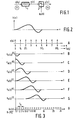
- Fig. 1 shows schematically the theoretical model of a time-discrete filter arrangement for changing the sampling frequency of a time-discrete input signal. It comprises an "analog" filter 1 followed by a sampling arrangement 2.
- This filter supplies an output signal z(t) which is equal to the sum of all the so-called individual output signals z x(q) (t).
- the response of this filter 1 to the input sample x(q) produces such an individual output signal.
- this individual output signal is thus equal to the product of this input sample and the impulse response of this filter. If this impulse response is represented by the function h(v), this individual output signal can be expressed mathematically as follows :
- the actual output signal z(t) of this filter 1 is formed by the mathematical sum of all the individual output signals. Since the impulse response is finite, the number of individual output signals contributing to the ultimate output signal z(t) is also finite. Let it be assumed that of only M individual output signals this contribution is unequal to zero, that the filter is a causal filter and that the input signal sample applied last to the filter has the number g, then it holds that :
- the sampling arrangement 2 produces a series of output samples, the output sample obtained in response to the n th sampling pulse ku(n) being denoted by y(n) and being defined by the expression:
- the quantities h(T d(q-m) +wT u ) wherein w (n q -n q-m +r), represent the filter coefficients of the time-discrete filter arrangement. In the following paragraph these filter coefficients will be denoted for the sake of brevity by a(d(q),w).
- the quantity d(q) will be called the deviation component and is defined as follows :
- the interpolation factor may have any random positive value exceeding or equal to unity. In this paragraph some special cases will be further described.
- a decimating time-discrete filter arrangement having a decimation factor P can be arranged in cascade with an interpolating time-discrete filter arrangement having an interpolation factor L.
- Interpolating time-discrete filter arrangements of this type are described in, for example, References 3, 5 and 6.
- Fig. 4 shows schematically an embodiment of an interpolating time-discrete filter arrangement having an irrational interpolation factor.
- it comprises a signal processing arrangement 3 and a filter coefficients generator 4.
- This signal processing arrangement 3 is preceded by a buffer store 5 to which the input samples x(q) are applied.
- Such an input sample x(q) is stored in this buffer store at the instant at which an input clock pulse ki(q) occurs at its write input WR.
- an output clock pulse ku(n) is applied to the read input R of this buffer store, the content of this buffer store is applied to the signal processing arrangement 3. Let it now be assumed that this buffer store is reset as a result thereof.
- this buffer store supplies a signal sample having the value zero.
- the input clock pulses ki(q) are produced by a clock pulse generator 6 and occur with the input sampling frequency f..
- the output clock pulses ku(n) are produced by a clock pulse generator 7 and occur with the output sampling frequency f u .
- this deviation component represents the ratio between the time interval T d(q) located between the input sample x(q) and the immediately subsequent output sample y(n q ) and the output sampling period T u or, which is the same, the ratio between the time interval located between the instant t ki(q) at which an input clock pulse ki(q) occurs and the instant t ku(nq) at which an immediately subsequent output clock pulse ku(n ) occurs and the interval T u between two conse- cutive output pulses.
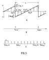
- the generator comprises a, preferably digital, sawtooth generator 400 which produces at a rate f u digitally encoded samples of a periodic analog sawtooth-shaped signal which has a period ..
- the generator 400 may be assumed to comprise a sawtooth generator 400(1) which is controlled by the input clock pulses ki(q). This generator produces, for example, the analog sawtooth-shaped signal shown at A in Fig.
- the deviation component d(q) can be fully determined from the value of the signal samples of the sawtooth signal.
- these signal samples s(n) are applied for this purpose to a cascade arrangement of two shift register elements 401 and 402 and to a shift register element 403. The contents of these shift register elements are shifted under the control of the output clock pulses ku(n).
- the signal samples s(n) are also applied to a zero-crossing detector circuit 404 which produces a detection pulse each time a signal sample of the positive polarity is followed by a signal sample of the negative polarity. This detection pulse is applied to the clock pulse inputs of two further shift register elements 405 and 406.
- the signal inputs thereof are connected to the signal outputs of the respective shift register elements 402 and 403.
- the contents of the shift register elements 405 and 406 become equal to s(n q -1) and s(n q ), respectively.
- subtracting arrangements 407 and 408 the absolute value of these signal samples is subtracted from the value E.
- the two difference components thus obtained are added together in an adder arrangement 409 and the sum component O(n q ) thus obtained is divided in a divider stage 410 by the difference component produced by subtracting arrangement 407.
- the deviation component d(q) thus obtained is applied to an arithmetic unit 411 (for example a microcomputer) which is arranged to calculate at the given value of d(q) the required filter coefficients a(d(q),w) (four in the case described) in accordance with expression (14).
- an arithmetic unit 411 for example a microcomputer
- arithmetic unit 411 for example a microcomputer
- the factor 1-d(q) can be obtained by dividing the output signal of the subtracting arrangement 408 (see Fig. 4) by the sum component O(n q ).
- the output signal of the subtracting arrangement 408 is applied to a divider stage 412, which also receives the sum component 0(nq) from adder arrangement 409.
- the output components of the two divider stages 410 and 412 are multiplied by the constant H in multiplier stages 413 and 414.
- the signal processing arrangement 3 now supplies output samples y'(n) which are applied to a multiplying circuit in which they are multiplied by H/O(n q ), as a result of which the desired output samples y(n) can be obtained.
- the signal samples s(n) are obtained by sampling an analog sawtooth signal.
- a sawtooth generator which produces these signal samples in a fully digital way is shown in Fig. 8.
- the generator comprises an input circuit which includes a D flip-flop 414. The D-input thereof continuously receives the logic value "1".
- the clock input CL receives the input clock pulses ki(q) and the reset input R receives a reset signal.
- the Q-output of this D-flip-flop 414 is connected to the D-input of a D-flip-flop 415.
- the output clock pulses ku(n) are applied to the clock pulse input CL of this flip-flop.
- the pulses occurring at the Q-output of the D-flip-flop 415 and the output clock pulses ku(n) inverted in an inverter 416 are applied to a NAND-gate 417 the output pulses of which are applied as reset pulses to the reset input R of D-flip-flop 414.
- This input circuit formed by two D-flip-flops may, for example, be the dual D-flip-flop of the "74" series marketed by Signetics.
- the output pulses of D-flip-flop 415 are applied to a phase- locked loop (PLL) which is of a digital construction.
- PLL phase- locked loop
- This loop comprises an up/down counter 418 whose counting range is located in the range 0-2E.
- the output pulses of D-flip-flop 415 are applied to its up-counting input (+).
- the counting position of this counter 418 is applied with intervals T u to a digital low-pass filter 420 via a sub- tracting arrangement 419.
- the subtracting arrangement 419 the counting position is reduced by a reference number REF which is, for example, equal to half(E) of the range (2E) of counter 418.
- the low-pass filter 420 which has a bandwidth of less than 1 Hz, produces at a rate f u output numbers which are applied to an accumulator formed by an adder 421 and a delay network 422 whose time delay is equal to T .
- Adder 421 has two outputs denoted by c and e, respectively. At the output c the (most significant) carry bit occurs of the word produced by the adder, whilst the remaining bits of this word occur at the output e.
- the output c is further connected to the down-counting input (-) of the up/down counter 418 and the output e represents at the same time the output of the sawtooth generator.
- generator 400(1) produces a sawtooth signal. It is, however, alternatively possible to construct this generator such that it produces a signal which varies triangularly in the way shown in, for example, Fig. 9.
- the two signal samples s(n +2) and s(q +3) may be the starting point. It should be noted that this is also possible for the case shown schematically in Fig. 5 where a sawtooth-shaped signal is involved. In that case the zero-crossing detector 404 must produce an output pulse for each signal sample having a negative polarity followed by a signal sample having a positive polarity.
- the filter coefficients generator 4 operates as follows.
- the time interval T between two consecutive out- u put clock pulses ku(n) is distributed in an infinite number of sub-intervals T uo which are infinitely small. Thereafter it is determined between which two consecutive output clock pulses ku(n) the input clock pulse ki(q) is located and also in which sub-interval.
- the number of this sub-interval may be considered to be the deviation component d(q).
- the number of sub-intervals now depends on the number of bits by which d(q) is represented. If this number of bits is chosen such that a countable number of sub-intervals is obtained, the following procedure can be followed.
- the MR' filter coefficients a(d(q),w) associated with each value of the deviation component can be calculated in advance and stored in a storage medium. Let it be assumed that the deviation component can assume sixteen different values, then this storage medium contains, for example, 16 MR' filter coefficients. A selector to which the deviation component is applied and which depending on the value thereof selects the desired group from these sixteen groups of filter coefficients. In such cases the term "table look up" is sometimes used.
- a particularly suitable embodiment of the signal processing arrangement is known from Fig. 9.10 of Reference 7 and is shown in Fig. 10, for the sake of completeness. It comprises in known manner a number of MR' multiplying circuits 30(.) (4 in the embodiment shown), a plurality of adder circuits 31(.) and a plurality of delay circuits 32(.), each having a time delay T . All the multiplying circuits are connected by means of an input to the input 33 of the signal processing arrangement and thus receive the input samples x(q) simultaneously. In addition they receive via a filter coefficients inputs the required filter coefficients produced by the filter coefficients generator shown in Fig. 4. The desired output samples now occur at the output 35 of adder circuit 31(2).
- FIG. 11 An alternative embodiment of the signal processing arrangement 3 is shown for the greater part in Fig. 9.1 of Reference 7 and, for the sake of completeness, is shown in Fig. 11. It comprises a cascade arrangement of a number of delay devices 36(.) (three in the embodiment shown), each having a time delay T . This cascade arrangement is connected to the input 33 of the signal processing arrangement. Inputs and outputs of the delay devices 36(.) are connected via multiplying circuits 30(.) to inputs of an adder device 37, which supplies the desired output samples y(n) from its output 35. The multiplying circuits 30(.) receive the required filter coefficients via their filter coefficients inputs.
- the filter coefficients a(d(q),0) are directly applied to the multiplying circuit 30(0), and the filter coefficients a(d(q),l) are applied to the multiplying circuit 30(1) via a delay device 38(1) having a time delay T u .
- the filter coefficients a(d(q),2) and a(d(q),3) are applied to the respective multiplying circuits 30(2) and 30(3) via delay devices 38(2) and 38(3) having the respective time delays 2Tu and 3T u .
- calculating the deviation component d(q) was based on the time interval located between an input clock pulse ki(q) and the immediately preceding output clock pulse ku(n). It is, however, also permissible to define this deviation component as the quotient between the time interval located between an input clock pulse ki(q) and the immediately preceding output clock pulse ku(n-1) and the time interval T between two consecutive output clock pulses.
Landscapes
- Physics & Mathematics (AREA)
- Engineering & Computer Science (AREA)
- Computer Hardware Design (AREA)
- Mathematical Physics (AREA)
- Complex Calculations (AREA)
- Transmission Systems Not Characterized By The Medium Used For Transmission (AREA)
- Analogue/Digital Conversion (AREA)
- Television Systems (AREA)
- Filters That Use Time-Delay Elements (AREA)
- Facsimile Image Signal Circuits (AREA)
- Filters And Equalizers (AREA)
Priority Applications (1)
| Application Number | Priority Date | Filing Date | Title |
|---|---|---|---|
| AT84201914T ATE41576T1 (de) | 1984-01-10 | 1984-12-19 | Interpolierender filter mit irrationalem verhaeltnis zwischen den eingangs- und ausgangsabtastfrequenzen. |
Applications Claiming Priority (2)
| Application Number | Priority Date | Filing Date | Title |
|---|---|---|---|
| NL8400073A NL8400073A (nl) | 1984-01-10 | 1984-01-10 | Interpolerende filterinrichting met niet-rationale verhouding tussen de ingangs- en uitgangsbemonsterfrequentie. |
| NL8400073 | 1984-01-10 |
Publications (2)
| Publication Number | Publication Date |
|---|---|
| EP0151829A1 true EP0151829A1 (de) | 1985-08-21 |
| EP0151829B1 EP0151829B1 (de) | 1989-03-15 |
Family
ID=19843301
Family Applications (1)
| Application Number | Title | Priority Date | Filing Date |
|---|---|---|---|
| EP84201914A Expired EP0151829B1 (de) | 1984-01-10 | 1984-12-19 | Interpolierender Filter mit irrationalem Verhältnis zwischen den Eingangs- und Ausgangsabtastfrequenzen |
Country Status (12)
| Country | Link |
|---|---|
| US (1) | US4604720A (de) |
| EP (1) | EP0151829B1 (de) |
| JP (1) | JPH0642619B2 (de) |
| KR (1) | KR930001296B1 (de) |
| AT (1) | ATE41576T1 (de) |
| AU (1) | AU584597B2 (de) |
| CA (1) | CA1241381A (de) |
| DE (1) | DE3477327D1 (de) |
| ES (1) | ES8606751A1 (de) |
| HK (1) | HK86191A (de) |
| NL (1) | NL8400073A (de) |
| SG (1) | SG85390G (de) |
Cited By (3)
| Publication number | Priority date | Publication date | Assignee | Title |
|---|---|---|---|---|
| EP0227172A1 (de) * | 1985-12-18 | 1987-07-01 | Koninklijke Philips Electronics N.V. | Phasenregelschleife für Filteranordnung mit nicht-rationellem Verhältnis zwischen Ein- und Ausgangsabtastfrequenz |
| JPH027710A (ja) * | 1988-02-04 | 1990-01-11 | American Teleph & Telegr Co <Att> | 横フィルタ |
| EP0665546A3 (de) * | 1994-01-26 | 1996-04-03 | Sony Corp | Abtastfrequenzumsetzeinrichtung und Steuereinrichtung für Speicheradresse. |
Families Citing this family (38)
| Publication number | Priority date | Publication date | Assignee | Title |
|---|---|---|---|---|
| DE3171426D1 (en) * | 1980-11-26 | 1985-08-22 | Studer Willi Ag | Method and circuit for converting the sampling frequency of a series of samples avoiding conversion into a continuous signal |
| FR2548851B1 (fr) * | 1983-07-07 | 1986-11-14 | Electricite De France | Procede et installation d'analyse et de restitution de signal a echantillonnage et interpolation |
| US4761752A (en) * | 1986-04-21 | 1988-08-02 | North American Philips Corporation | Fractional step correlator |
| US4700226A (en) * | 1986-10-17 | 1987-10-13 | Rca Corporation | Rate buffer control of predicted signal decimation and interpolation for adaptive differential pulse code modulator |
| US5473555A (en) * | 1988-08-18 | 1995-12-05 | Hewlett-Packard Company | Method and apparatus for enhancing frequency domain analysis |
| US5235534A (en) * | 1988-08-18 | 1993-08-10 | Hewlett-Packard Company | Method and apparatus for interpolating between data samples |
| EP0356597B1 (de) * | 1988-08-30 | 1994-03-30 | International Business Machines Corporation | Massnahmen zur Verbesserung des Verfahrens und Vorrichtung eines digitalen Frequenzumsetzungsfilters |
| ATE150073T1 (de) | 1988-12-05 | 1997-03-15 | Unilever Nv | Wässrige schmiermittellösungen auf der basis von fettalkylaminen |
| JPH10294646A (ja) * | 1990-02-16 | 1998-11-04 | Sony Corp | サンプリングレート変換装置 |
| US5475628A (en) * | 1992-09-30 | 1995-12-12 | Analog Devices, Inc. | Asynchronous digital sample rate converter |
| US5440593A (en) * | 1993-09-30 | 1995-08-08 | Ati Technologies Inc. | Combined aligner blender |
| EP0657999B1 (de) * | 1993-12-08 | 2000-05-31 | Nokia Mobile Phones Ltd. | Verfahren zur Umsetzung der Abtastfrequenz |
| EP0695032B1 (de) * | 1994-07-25 | 2001-11-07 | Matsushita Electric Industrial Co., Ltd. | Digital/Digital-Abtastratenumsetzer |
| US5638010A (en) * | 1995-06-07 | 1997-06-10 | Analog Devices, Inc. | Digitally controlled oscillator for a phase-locked loop providing a residue signal for use in continuously variable interpolation and decimation filters |
| US5903480A (en) * | 1997-09-29 | 1999-05-11 | Neomagic | Division-free phase-shift for digital-audio special effects |
| US7228109B2 (en) * | 2001-01-12 | 2007-06-05 | Silicon Laboratories Inc. | DC offset reduction in radio-frequency apparatus and associated methods |
| US6993314B2 (en) | 1998-05-29 | 2006-01-31 | Silicon Laboratories Inc. | Apparatus for generating multiple radio frequencies in communication circuitry and associated methods |
| US6804497B2 (en) * | 2001-01-12 | 2004-10-12 | Silicon Laboratories, Inc. | Partitioned radio-frequency apparatus and associated methods |
| US7221921B2 (en) * | 1998-05-29 | 2007-05-22 | Silicon Laboratories | Partitioning of radio-frequency apparatus |
| US7035607B2 (en) * | 1998-05-29 | 2006-04-25 | Silicon Laboratories Inc. | Systems and methods for providing an adjustable reference signal to RF circuitry |
| US7092675B2 (en) * | 1998-05-29 | 2006-08-15 | Silicon Laboratories | Apparatus and methods for generating radio frequencies in communication circuitry using multiple control signals |
| US7024221B2 (en) * | 2001-01-12 | 2006-04-04 | Silicon Laboratories Inc. | Notch filter for DC offset reduction in radio-frequency apparatus and associated methods |
| US7242912B2 (en) * | 1998-05-29 | 2007-07-10 | Silicon Laboratories Inc. | Partitioning of radio-frequency apparatus |
| US6970717B2 (en) | 2001-01-12 | 2005-11-29 | Silicon Laboratories Inc. | Digital architecture for radio-frequency apparatus and associated methods |
| US5900392A (en) * | 1998-07-24 | 1999-05-04 | Loeffler Chemical Corporation | Aqueous belt lubricant composition based on fatty alkyl propylene tettramines and fatty alcohol polyglycol ethers and method for lubricating belt conveyor systems |
| US6903617B2 (en) | 2000-05-25 | 2005-06-07 | Silicon Laboratories Inc. | Method and apparatus for synthesizing high-frequency signals for wireless communications |
| US20030232613A1 (en) * | 2001-01-12 | 2003-12-18 | Kerth Donald A. | Quadrature signal generation in radio-frequency apparatus and associated methods |
| US7035611B2 (en) * | 2001-01-12 | 2006-04-25 | Silicon Laboratories Inc. | Apparatus and method for front-end circuitry in radio-frequency apparatus |
| US7031683B2 (en) * | 2001-01-12 | 2006-04-18 | Silicon Laboratories Inc. | Apparatus and methods for calibrating signal-processing circuitry |
| US7138858B2 (en) | 2001-01-12 | 2006-11-21 | Silicon Laboratories, Inc. | Apparatus and methods for output buffer circuitry with constant output power in radio-frequency circuitry |
| US7158574B2 (en) * | 2001-01-12 | 2007-01-02 | Silicon Laboratories Inc. | Digital interface in radio-frequency apparatus and associated methods |
| US7177610B2 (en) * | 2001-01-12 | 2007-02-13 | Silicon Laboratories Inc. | Calibrated low-noise current and voltage references and associated methods |
| US8467483B2 (en) * | 2002-03-15 | 2013-06-18 | Silicon Laboratories Inc. | Radio-frequency apparatus and associated methods |
| US8855254B2 (en) * | 2010-03-05 | 2014-10-07 | The Aerospace Corporation | Systems and methods for pre-averaged staggered convolution decimating filters |
| US8489662B2 (en) * | 2010-03-05 | 2013-07-16 | The Aerospace Corporation | Systems and methods for sliding convolution interpolating filters |
| US9797961B2 (en) * | 2015-01-19 | 2017-10-24 | Allegro Microsystems, Llc | Magnetic field sensor with delayed output |
| DE102016110540B4 (de) | 2016-06-08 | 2022-01-20 | Krones Aktiengesellschaft | Vorrichtung und Verfahren zum Inspizieren von Behältnissen |
| US10866288B2 (en) | 2019-05-14 | 2020-12-15 | Allegro Microsystems, Llc | Digital interpolation of switch point to reduce switch point jitter |
Citations (3)
| Publication number | Priority date | Publication date | Assignee | Title |
|---|---|---|---|---|
| EP0052847A2 (de) * | 1980-11-26 | 1982-06-02 | WILLI STUDER AG Fabrik für elektronische Apparate | Verfahren und Schaltungsanordnung zur Umsetzung der Abtastfrequenz einer Abtastfolge unter Umgehung der Konversion in ein kontinuierliches Signal |
| EP0099600A1 (de) * | 1982-07-05 | 1984-02-01 | Koninklijke Philips Electronics N.V. | Filteranordnung mit Herabsetzung der Abtastfrequenz |
| EP0137323A2 (de) * | 1983-10-06 | 1985-04-17 | Studer Revox Ag | Verfahren und Vorrichtung zur Umsetzung einer Eingangsabtastfolge in eine Ausgangsabtastfolge |
Family Cites Families (7)
| Publication number | Priority date | Publication date | Assignee | Title |
|---|---|---|---|---|
| US3829670A (en) * | 1972-04-10 | 1974-08-13 | Massachusetts Inst Technology | Digital filter to realize efficiently the filtering required when multiplying or dividing the sampling rate of a digital signal by a composite integer |
| NL168669C (nl) * | 1974-09-16 | 1982-04-16 | Philips Nv | Interpolerend digitaal filter met ingangsbuffer. |
| US4020332A (en) * | 1975-09-24 | 1977-04-26 | Bell Telephone Laboratories, Incorporated | Interpolation-decimation circuit for increasing or decreasing digital sampling frequency |
| NL7905577A (nl) * | 1979-07-18 | 1981-01-20 | Philips Nv | Inrichting met een niet-recursieffilter. |
| US4270026A (en) * | 1979-11-28 | 1981-05-26 | International Telephone And Telegraph Corporation | Interpolator apparatus for increasing the word rate of a digital signal of the type employed in digital telephone systems |
| US4460890A (en) * | 1982-01-21 | 1984-07-17 | Sony Corporation | Direct digital to digital sampling rate conversion, method and apparatus |
| WO1991016431A1 (en) * | 1990-04-24 | 1991-10-31 | Schering Corporation | Soluble, truncated gamma-interferon receptors |
-
1984
- 1984-01-10 NL NL8400073A patent/NL8400073A/nl not_active Application Discontinuation
- 1984-03-16 US US06/590,096 patent/US4604720A/en not_active Expired - Fee Related
- 1984-12-19 AT AT84201914T patent/ATE41576T1/de not_active IP Right Cessation
- 1984-12-19 EP EP84201914A patent/EP0151829B1/de not_active Expired
- 1984-12-19 DE DE8484201914T patent/DE3477327D1/de not_active Expired
-
1985
- 1985-01-03 CA CA000471446A patent/CA1241381A/en not_active Expired
- 1985-01-07 ES ES539384A patent/ES8606751A1/es not_active Expired
- 1985-01-08 JP JP60000486A patent/JPH0642619B2/ja not_active Expired - Lifetime
- 1985-01-08 KR KR1019850000052A patent/KR930001296B1/ko not_active Expired - Fee Related
- 1985-01-08 AU AU37384/85A patent/AU584597B2/en not_active Ceased
-
1990
- 1990-10-24 SG SG853/90A patent/SG85390G/en unknown
-
1991
- 1991-10-31 HK HK861/91A patent/HK86191A/en unknown
Patent Citations (3)
| Publication number | Priority date | Publication date | Assignee | Title |
|---|---|---|---|---|
| EP0052847A2 (de) * | 1980-11-26 | 1982-06-02 | WILLI STUDER AG Fabrik für elektronische Apparate | Verfahren und Schaltungsanordnung zur Umsetzung der Abtastfrequenz einer Abtastfolge unter Umgehung der Konversion in ein kontinuierliches Signal |
| EP0099600A1 (de) * | 1982-07-05 | 1984-02-01 | Koninklijke Philips Electronics N.V. | Filteranordnung mit Herabsetzung der Abtastfrequenz |
| EP0137323A2 (de) * | 1983-10-06 | 1985-04-17 | Studer Revox Ag | Verfahren und Vorrichtung zur Umsetzung einer Eingangsabtastfolge in eine Ausgangsabtastfolge |
Non-Patent Citations (1)
| Title |
|---|
| PROCEEDINGS OF THE IEEE, vol. 61, no. 6, June 1973, pages 692-702, New York, US; R.W. SCHAFER et al.: "A digital signal processing approach to interpolation" * |
Cited By (6)
| Publication number | Priority date | Publication date | Assignee | Title |
|---|---|---|---|---|
| EP0227172A1 (de) * | 1985-12-18 | 1987-07-01 | Koninklijke Philips Electronics N.V. | Phasenregelschleife für Filteranordnung mit nicht-rationellem Verhältnis zwischen Ein- und Ausgangsabtastfrequenz |
| JPH027710A (ja) * | 1988-02-04 | 1990-01-11 | American Teleph & Telegr Co <Att> | 横フィルタ |
| EP0327268A3 (de) * | 1988-02-04 | 1992-08-05 | AT&T Corp. | Interpolator und Verfahren zur Interpolierung von digitalen Signalmustern |
| EP0665546A3 (de) * | 1994-01-26 | 1996-04-03 | Sony Corp | Abtastfrequenzumsetzeinrichtung und Steuereinrichtung für Speicheradresse. |
| US5617088A (en) * | 1994-01-26 | 1997-04-01 | Sony Corporation | Sampling frequency converting device and memory address control device |
| US5835032A (en) * | 1994-01-26 | 1998-11-10 | Sony Corporation | Sampling frequency converting device and memory address control device |
Also Published As
| Publication number | Publication date |
|---|---|
| US4604720A (en) | 1986-08-05 |
| KR850005747A (ko) | 1985-08-28 |
| CA1241381A (en) | 1988-08-30 |
| KR930001296B1 (ko) | 1993-02-25 |
| ATE41576T1 (de) | 1989-04-15 |
| ES539384A0 (es) | 1986-04-01 |
| SG85390G (en) | 1991-01-04 |
| HK86191A (en) | 1991-11-08 |
| DE3477327D1 (en) | 1989-04-20 |
| ES8606751A1 (es) | 1986-04-01 |
| JPH0642619B2 (ja) | 1994-06-01 |
| AU584597B2 (en) | 1989-06-01 |
| EP0151829B1 (de) | 1989-03-15 |
| NL8400073A (nl) | 1985-08-01 |
| AU3738485A (en) | 1985-07-18 |
| JPS60217714A (ja) | 1985-10-31 |
Similar Documents
| Publication | Publication Date | Title |
|---|---|---|
| US4604720A (en) | Interpolating filter arrangement with non-rational ratio between the input and the output sampling frequencies | |
| US4584659A (en) | Decimation filter arrangement | |
| EP0084945B1 (de) | Verfahren und Anordnung zur direkt digitalen/digitalen Abtastratenumsetzung | |
| EP0227172B1 (de) | Phasenregelschleife für Filteranordnung mit nicht-rationellem Verhältnis zwischen Ein- und Ausgangsabtastfrequenz | |
| US3997773A (en) | Interpolating digital filter with input buffer | |
| JP2986745B2 (ja) | 複合位相濾波器とこれを用いたタイミング誤差補償装置及びその方法 | |
| US5512895A (en) | Sample rate converter | |
| JP4376973B2 (ja) | サンプルレートコンバータ | |
| CA1039364A (en) | Interpolating digital filter | |
| US5214676A (en) | Digital phase detector arrangements | |
| EP0082565A2 (de) | Digitaler Rekursivfilter | |
| EP0657999B1 (de) | Verfahren zur Umsetzung der Abtastfrequenz | |
| EP0034241B1 (de) | Nichtrekursives digitales Filter | |
| US6009445A (en) | Reconfigurable infinite impulse response digital filter | |
| US4766416A (en) | Circuit for generating the square of a function without multipliers | |
| EP0559154A1 (de) | Digitales Filter | |
| EP0174593B1 (de) | Digitaler Schwingkreis | |
| US5838600A (en) | DC gain invariant filter implementation | |
| Heightley | Review of digital filtering | |
| JPH0295008A (ja) | Σ△変調形a/d変換器用ディジタルフィルタ | |
| JPH07297681A (ja) | 非巡回型ディジタルフィルタ | |
| JPH0728197B2 (ja) | オクタ−ブ多重フイルタ | |
| JPH0650808B2 (ja) | Fm検波器 | |
| JPH0365048B2 (de) | ||
| JPS6354818A (ja) | ビット流フィルタのフィルタノイズ低減方法及び装置 |
Legal Events
| Date | Code | Title | Description |
|---|---|---|---|
| PUAI | Public reference made under article 153(3) epc to a published international application that has entered the european phase |
Free format text: ORIGINAL CODE: 0009012 |
|
| AK | Designated contracting states |
Designated state(s): AT BE DE FR GB IT SE |
|
| 17P | Request for examination filed |
Effective date: 19860219 |
|
| 17Q | First examination report despatched |
Effective date: 19870929 |
|
| GRAA | (expected) grant |
Free format text: ORIGINAL CODE: 0009210 |
|
| AK | Designated contracting states |
Kind code of ref document: B1 Designated state(s): AT BE DE FR GB IT SE |
|
| PG25 | Lapsed in a contracting state [announced via postgrant information from national office to epo] |
Ref country code: SE Effective date: 19890315 Ref country code: AT Effective date: 19890315 |
|
| REF | Corresponds to: |
Ref document number: 41576 Country of ref document: AT Date of ref document: 19890415 Kind code of ref document: T |
|
| REF | Corresponds to: |
Ref document number: 3477327 Country of ref document: DE Date of ref document: 19890420 |
|
| ITF | It: translation for a ep patent filed | ||
| ET | Fr: translation filed | ||
| PLBE | No opposition filed within time limit |
Free format text: ORIGINAL CODE: 0009261 |
|
| STAA | Information on the status of an ep patent application or granted ep patent |
Free format text: STATUS: NO OPPOSITION FILED WITHIN TIME LIMIT |
|
| 26N | No opposition filed | ||
| PGFP | Annual fee paid to national office [announced via postgrant information from national office to epo] |
Ref country code: BE Payment date: 19901210 Year of fee payment: 7 |
|
| PG25 | Lapsed in a contracting state [announced via postgrant information from national office to epo] |
Ref country code: BE Effective date: 19911231 |
|
| BERE | Be: lapsed |
Owner name: PHILIPS' GLOEILAMPENFABRIEKEN N.V. Effective date: 19911231 |
|
| ITTA | It: last paid annual fee | ||
| ITPR | It: changes in ownership of a european patent |
Owner name: CAMBIO RAGIONE SOCIALE;PHILIPS ELECTRONICS N.V. |
|
| REG | Reference to a national code |
Ref country code: FR Ref legal event code: CD |
|
| PGFP | Annual fee paid to national office [announced via postgrant information from national office to epo] |
Ref country code: GB Payment date: 19951130 Year of fee payment: 12 |
|
| PGFP | Annual fee paid to national office [announced via postgrant information from national office to epo] |
Ref country code: FR Payment date: 19951220 Year of fee payment: 12 |
|
| PGFP | Annual fee paid to national office [announced via postgrant information from national office to epo] |
Ref country code: DE Payment date: 19960223 Year of fee payment: 12 |
|
| PG25 | Lapsed in a contracting state [announced via postgrant information from national office to epo] |
Ref country code: GB Effective date: 19961219 |
|
| GBPC | Gb: european patent ceased through non-payment of renewal fee |
Effective date: 19961219 |
|
| PG25 | Lapsed in a contracting state [announced via postgrant information from national office to epo] |
Ref country code: FR Effective date: 19970829 |
|
| PG25 | Lapsed in a contracting state [announced via postgrant information from national office to epo] |
Ref country code: DE Effective date: 19970902 |
|
| REG | Reference to a national code |
Ref country code: FR Ref legal event code: ST |