EP0152046A2 - Circuit de multiplication - Google Patents
Circuit de multiplication Download PDFInfo
- Publication number
- EP0152046A2 EP0152046A2 EP85101133A EP85101133A EP0152046A2 EP 0152046 A2 EP0152046 A2 EP 0152046A2 EP 85101133 A EP85101133 A EP 85101133A EP 85101133 A EP85101133 A EP 85101133A EP 0152046 A2 EP0152046 A2 EP 0152046A2
- Authority
- EP
- European Patent Office
- Prior art keywords
- decoding
- circuit
- bits
- partial product
- multiplicand
- Prior art date
- Legal status (The legal status is an assumption and is not a legal conclusion. Google has not performed a legal analysis and makes no representation as to the accuracy of the status listed.)
- Withdrawn
Links
Images


Classifications
-
- G—PHYSICS
- G06—COMPUTING OR CALCULATING; COUNTING
- G06F—ELECTRIC DIGITAL DATA PROCESSING
- G06F7/00—Methods or arrangements for processing data by operating upon the order or content of the data handled
- G06F7/38—Methods or arrangements for performing computations using exclusively denominational number representation, e.g. using binary, ternary, decimal representation
- G06F7/48—Methods or arrangements for performing computations using exclusively denominational number representation, e.g. using binary, ternary, decimal representation using non-contact-making devices, e.g. tube, solid state device; using unspecified devices
- G06F7/52—Multiplying; Dividing
- G06F7/523—Multiplying only
- G06F7/533—Reduction of the number of iteration steps or stages, e.g. using the Booth algorithm, log-sum, odd-even
- G06F7/5334—Reduction of the number of iteration steps or stages, e.g. using the Booth algorithm, log-sum, odd-even by using multiple bit scanning, i.e. by decoding groups of successive multiplier bits in order to select an appropriate precalculated multiple of the multiplicand as a partial product
- G06F7/5336—Reduction of the number of iteration steps or stages, e.g. using the Booth algorithm, log-sum, odd-even by using multiple bit scanning, i.e. by decoding groups of successive multiplier bits in order to select an appropriate precalculated multiple of the multiplicand as a partial product overlapped, i.e. with successive bitgroups sharing one or more bits being recoded into signed digit representation, e.g. using the Modified Booth Algorithm
Definitions
- the present invention relates to a multiplying circuit suitable for an integrated circuit on a semiconductor chip and, more particularly, to a high-speed multiplying circuit using the Booth's algorithm.
- the above equation is an example of 16 bits x 16 bits.
- n 2 number e.g., 256 in the case of 16 bits
- Each block has an AND gate for generating partial product and a full adder for adding the partial products.
- CSA circuitry save adder
- the operation speed becomes faster than that of the above-mentioned parallel multiplying circuit.
- the multiplier Y is divided into groups of three bits (of which one bit is overlapped between the preceding and succeeding groups), and each group is decoded by a decoder referring to a bit pattern of three bits. Thereafter any of partial produces ⁇ 2X, ⁇ X and 0 is produced in accordance with the decoded results for each group. A total sum is obtained by accumulating all of the produced partial products.
- the Booth's algorithm is featured by the facts that the partial product producing means can be reduced, since the concept of 2's complement can be introduced into the partial products, and that no correction of a sign bit is required for the multiplications, as is well known in the art. According to the Booth's algorithm, since a plurality of bits of the multiplier are simultaneously decoded, the high-speed multiplication can be obtained.
- the partial products ⁇ 4X, ⁇ 3X, ⁇ 2X, ⁇ X and 0, respectively the partial products ⁇ 4X and ⁇ 2X, i.e., even tines of the multiplicand X can be generated easily by shifting the multiplicand X two bits and one bit, respectively, by means of shift operations.
- the multiplicand X has to be multiplied odd times. This operation cannot be accomplished at the high speed by the simple multipling circuit proposed in the prior art.
- An object of the present invention is to provide a multiplying circuit which can execute multiplications at a high speed by a simple hardware circuit.
- Another object of the present invention is to provide a multiplying circuit which can perform a multiplying operation in accordance with a decoding operation of 4 or more bits on the basis of the Booth's algorithm.
- Still another object of the present invention is to provide a multiplying circuit which can be formed with a simple circuit pattern on a single semiconductor chip.
- a multiplying circuit of the present invention comprises first input means receiving a multiplicand X composed of a plurality of bits, second input means receiving a multiplier Y composed of a plurality of bits, decoding means coupled to the second input means for decoding the multiplier Y and for generating at least
- first means for producing the first partial product when said first signal is generated from the decoding means as the result of the decoding operation second means for producing the second partial product regardless of the decoding operation, third means for selecting the produced second partial product according to the decoding result, and fourth means for producing a product by using the first partial product and the selected second partial product.
- the most important feature of the present invention is the second means for producing the second partial product of odd times of the multiplicand X, for example 3X, 5X, or the like.
- the second means necessarily produces the second partial product according to the received multiplicand X regardless of the decoding operation. Namely, the second partial product is produced at the same time when the decoding operation is performed, and is only used when as the result of the decoding operation the decoding means generates the second signal designating to produce the second partial product corresponding to the odd times of the multiplicand X.
- the production of the first partial product is started after the decoding operation is terminated.
- the first partial product is easily obtained by a simple shifting operation, the first means can be constructed with a simple circuit element.
- first means for producing first partial products of even times and second means for producing second partial products of odd times are provided independently of each other, and specially the second partial products are produced at the same time when the decoding operation is performed or before the decoding operation is performed..As the result, it is possible to execute at a high speed the multiplying algorithm which requires the partial products of odd times such as ⁇ 3X.
- the second means is connected with the second input means of the multiplicand so that the data of odd times are generated in advance in response to the input X, and whether those data are used or not is determined in accordance with the decoded results so that the multiplications can be executed in a hardware circuit without any aid of software, whereby it is possible to provide a very high-speed multiplier.
- the system is effective, in which the multiplier Y is divided into a plurality of groups (e.g., m bits group), as described hereinbefore, and the partial products are produced for the corresponding group.
- negative values e.g., the modified two's complement form
- LSB least significant bit
- the kinds of the partial products are 0, ⁇ x and ⁇ 2X. Further, since the sign bit is added in the multiplier, so that the multiplication of 16 bits x 17 bits are to be executed. Thus, 17 x (17/2
- integer - 1) - 32 168 are required. Here, the value 32 indicates the CLA of the final stage.
- the production of the partial products corresponding to odd times (except for one) of the multiplicand is separated from that of the partial product of even times of the multiplicand. That is, in the case that 4 bits are decoded at a time, 3X is produced regardless of the decoding results.
- 3X may be produced, before 2X, 4X or the like is calculated, by the calculation (2X + X) whenever the multiplicand X is received in the multiplying circuit, or may be read out of a table memory in which the partial products corresponding to the odd times of the multiplicand to be multiplied are preliminarily prepared therein.
- the righthand term of (9) can be performed by the regular array circuit (shifting and adding).
- the equation (11) is used. That is, since summation can be conducted at a suitable position by expanding the lefthand term of (9) as indicated in (11), the correction of the sign bit is unnecessary. Therefore, no expansion of the sign bit is required.
- the multiplying circuit can be formed with 138 of full adders and a code correcting circuit (which can be formed with a small hardware as is expressed by the equation (11) ) . According to this construction, it is possible to provide a multiplying circuit which satisfies the regularity of the pattern layout in addition to the high speed operation and the small number of the elements.
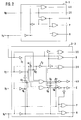
- Fig. 1 is a circuit block diagram showing an embodiment of the present invention. There is shown an example of the multiplier for multiplying the multiplicand X (x o to x 15 ) of 16 bits and the multiplier Y (y 0 to y 15 ) of 16 bits.
- the circuit is constructed by applying an N-channel MOSIC technology. Incidentally, the operation is described in positive logic, but the negative logic is also acceptable.
- the multiplicand X is supplied to a 3X producing circuit 1 through input terminals (x 0 to x 15 ).
- the multiplier Y is received at input terminals (y 0 to y 15 ) and is divided into a plurality of bits (e.g., two bits y 0 and y 1 at the first stage of a decoder 3 and subsequently y 1 - y 4 , Y4 - y 7 , y 7 - y 10 , y 10 - Y 13 and y 13 - y 15 ), which are simultaneously applied to the corresponding stages 3-2 to 3-6, respectively.
- a shift/selector circuit 2 has a plurality of logic circuits 2 1 to 2 108 arranged in array shape. The logic circuits 2 18 , 2 36 ...
- the 3X producing circuit 1 is composed of sixteen blocks 1 1 to 1 16 and executes 2X + X by its shift operation and adding operation. Wherein, the LSB (x 0 ) of the multiplicand X is directly transferred to the logic circuit 2 18 in the shift/selector circuit 2.
- the block 1 1 at the left side of the 3X producing circuit 1 receives a low level signal (ground level signal) at an input terminal. Each block has the same element.
- the first stage 3-1 and the second stage 3-2 of the decoder are shown in Fig. 2. The decoding operation is executed according to the four bits of the multiplier Y at a time as shown in table 3.
- the decoder 3 generates six kinds of signals (0, X, 2X, 3X, 4X, P and N), where P and N mean the sign signals designating a positive value and a negative value, respectively. Further, since y -1 and y -2 are both "0", the y 0 and y l , the signals generated from the first stage 3-1 are only 0, ⁇ 2X and ⁇ 4X as shown in table 3. Therefore, by applying only y 0 and y 1 to the first stage 3-1 of the decoder 3, the circuit can be simplified. That is, in Fig.
- the transistor gate G 1 receives an output of an inverter I 1 at a gate electrode and its source (or drain) electrode is coupled to the y 2 , while its drain (or source) electrode is coupled to an inverter I 2 and to a source (or drain) electrode of the transistor gate G 2 .
- the sixth stage 3-6 receives the y 13 to y 15 and a ground level signal as same as the block 1 1 of the 3X producing circuit 1.
- the signal N of each stage is directly applied to the corresponding block 2 1 , 2 19 , 2 37 , 2 55 , 2 73 and 2 91 and is inverted by inverters 10 to 14 to correct the sign bit.
- the inverted signals N are applied to the adjacent blocks 2 19 to 2 91 , respectively.
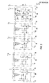
- the 3X producing circuit 1 is shown in detail in F ig. 3 in which 16 blocks 11 to 1 16 have the same circuit pattern. Each block has an AND gate 30 and a NOR gate 31 which receives the corresponding bit and the bit of the previous bit.
- a NOR gate 32 receives outputs of the AND gate 30 and the NOR gate 31 and generates a control signal for controlling a carry signal propagation. That is, the carry signal is propagated through a propagation line 34 which is elongated through all blocks.
- the control signal is applied at a gate electrode of a switching transistor gate G 33 . If x 0 and x 1 are all "0", the gate G 33 is turned off.
- the carry signal is stopped, but the signal (a ground level) designating no carry generation is transferred to the adjacent block 1 15 since the gate G 30 is turned on. While, if either x 0 or x 1 is "1", the gate G 33 is turned on, thereby the carry signal from the previous block is transferred to the adjacent block. Further, if y 1 and y 0 are all "1", the gate G 33 is turned off and the gate G 31 is turned on by an output "1" of NOR gate 33. Therefore, a carry signal generated by the block itself is transferred to the next block. As shown in Fi g. 3, the AND gate 30 and the NOR gate 31 receives the signal from the previous bit which is equal to the shifted bit by one (that is, 2X).
- each block receives 2X and X and adds to each other, thereby 3X is produced and is transferred to the shift/selector circuit 2 through line 36.
- the X is also directly transferred through line 35 to the shift/selector circuit 2.
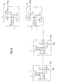
- the logic circuit 2 1 to 2 18 of the shift/selector circuit 2 are shown in Fig. 4. These circuits are defferent from the subsequent circuits 2 19 to 2 108 because the number of input signals from the decoder 3 is defferent from that of the circuits 2 19 to 2 108 .
- the circuits 2 1 to 2 18 includes four switching transistor gates G 40 to G 43 , an inverter 40 and a NOR gate 41, respectively.
- the gate G 40 is turned on in response to the signal 4X, as the result the multiplicand X shifted in the direction of left by two bits, that is 4X is selected and is transferred to the NOR gate 41.
- the one bit shifted multiplicand X that is, 2X is selected by the gate G 41 . Further, the selected data is transferred through line 42 to the lower logic circuits shown in Fig. 5 with the multiplicand X. In Fig. 5, the logic circuits 2 19 to 2 90 are omitted.
- the logic circuits in Fig. 5 receives the signals X, 2X, 3 X , 4X, 0, P and N from the decoder 3 for selecting the data 4X, 3X, 2X, X and C according to the decoding operation.
- the selecting operation is executed by four switching gate transistors G 50 and G 53 .
- a NAND gate 50, an AND gate 51 and NOR gates 52, 53 and 54 act as a full adder, and two output 55 and 56 are produced. Further, the signal N is used as the sign bit 57.
- Adder circuits 4 0 to 4 31 are shown in Fig. 6, in which each circuit pattern may be as same as that of Fig. 3.
- the product (total sum) of 32 bits are obtained at the output terminals P 0 to P 31 .
- the shift/selector circuit 2 executes the shift operation to produce partial products according to the result of the decoding operation, but it has not the 3X producing circuit. That is, the circuit 2 1 to 2 18 has only a selector (40, G 40 , G 41 ) and a zero-inversion control circuit (G 42 , G 43 and 41). Moreover, the remaining circuits 219 to 2 108 connected with the decoders 3-2 to 3-6 are made to have the same construction as that of the circuit 2 91 , which is equipped with a shift/selector means (G 50 to G 53 ), a zero-inversion control means (G 54 , G 55 and 54) and a full adder (50 to 53 and 60).
- a shift/selector means G 50 to G 53
- a zero-inversion control means G 54 , G 55 and 54
- a full adder 50 to 53 and 60.
- This full adder executes the operation of inverting the value of 4X, 2X, X or 3X, if these are negative (minus), to add 1 to the LSB. Moreover, the decoder 3 and the shift/selector circuit 2 are connected through a compensation circuit based upon the equation (11).
- the value 3X is generated in response to the input of the multiplicand X so that the two data X and 3X are supplied from the 3X generating circuit 1 to the shift/selector circuit 2. These data are selected and processed in accordance with the decoded results. The partial products thus generated are added in the final-stage adders 4 and 4' so that the products P 0 to P 31 of 32 bits are outputted.
- the multiplier can be decoded in 4 bits at a time so that a high-speed multiplier can be provided. Moreover, the generations of odd times (3X) are conducted simultaneously with the input of the multiplicand, and the selections of the values 3X and X are conducted in accordance with the decoded results. As a result, the multiplications can be easily executed by a small quantity of the hardware.
- the table of the ROM or the like prepared with the data of odd times of 3X or more may be used and referred in accordance with the decoded results.
- the basic construction may be composed of: the 3X generator which is separated from the circuit 2, the shifter means for generating 2X and 4X for the multiplicand X in accordance with the results of decoding an arbitrary group of the multiplier Y; the selector for selecting one of the values 3X, C, X, 2X and 4X; the inverter for inverting those values; the adder for adding the partial products thus generated; and the circuit for weighing in accordance with the multiplication groups (For example, a shift of each 3 bits is made to the MSB in the parallel system, whereas a shifter is required in the sequential system).
- the multiplier having its code bits overflown requires a circuit for temporarily holding the overflown bits, which can be eliminated from the present invention.
- the multiplier shown in Fig. 1 has other advantages to be enumerated in the following:
- the present multiplier can be constructed of a reduced number of elements and can have its critical path (i.e., its longest carry transmission path) shortened.
Landscapes
- Physics & Mathematics (AREA)
- General Physics & Mathematics (AREA)
- Engineering & Computer Science (AREA)
- Computational Mathematics (AREA)
- Mathematical Analysis (AREA)
- Mathematical Optimization (AREA)
- Pure & Applied Mathematics (AREA)
- Theoretical Computer Science (AREA)
- Computing Systems (AREA)
- General Engineering & Computer Science (AREA)
- Complex Calculations (AREA)
- Compression, Expansion, Code Conversion, And Decoders (AREA)
Applications Claiming Priority (2)
| Application Number | Priority Date | Filing Date | Title |
|---|---|---|---|
| JP17341/84 | 1984-02-02 | ||
| JP59017341A JPS60163128A (ja) | 1984-02-02 | 1984-02-02 | 乗算回路 |
Publications (2)
| Publication Number | Publication Date |
|---|---|
| EP0152046A2 true EP0152046A2 (fr) | 1985-08-21 |
| EP0152046A3 EP0152046A3 (fr) | 1986-05-07 |
Family
ID=11941351
Family Applications (1)
| Application Number | Title | Priority Date | Filing Date |
|---|---|---|---|
| EP85101133A Withdrawn EP0152046A3 (fr) | 1984-02-02 | 1985-02-04 | Circuit de multiplication |
Country Status (3)
| Country | Link |
|---|---|
| US (1) | US4718031A (fr) |
| EP (1) | EP0152046A3 (fr) |
| JP (1) | JPS60163128A (fr) |
Cited By (1)
| Publication number | Priority date | Publication date | Assignee | Title |
|---|---|---|---|---|
| EP0248166A3 (fr) * | 1986-05-27 | 1990-09-05 | International Business Machines Corporation | Multiplieur binaire à plusieurs bits |
Families Citing this family (23)
| Publication number | Priority date | Publication date | Assignee | Title |
|---|---|---|---|---|
| US4864529A (en) * | 1986-10-09 | 1989-09-05 | North American Philips Corporation | Fast multiplier architecture |
| US4841468A (en) * | 1987-03-20 | 1989-06-20 | Bipolar Integrated Technology, Inc. | High-speed digital multiplier architecture |
| US4887232A (en) * | 1987-05-15 | 1989-12-12 | Digital Equipment Corporation | Apparatus and method for performing a shift operation in a multiplier array circuit |
| JPS6461121A (en) * | 1987-08-31 | 1989-03-08 | Mitsubishi Electric Corp | Semiconductor integrated circuit |
| JP2585649B2 (ja) * | 1987-11-30 | 1997-02-26 | インデータシステムズ株式会社 | 除算回路 |
| DE68928248T2 (de) * | 1988-01-29 | 1998-01-08 | Texas Instruments Inc | Hochgeschwindigkeits-Multiplizierer |
| US5115408A (en) * | 1988-01-29 | 1992-05-19 | Texas Instruments Incorporated | High speed multiplier |
| US4972362A (en) * | 1988-06-17 | 1990-11-20 | Bipolar Integrated Technology, Inc. | Method and apparatus for implementing binary multiplication using booth type multiplication |
| US4926371A (en) * | 1988-12-28 | 1990-05-15 | International Business Machines Corporation | Two's complement multiplication with a sign magnitude multiplier |
| EP0466814A4 (en) * | 1989-04-10 | 1993-02-24 | Motorola Inc. | Integer divider circuit |
| US5020017A (en) * | 1989-04-10 | 1991-05-28 | Motorola, Inc. | Method and apparatus for obtaining the quotient of two numbers within one clock cycle |
| JPH02300930A (ja) * | 1989-05-16 | 1990-12-13 | Oki Electric Ind Co Ltd | 乗算回路 |
| JPH03167664A (ja) * | 1989-11-28 | 1991-07-19 | Nec Corp | マトリクス演算回路 |
| EP0461902B1 (fr) * | 1990-06-14 | 1998-12-23 | Canon Kabushiki Kaisha | Réseau neuronal |
| US5771186A (en) * | 1995-06-07 | 1998-06-23 | International Business Machines | System and method for multiplying in a data processing system |
| JP3351672B2 (ja) * | 1995-12-20 | 2002-12-03 | 株式会社東芝 | 加算器 |
| US5841684A (en) * | 1997-01-24 | 1998-11-24 | Vlsi Technology, Inc. | Method and apparatus for computer implemented constant multiplication with multipliers having repeated patterns including shifting of replicas and patterns having at least two digit positions with non-zero values |
| US6877022B1 (en) * | 2001-02-16 | 2005-04-05 | Texas Instruments Incorporated | Booth encoding circuit for a multiplier of a multiply-accumulate module |
| US7315879B2 (en) * | 2001-02-16 | 2008-01-01 | Texas Instruments Incorporated | Multiply-accumulate modules and parallel multipliers and methods of designing multiply-accumulate modules and parallel multipliers |
| JP4180024B2 (ja) * | 2004-07-09 | 2008-11-12 | Necエレクトロニクス株式会社 | 乗算剰余演算器及び情報処理装置 |
| JP4170267B2 (ja) * | 2004-07-09 | 2008-10-22 | Necエレクトロニクス株式会社 | 乗算剰余演算器及び情報処理装置 |
| US9032009B2 (en) * | 2013-03-11 | 2015-05-12 | Freescale Semicondutor, Inc. | Multiplier circuit |
| US11400980B2 (en) | 2020-06-04 | 2022-08-02 | Caterpillar Inc. | Rib-less hoist structure for truck body |
Family Cites Families (7)
| Publication number | Priority date | Publication date | Assignee | Title |
|---|---|---|---|---|
| US3123707A (en) * | 1960-03-18 | 1964-03-03 | Computing machines | |
| US3508038A (en) * | 1966-08-30 | 1970-04-21 | Ibm | Multiplying apparatus for performing division using successive approximate reciprocals of a divisor |
| US4031377A (en) * | 1975-08-25 | 1977-06-21 | Nippon Gakki Seizo Kabushiki Kaisha | Fast multiplier circuit employing shift circuitry responsive to two binary numbers the sum of which approximately equals the mantissa of the multiplier |
| JPS5578339A (en) * | 1978-12-09 | 1980-06-12 | Casio Comput Co Ltd | Multiplication system |
| JPS57141753A (en) * | 1981-02-25 | 1982-09-02 | Nec Corp | Multiplication circuit |
| JPS58119045A (ja) * | 1982-01-07 | 1983-07-15 | Hitachi Medical Corp | 高速固定数演算回路 |
| US4547862A (en) * | 1982-01-11 | 1985-10-15 | Trw Inc. | Monolithic fast fourier transform circuit |
-
1984
- 1984-02-02 JP JP59017341A patent/JPS60163128A/ja active Granted
-
1985
- 1985-02-04 EP EP85101133A patent/EP0152046A3/fr not_active Withdrawn
- 1985-02-04 US US06/697,652 patent/US4718031A/en not_active Expired - Lifetime
Cited By (1)
| Publication number | Priority date | Publication date | Assignee | Title |
|---|---|---|---|---|
| EP0248166A3 (fr) * | 1986-05-27 | 1990-09-05 | International Business Machines Corporation | Multiplieur binaire à plusieurs bits |
Also Published As
| Publication number | Publication date |
|---|---|
| EP0152046A3 (fr) | 1986-05-07 |
| JPS60163128A (ja) | 1985-08-26 |
| US4718031A (en) | 1988-01-05 |
| JPH0447849B2 (fr) | 1992-08-05 |
Similar Documents
| Publication | Publication Date | Title |
|---|---|---|
| EP0152046A2 (fr) | Circuit de multiplication | |
| US4825401A (en) | Functional dividable multiplier array circuit for multiplication of full words or simultaneous multiplication of two half words | |
| KR940002479B1 (ko) | 고속 디지탈 병렬승산기(multiplier) | |
| KR920007029B1 (ko) | X×y 비트 배열 배율기/어큐뮬레이터 회로 | |
| US5506799A (en) | Booth array multiplying circuit having carry correction | |
| EP0018519B1 (fr) | Dispositif de multiplication comprenant un additionneur à sauvegarde/propagation des retenues | |
| JP3244506B2 (ja) | 小型乗算器 | |
| US4623982A (en) | Conditional carry techniques for digital processors | |
| US5740095A (en) | Parallel multiplication logic circuit | |
| US4441158A (en) | Arithmetic operation circuit | |
| US4745570A (en) | Binary multibit multiplier | |
| US4748584A (en) | Parallel multiplier utilizing Booth's algorithm | |
| US4879677A (en) | Parallel adder circuit with sign bit decoder for multiplier | |
| KR100245944B1 (ko) | 승산장치 | |
| US4677583A (en) | Apparatus for decimal multiplication | |
| US5060183A (en) | Parallel multiplier circuit using matrices, including half and full adders | |
| US6183122B1 (en) | Multiplier sign extension | |
| US4866655A (en) | Arithmetic processor and divider using redundant signed digit | |
| EP0361886B1 (fr) | Unité de calcul à virgule flottante | |
| US4839848A (en) | Fast multiplier circuit incorporating parallel arrays of two-bit and three-bit adders | |
| US4706210A (en) | Guild array multiplier for binary numbers in two's complement notation | |
| US5781462A (en) | Multiplier circuitry with improved storage and transfer of booth control coefficients | |
| US5493522A (en) | Fast arithmetic modulo divider | |
| JPH0448255B2 (fr) | ||
| US5912904A (en) | Method for the production of an error correction parameter associated with the implementation of modular operations according to the Montgomery method |
Legal Events
| Date | Code | Title | Description |
|---|---|---|---|
| PUAI | Public reference made under article 153(3) epc to a published international application that has entered the european phase |
Free format text: ORIGINAL CODE: 0009012 |
|
| 17P | Request for examination filed |
Effective date: 19850204 |
|
| AK | Designated contracting states |
Designated state(s): DE FR GB |
|
| PUAL | Search report despatched |
Free format text: ORIGINAL CODE: 0009013 |
|
| AK | Designated contracting states |
Kind code of ref document: A3 Designated state(s): DE FR GB |
|
| 17Q | First examination report despatched |
Effective date: 19890113 |
|
| STAA | Information on the status of an ep patent application or granted ep patent |
Free format text: STATUS: THE APPLICATION IS DEEMED TO BE WITHDRAWN |
|
| 18D | Application deemed to be withdrawn |
Effective date: 19910507 |
|
| RIN1 | Information on inventor provided before grant (corrected) |
Inventor name: NUKIYAMA, TOMOJI |