EP0152151A1 - Breitbandiger Einstellverstärker - Google Patents
Breitbandiger Einstellverstärker Download PDFInfo
- Publication number
- EP0152151A1 EP0152151A1 EP85200164A EP85200164A EP0152151A1 EP 0152151 A1 EP0152151 A1 EP 0152151A1 EP 85200164 A EP85200164 A EP 85200164A EP 85200164 A EP85200164 A EP 85200164A EP 0152151 A1 EP0152151 A1 EP 0152151A1
- Authority
- EP
- European Patent Office
- Prior art keywords
- output
- amplifier
- input
- control amplifier
- signal
- Prior art date
- Legal status (The legal status is an assumption and is not a legal conclusion. Google has not performed a legal analysis and makes no representation as to the accuracy of the status listed.)
- Granted
Links
- 108010074506 Transfer Factor Proteins 0.000 claims description 7
- 230000008878 coupling Effects 0.000 claims description 5
- 238000010168 coupling process Methods 0.000 claims description 5
- 238000005859 coupling reaction Methods 0.000 claims description 5
- 230000001419 dependent effect Effects 0.000 abstract description 2
- 230000003287 optical effect Effects 0.000 abstract description 2
- 239000013307 optical fiber Substances 0.000 abstract description 2
- 239000003990 capacitor Substances 0.000 description 10
- 230000010363 phase shift Effects 0.000 description 6
- 238000010586 diagram Methods 0.000 description 2
- 230000005669 field effect Effects 0.000 description 2
Images


Classifications
-
- H—ELECTRICITY
- H04—ELECTRIC COMMUNICATION TECHNIQUE
- H04B—TRANSMISSION
- H04B3/00—Line transmission systems
- H04B3/02—Details
- H04B3/04—Control of transmission; Equalising
- H04B3/14—Control of transmission; Equalising characterised by the equalising network used
- H04B3/141—Control of transmission; Equalising characterised by the equalising network used using multiequalisers, e.g. bump, cosine, Bode
-
- H—ELECTRICITY
- H03—ELECTRONIC CIRCUITRY
- H03G—CONTROL OF AMPLIFICATION
- H03G3/00—Gain control in amplifiers or frequency changers
- H03G3/02—Manually-operated control
- H03G3/04—Manually-operated control in untuned amplifiers
- H03G3/10—Manually-operated control in untuned amplifiers having semiconductor devices
- H03G3/12—Manually-operated control in untuned amplifiers having semiconductor devices incorporating negative feedback
Definitions
- the invention relates to a broadband control amplifier, comprising an amplifier (4) whose input is connected to the output of a combining arrangement (3) and whose output is connected to the signal input (6) of a signal splitter (5) having a factory , a first output (8) of the signal splitter (5) being coupled to the output (12) of the control amplifier, a second output (7) of the signal splitter (5) being coupled via a network (11) to the output (12) of the control amplifier and also to a first input (2) of the combining device (3) a second input of which is coupled to the input (1) of the control amplifier.
- Control amplifiers of this type can be used, for example as input amplifiers in a receiver for use in optical fibre systems, to compensate for the length and temperature dependent attenuation of the optical link.
- a control amplifier of such a type is disclosed in United States Patent 4,219,788.
- This prior art control amplifier has the disadvantage that the open loop gain depends on the factor ⁇ of the signal splitter. This renders it impossible to produce a broadband control amplifier having a signal splitter in the negative feed back loop and having a wide control range.
- the invention has for its object to provide a solution for the above problem.
- the invention is characterized in that at least one of the coupling paths of the first output (8) and the second output (7) of the signal splitter (5) comprises a network (13,50) to compensate for the influence of the factor ⁇ of the signal splitter on the open loop gain of the control amplifier.
- reference numeral 3 denotes a combining arrangement whose + input is connected to the input 1 of the control amplifier.
- the output of the combining arrangement is connected to the input of an amplifier 4.
- the output of the amplifier 4 is connected to the signal input 6 of a signal splitters.
- An output 7 of the signal splitter 5 is connected via a network 11 having a transfer factor ⁇ ( ⁇ 1) to an input of an adder circuit 62, whose output is connected to an output 12 of the contr6l amplifier.
- An output 8 of the signal splitter 5 is connected to a further input of the adder circuit 62 and also via a network 60 having the transfer factor ⁇ ( ⁇ 1) to an input of an adder circuit 61.
- a further input of the adder circuit 61 is connected to the output 7 of the signal splitter 5.
- the output of the adder circuit 61 is connected to an input 2 of the combining arrangement 3.
- a control input 9 of the signal splitter 5 is connected to a source 10 supplying a variable control voltage.
- ⁇ is the factor which in response to the control signal from the source 10 splits the output signal x of the amplifier 4 into a portion 0( .x and (1- ⁇ ).x, where 0 ⁇ ⁇ ⁇ 1. If the gain u of the amplifier 4 is much greater than 1 then it holds with a proper approximation that
- the whole control range amounts to:
- Fig. 2 shows diagrammatically the variation of the open loop gain with the associated phase shift as a function of the frequency of an amplifier based on the principle shown in Fig. 1.
- the associated phase shift is represented by the line III.
- the Figure shows that in this situation the phase margin F is in this example ⁇ 60° at an open loop gain of O dB and that the gain margin is V ⁇ -73 dB at a O° phase shift. So in this situation the control amplifier is stable.
- the associated phase shift continues to be the line III if it is assumed that this phase shift is completely produced in the amplifier 4 of Fig. 1.
- Fig. 3 shows a measure by means of which the open loop gain can be made independent of the signal splitter factor ⁇ .
- a network 13 is provided between the output 7 of the signal splitter 5 and the input 2 of the combining arrangement.
- a signal equal to ei(MAX).1/ ⁇ is present at the output 7 of the signal splitter 5 at the highest input level at the output 7. So this is 1/ ⁇ times greater than the input signal, whilst the output signal amounts only to ei(MAX). ⁇ , and in principle causes an unnecessarily large drive in the control amplifier. If this should be prevented, then the network 13 having the transfer factor 13 can be advantageously replaced by a network in the other branch of the signal splitter 5, which has a transfer factor 1/ ⁇ .
- a network 50 is now provided between the output 8 of the signal splitter 5 and the output 12 of the control amplifier.
- the transfer factor of the network 50 is closen to be equal to 1/ ⁇ .
- a simple calculation demonstrates that the relations (7) and (4) hold for the transfer function from the input 1 to the output 12 of the control amplifier.
- the open loop gain now amounts to and consequently is independent of the factor ⁇ of the signal splitter.
- the output impedance does depends on the factor ⁇ . This may be objectionable for some applications.
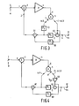
- Fig. 5 shows an embodiment in which both the open loop gain and the output impedance are independent of the factor ⁇ .
- An amplifier 18, which has unity gain, is dimensioned such that the input impedance is substantially - ⁇ , whilst the output impedance is substantially equal to O.
- An inverting input of the amplifier 4 is connected to the junction of a resistors 14, 15, 16 and the output 7 of the signal splitter 5.
- a non-inverting input of the amplifier 4 is connected to the input 1 of the control amplifier.
- the other terminal of the resistor 16 is connected to a point 100 of a constant potential.
- the other terminal of the resistor 15 is connected to the input of the amplifier 18 and also to the output 8 of the signal splitter 5.
- the resistor 17 is arranged between the input of the amplifier 18 and the point 100 of constant potential.
- the other terminal of the resistor 14 is connected to the output 12 of the amplifier 18.
- the output 12 of the amplifier 18 also constitutes the output of the control amplifier.
- control ranges are symmetrical. This indicates that at one extreme position of the control range the circuits amplify to exactly the same extent as they attenuate at the other extreme position.
- the control range can be made asymmetrical by adding an additional negative feedback networks. This feedback network can, for example, be arranged between the input 2 of the combining arrangement 3 and the network 11.
- the control range can be made asymmetrical by choosing the resistance values of the resistors 14 to 17 to be different from those indicated in the foregoing.
- Fig. 6 shows an detailed embodiment of the broadband control amplifier of Fig. 5.
- the input 1 of the control amplifier is connected to the gate electrode of a field effect transistor 23 via a coupling capacitor 20.
- the gate of the transistor 23 is connected to earth via the series arrangement of the resistor 21 and a capacitor 34.
- the source 2 is connected to the output 12 of the control amplifier via a series arrangement of a coupling capacitor 30 and a resistor 33.
- the source 2 is also connected to ground via a resistor 32.
- the drain of the field effect transistor 23 is connected to the positive pble of the supply voltage via a resistor 25 and also to the emitter of a transistor 24.
- the collector of transistor 24 is connected to the base electrode of a transistor 44 and also to the positive pole of the supply voltage via a resistor 26.
- the base electrode of the transistor 24 is connected to the positive pole of the supply voltage via the resistor and also to ground via the series arrangement of a resistor 29 and a diode 31.
- the base electrode of the transistor 24 is also connected to ground via a decoupling capacitor 28.
- the junction of the resistor 29 and the diode 31 is connected to the base electrode of a transistor 42, whose emitter is connected to the emitter of the transistor 44 via a resistor 43.
- the collector of the transistor 44 is connected to the junction of the emitter electrodes of a transistors 43 and 46.
- a variable voltage source 10 is arranged between the base electrode of the transistors 45 and 46.
- a d.c. voltage source 41 is arranged between the base electrode of the transistor 45 and ground.
- the collector of the transistor 45 is connected to the positive pole of the supply voltage via a resistor 50 and also to the base electrode of the transistor 35 via a coupling capacitor 47.
- the collector of the transistor 46 is connected via a resistor 49 to the positive pole of the supply voltage and also via a noupling capacitor 48 to the source of the transistor 23.
- a resistor 51 is provided between the collectors of the transistors 45 and 46.
- the collector of the transistor 42 is connected to the collector of a transistor 35 and also the junction of the resistor 21 and the capacitor 34.
- the emitter of the transistor 35 is connected to the output 12 of the control amplifier and also via a resistor 36 to the negative pole of the supply voltage.
- the series arrangement of a resistors 40 and 38 is provided between ground.and the negative pole of the supply voltage.
- the junction between the resistor 40 and 38 is connected via a resistor 39 to the base of the transistor 35 and also via a capacitor 37 to the emitter of the transistor 35.
- the output signal of the broadband control amplifier may alternatively be taken from the collector of the transistor 35. In that case a resistor is included between the point 101 and the collector of the transistor 35.
Landscapes
- Engineering & Computer Science (AREA)
- Computer Networks & Wireless Communication (AREA)
- Signal Processing (AREA)
- Amplifiers (AREA)
- Control Of Amplification And Gain Control (AREA)
- Networks Using Active Elements (AREA)
Applications Claiming Priority (2)
| Application Number | Priority Date | Filing Date | Title |
|---|---|---|---|
| NL8400463A NL8400463A (nl) | 1984-02-14 | 1984-02-14 | Breedband regelversterker. |
| NL8400463 | 1984-02-14 |
Publications (2)
| Publication Number | Publication Date |
|---|---|
| EP0152151A1 true EP0152151A1 (de) | 1985-08-21 |
| EP0152151B1 EP0152151B1 (de) | 1989-05-24 |
Family
ID=19843483
Family Applications (1)
| Application Number | Title | Priority Date | Filing Date |
|---|---|---|---|
| EP85200164A Expired EP0152151B1 (de) | 1984-02-14 | 1985-02-11 | Breitbandiger Einstellverstärker |
Country Status (6)
| Country | Link |
|---|---|
| US (1) | US4574253A (de) |
| EP (1) | EP0152151B1 (de) |
| JP (1) | JPS60187114A (de) |
| CA (1) | CA1223048A (de) |
| DE (1) | DE3570563D1 (de) |
| NL (1) | NL8400463A (de) |
Cited By (2)
| Publication number | Priority date | Publication date | Assignee | Title |
|---|---|---|---|---|
| EP0261739A1 (de) * | 1986-09-24 | 1988-03-30 | AT&T NETWORK SYSTEMS NEDERLAND B.V. | Kontrollverstärker |
| EP0262728A1 (de) * | 1986-09-24 | 1988-04-06 | AT&T NETWORK SYSTEMS NEDERLAND B.V. | Vorverstärker für einen optischen Empfänger |
Citations (2)
| Publication number | Priority date | Publication date | Assignee | Title |
|---|---|---|---|---|
| DE2233021B1 (de) * | 1972-07-05 | 1974-01-17 | Hahn-Meitner-Institut für Kernforschung Berlin GmbH, 1000 Berlin | Schaltungsanordnung zur konstanthaltung des frequenzgangs eines breitbandigen impulsverstaerkers mit aktiver verstaerkungseinstellung |
| US4219788A (en) * | 1978-10-24 | 1980-08-26 | Bell Telephone Laboratories, Incorporated | Active variable equalizer |
-
1984
- 1984-02-14 NL NL8400463A patent/NL8400463A/nl not_active Application Discontinuation
-
1985
- 1985-02-07 CA CA000473776A patent/CA1223048A/en not_active Expired
- 1985-02-11 DE DE8585200164T patent/DE3570563D1/de not_active Expired
- 1985-02-11 US US06/700,380 patent/US4574253A/en not_active Expired - Fee Related
- 1985-02-11 EP EP85200164A patent/EP0152151B1/de not_active Expired
- 1985-02-13 JP JP60024561A patent/JPS60187114A/ja active Granted
Patent Citations (2)
| Publication number | Priority date | Publication date | Assignee | Title |
|---|---|---|---|---|
| DE2233021B1 (de) * | 1972-07-05 | 1974-01-17 | Hahn-Meitner-Institut für Kernforschung Berlin GmbH, 1000 Berlin | Schaltungsanordnung zur konstanthaltung des frequenzgangs eines breitbandigen impulsverstaerkers mit aktiver verstaerkungseinstellung |
| US4219788A (en) * | 1978-10-24 | 1980-08-26 | Bell Telephone Laboratories, Incorporated | Active variable equalizer |
Non-Patent Citations (1)
| Title |
|---|
| PATENTS ABSTRACTS OF JAPAN, vol. 3, no. 103, 31st August 1979, page 84 E 134; & JP - A - 54 81753 (NIPPON DENKI) 29-06-1979 * |
Cited By (2)
| Publication number | Priority date | Publication date | Assignee | Title |
|---|---|---|---|---|
| EP0261739A1 (de) * | 1986-09-24 | 1988-03-30 | AT&T NETWORK SYSTEMS NEDERLAND B.V. | Kontrollverstärker |
| EP0262728A1 (de) * | 1986-09-24 | 1988-04-06 | AT&T NETWORK SYSTEMS NEDERLAND B.V. | Vorverstärker für einen optischen Empfänger |
Also Published As
| Publication number | Publication date |
|---|---|
| US4574253A (en) | 1986-03-04 |
| NL8400463A (nl) | 1985-09-02 |
| DE3570563D1 (en) | 1989-06-29 |
| JPH0535605B2 (de) | 1993-05-27 |
| CA1223048A (en) | 1987-06-16 |
| JPS60187114A (ja) | 1985-09-24 |
| EP0152151B1 (de) | 1989-05-24 |
Similar Documents
| Publication | Publication Date | Title |
|---|---|---|
| EP0181146B1 (de) | Transimpedanzverstärker | |
| US3684974A (en) | Automatic gain control rf-if amplifier | |
| US4514702A (en) | Logarithmic electronic gain control circuit | |
| JP2538938B2 (ja) | 光前置増幅器 | |
| US4590417A (en) | Voltage controlled diode attenuator | |
| KR840004327A (ko) | 신호 증폭 감쇄용 회로 | |
| US4567446A (en) | Light-receiving device for optical data transfer system | |
| US4956615A (en) | Input circuit for high-frequency amplifiers | |
| US4473780A (en) | Amplifier circuit and focus voltage supply circuit incorporating such an amplifier circuit | |
| EP0152151A1 (de) | Breitbandiger Einstellverstärker | |
| US4625131A (en) | Attenuator circuit | |
| US4250459A (en) | Circuit arrangement for automatic distortion correction of a signal | |
| KR0156923B1 (ko) | 증폭회로 | |
| KR900001117A (ko) | 자동 이득 제어회로 | |
| US4437070A (en) | Amplifier arrangement whose overall gain is controllable by means of a control voltage | |
| EP0115165B1 (de) | Aktive Lastschaltung | |
| US4099136A (en) | Amplifier circuit for high frequency signals, particularly for cable distribution systems, comprising at least a first transistor controlled at its base electrode by a signal source, and a difference amplifier | |
| US4663583A (en) | Automatically variable phase characteristic all-pass circuit | |
| EP0025950A1 (de) | Verstärkervorrichtung | |
| US4405903A (en) | Variolosser for an automatic gain control circuit | |
| US3405367A (en) | Quiescent current stabilized transistor amplifier | |
| KR910000373B1 (ko) | 가변 위상 보상 장치 | |
| EP0261739B1 (de) | Kontrollverstärker | |
| EP0337561A1 (de) | Regelverstärker | |
| JPS58117707A (ja) | 共通モ−ド信号の低減回路 |
Legal Events
| Date | Code | Title | Description |
|---|---|---|---|
| PUAI | Public reference made under article 153(3) epc to a published international application that has entered the european phase |
Free format text: ORIGINAL CODE: 0009012 |
|
| AK | Designated contracting states |
Designated state(s): DE FR GB SE |
|
| 17P | Request for examination filed |
Effective date: 19860219 |
|
| 17Q | First examination report despatched |
Effective date: 19870409 |
|
| GRAA | (expected) grant |
Free format text: ORIGINAL CODE: 0009210 |
|
| AK | Designated contracting states |
Kind code of ref document: B1 Designated state(s): DE FR GB SE |
|
| REF | Corresponds to: |
Ref document number: 3570563 Country of ref document: DE Date of ref document: 19890629 |
|
| ET | Fr: translation filed | ||
| PLBE | No opposition filed within time limit |
Free format text: ORIGINAL CODE: 0009261 |
|
| STAA | Information on the status of an ep patent application or granted ep patent |
Free format text: STATUS: NO OPPOSITION FILED WITHIN TIME LIMIT |
|
| 26N | No opposition filed | ||
| EAL | Se: european patent in force in sweden |
Ref document number: 85200164.3 |
|
| REG | Reference to a national code |
Ref country code: FR Ref legal event code: CD |
|
| PGFP | Annual fee paid to national office [announced via postgrant information from national office to epo] |
Ref country code: DE Payment date: 19960424 Year of fee payment: 12 |
|
| PGFP | Annual fee paid to national office [announced via postgrant information from national office to epo] |
Ref country code: GB Payment date: 19970203 Year of fee payment: 13 |
|
| PGFP | Annual fee paid to national office [announced via postgrant information from national office to epo] |
Ref country code: FR Payment date: 19970218 Year of fee payment: 13 |
|
| PGFP | Annual fee paid to national office [announced via postgrant information from national office to epo] |
Ref country code: SE Payment date: 19970225 Year of fee payment: 13 |
|
| PG25 | Lapsed in a contracting state [announced via postgrant information from national office to epo] |
Ref country code: DE Effective date: 19971101 |
|
| PG25 | Lapsed in a contracting state [announced via postgrant information from national office to epo] |
Ref country code: GB Free format text: LAPSE BECAUSE OF NON-PAYMENT OF DUE FEES Effective date: 19980211 |
|
| PG25 | Lapsed in a contracting state [announced via postgrant information from national office to epo] |
Ref country code: SE Free format text: LAPSE BECAUSE OF NON-PAYMENT OF DUE FEES Effective date: 19980212 |
|
| PG25 | Lapsed in a contracting state [announced via postgrant information from national office to epo] |
Ref country code: FR Free format text: THE PATENT HAS BEEN ANNULLED BY A DECISION OF A NATIONAL AUTHORITY Effective date: 19980228 |
|
| GBPC | Gb: european patent ceased through non-payment of renewal fee |
Effective date: 19980211 |
|
| EUG | Se: european patent has lapsed |
Ref document number: 85200164.3 |
|
| REG | Reference to a national code |
Ref country code: FR Ref legal event code: ST |