EP0152582A2 - Régulateur électronique de tension - Google Patents
Régulateur électronique de tension Download PDFInfo
- Publication number
- EP0152582A2 EP0152582A2 EP84115212A EP84115212A EP0152582A2 EP 0152582 A2 EP0152582 A2 EP 0152582A2 EP 84115212 A EP84115212 A EP 84115212A EP 84115212 A EP84115212 A EP 84115212A EP 0152582 A2 EP0152582 A2 EP 0152582A2
- Authority
- EP
- European Patent Office
- Prior art keywords
- transistor
- voltage regulator
- voltage
- resistor
- reference element
- Prior art date
- Legal status (The legal status is an assumption and is not a legal conclusion. Google has not performed a legal analysis and makes no representation as to the accuracy of the status listed.)
- Granted
Links
Images
Classifications
-
- G—PHYSICS
- G05—CONTROLLING; REGULATING
- G05F—SYSTEMS FOR REGULATING ELECTRIC OR MAGNETIC VARIABLES
- G05F3/00—Non-retroactive systems for regulating electric variables by using an uncontrolled element, or an uncontrolled combination of elements, such element or such combination having self-regulating properties
- G05F3/02—Regulating voltage or current
- G05F3/08—Regulating voltage or current wherein the variable is DC
- G05F3/10—Regulating voltage or current wherein the variable is DC using uncontrolled devices with non-linear characteristics
- G05F3/16—Regulating voltage or current wherein the variable is DC using uncontrolled devices with non-linear characteristics being semiconductor devices
- G05F3/18—Regulating voltage or current wherein the variable is DC using uncontrolled devices with non-linear characteristics being semiconductor devices using Zener diodes
Definitions
- the invention is based on an electronic voltage regulator according to the type specified in the preamble of claim 1.
- the electronic voltage regulator according to the invention with the characterizing features of claim 1 has the advantage that it provides a largely constant output voltage, which is temperature-stable, based on the positive potential of the operating voltage source. Another advantage is that the voltage regulator according to the invention manages with a relatively low operating current.
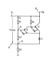
- An electronic voltage regulator according to the invention according to the figure has a voltage divider composed of three resistors R1, R2, R3 between its first connection 10, which is connected to the positive pole of the operating voltage source, and ground. Between the resistors R1 and R2 there is a first tap 11 which is connected to the base of a first transistor Tl of the pnp type. The emitter of the first transistor is connected firstly via a resistor R4 to the first connection 10 and secondly to the base of a second transistor T2 of the NPN type, the collector of which is also connected to the first connection 10.
- the collector of the first transistor T1 and the emitter of the second transistor T2 lead together to the cathode of a reference element E, the anode of which is connected to a second tap 12 located between the resistors R2 and R3.
- the circuit arrangement described above performs the following control functions. If, for example, the operating voltage U B for the voltage regulator rises, a higher current I S flows through the resistors Rl, R2, R3 of the voltage divider. The resulting higher voltage drop across resistor R2 controls the first transistor T1 in the conductive state. As a result, there is a current flow through the resistor R3 and the reference element E. The resulting voltage drop across the resistor R3 causes the potential to rise in the positive direction. The voltage available at the connections 13 and 14 thus remains largely constant with the appropriate dimensioning of the circuit arrangement.
- the transistors T1 and T2 are a complementary pair of transistors, the base-emitter voltages U BE of which change in the opposite direction when the temperature changes.
- Suitable complementary transistors are, for example, a transistor pair of the type BCW 61 D specially selected for this purpose for the transistor T1 and BCW 60 D for the transistor T2.
- the reference element is preferably of the MPS 5010 type.
- the resistance value of the resistor R1 is preferably equal to twice the resistance value of the resistor R2. If the voltage divider is supplemented accordingly, the voltage regulator can advantageously be used for supplying voltage to an integrated driver stage for a liquid crystal display (LCD display) which works according to the multiplex principle.
- LCD display liquid crystal display
Landscapes
- Physics & Mathematics (AREA)
- Engineering & Computer Science (AREA)
- Nonlinear Science (AREA)
- Electromagnetism (AREA)
- General Physics & Mathematics (AREA)
- Radar, Positioning & Navigation (AREA)
- Automation & Control Theory (AREA)
- Continuous-Control Power Sources That Use Transistors (AREA)
- Ignition Installations For Internal Combustion Engines (AREA)
- Details Of Television Scanning (AREA)
- Control Of Eletrric Generators (AREA)
- Control Of Electrical Variables (AREA)
Priority Applications (1)
| Application Number | Priority Date | Filing Date | Title |
|---|---|---|---|
| AT84115212T ATE43926T1 (de) | 1984-02-17 | 1984-12-12 | Elektronischer spannungsregler. |
Applications Claiming Priority (2)
| Application Number | Priority Date | Filing Date | Title |
|---|---|---|---|
| DE19843405661 DE3405661A1 (de) | 1984-02-17 | 1984-02-17 | Elektronischer spannungsregler |
| DE3405661 | 1984-02-17 |
Publications (3)
| Publication Number | Publication Date |
|---|---|
| EP0152582A2 true EP0152582A2 (fr) | 1985-08-28 |
| EP0152582A3 EP0152582A3 (en) | 1985-10-16 |
| EP0152582B1 EP0152582B1 (fr) | 1989-06-07 |
Family
ID=6227972
Family Applications (1)
| Application Number | Title | Priority Date | Filing Date |
|---|---|---|---|
| EP84115212A Expired EP0152582B1 (fr) | 1984-02-17 | 1984-12-12 | Régulateur électronique de tension |
Country Status (4)
| Country | Link |
|---|---|
| EP (1) | EP0152582B1 (fr) |
| JP (1) | JPH063565B2 (fr) |
| AT (1) | ATE43926T1 (fr) |
| DE (2) | DE3405661A1 (fr) |
Cited By (2)
| Publication number | Priority date | Publication date | Assignee | Title |
|---|---|---|---|---|
| GB2238890A (en) * | 1989-10-24 | 1991-06-12 | Samsung Electronics Co Ltd | Circuit for stabilizing a reference voltage |
| EP1898391A1 (fr) * | 2006-09-11 | 2008-03-12 | Samsung SDI Co., Ltd. | Affichage plasma et générateur de tension associé |
Families Citing this family (1)
| Publication number | Priority date | Publication date | Assignee | Title |
|---|---|---|---|---|
| DE4131170A1 (de) * | 1991-09-19 | 1993-03-25 | Telefunken Electronic Gmbh | Vorrichtung zur erzeugung von zwischenspannungen |
Family Cites Families (1)
| Publication number | Priority date | Publication date | Assignee | Title |
|---|---|---|---|---|
| DE1538440B2 (de) * | 1966-11-23 | 1972-03-16 | Deutsche Itt Industries Gmbh, 7800 Freiburg | Schaltungsanordnung zur gleichspannungsstabilisierung nach art einer z diode |
-
1984
- 1984-02-17 DE DE19843405661 patent/DE3405661A1/de not_active Withdrawn
- 1984-12-12 DE DE8484115212T patent/DE3478650D1/de not_active Expired
- 1984-12-12 EP EP84115212A patent/EP0152582B1/fr not_active Expired
- 1984-12-12 AT AT84115212T patent/ATE43926T1/de not_active IP Right Cessation
-
1985
- 1985-02-18 JP JP60028506A patent/JPH063565B2/ja not_active Expired - Lifetime
Cited By (2)
| Publication number | Priority date | Publication date | Assignee | Title |
|---|---|---|---|---|
| GB2238890A (en) * | 1989-10-24 | 1991-06-12 | Samsung Electronics Co Ltd | Circuit for stabilizing a reference voltage |
| EP1898391A1 (fr) * | 2006-09-11 | 2008-03-12 | Samsung SDI Co., Ltd. | Affichage plasma et générateur de tension associé |
Also Published As
| Publication number | Publication date |
|---|---|
| ATE43926T1 (de) | 1989-06-15 |
| DE3478650D1 (en) | 1989-07-13 |
| DE3405661A1 (de) | 1985-08-22 |
| JPS60189521A (ja) | 1985-09-27 |
| EP0152582A3 (en) | 1985-10-16 |
| JPH063565B2 (ja) | 1994-01-12 |
| EP0152582B1 (fr) | 1989-06-07 |
Similar Documents
| Publication | Publication Date | Title |
|---|---|---|
| EP0281684B1 (fr) | Commutateur à transistors Darlington protégé contre des surtensions | |
| DE69423121T2 (de) | Temperaturkompensierter Spannungsregler | |
| DE2154904B2 (de) | Temperaturkompensierte Bezugsgleichspannungsquelle | |
| DE69221999T2 (de) | Bezugsstromschleife | |
| EP0216265B1 (fr) | Circuit pour générer une tension de référence comportant une dérive en température prévisible | |
| DE3447002C2 (fr) | ||
| DE2250625A1 (de) | Stromregler | |
| DE3047685A1 (de) | Temperaturstabile spannungsquelle | |
| EP0152582A2 (fr) | Régulateur électronique de tension | |
| WO2001067594A1 (fr) | Circuit permettant de regler le point de fonctionnement d'un transistor haute frequence et montage amplificateur | |
| DE3716577C2 (de) | Stromspiegelschaltung großer Leistungsfähigkeit | |
| EP0904576A1 (fr) | Montage d'alimentation en courant | |
| DE1638010C3 (de) | Festkörperschaltkreis für Referenzverstärker | |
| DE3010618C2 (fr) | ||
| DE1948178B2 (de) | Aus einer Vielzahl individueller logischer Kreise bestehende monolithische Halbleiterschaltung mit integrierter Gleichspannungsstabilisierungs-Halbleiterschaltung | |
| DE3311258C1 (de) | Schaltungsanordnung zur UEberwachung einer Betriebsspannung | |
| DE3505635C2 (fr) | ||
| DE3127889A1 (de) | Schaltungsanordnung aus mindestens zwei verstaerkern | |
| EP0014351A2 (fr) | Porte NAND monolithiquement intégrable | |
| DE1934223A1 (de) | Schaltungsanordnung zum Erzeugen einer stabilisierten Gleichspannung | |
| DE2148880A1 (de) | Stromquelle | |
| DE3409417C2 (de) | Niederfrequenz-Verstärker | |
| DE69517948T2 (de) | Schaltkreis zum Vorspannen von epitaxialen Gebieten | |
| DE2437700A1 (de) | Schaltungsanordnung zur erzeugung von zwei konstanten spannungen | |
| WO1987007792A1 (fr) | Dispositif de protection contre les signaux parasites |
Legal Events
| Date | Code | Title | Description |
|---|---|---|---|
| PUAI | Public reference made under article 153(3) epc to a published international application that has entered the european phase |
Free format text: ORIGINAL CODE: 0009012 |
|
| PUAL | Search report despatched |
Free format text: ORIGINAL CODE: 0009013 |
|
| AK | Designated contracting states |
Designated state(s): AT DE FR GB |
|
| AK | Designated contracting states |
Designated state(s): AT DE FR GB |
|
| 17P | Request for examination filed |
Effective date: 19860122 |
|
| 17Q | First examination report despatched |
Effective date: 19871214 |
|
| GRAA | (expected) grant |
Free format text: ORIGINAL CODE: 0009210 |
|
| AK | Designated contracting states |
Kind code of ref document: B1 Designated state(s): AT DE FR GB |
|
| REF | Corresponds to: |
Ref document number: 43926 Country of ref document: AT Date of ref document: 19890615 Kind code of ref document: T |
|
| GBT | Gb: translation of ep patent filed (gb section 77(6)(a)/1977) | ||
| REF | Corresponds to: |
Ref document number: 3478650 Country of ref document: DE Date of ref document: 19890713 |
|
| ET | Fr: translation filed | ||
| PLBE | No opposition filed within time limit |
Free format text: ORIGINAL CODE: 0009261 |
|
| STAA | Information on the status of an ep patent application or granted ep patent |
Free format text: STATUS: NO OPPOSITION FILED WITHIN TIME LIMIT |
|
| 26N | No opposition filed | ||
| PGFP | Annual fee paid to national office [announced via postgrant information from national office to epo] |
Ref country code: DE Payment date: 19920831 Year of fee payment: 9 |
|
| PGFP | Annual fee paid to national office [announced via postgrant information from national office to epo] |
Ref country code: AT Payment date: 19921030 Year of fee payment: 9 |
|
| PGFP | Annual fee paid to national office [announced via postgrant information from national office to epo] |
Ref country code: GB Payment date: 19921202 Year of fee payment: 9 |
|
| PGFP | Annual fee paid to national office [announced via postgrant information from national office to epo] |
Ref country code: FR Payment date: 19930429 Year of fee payment: 9 |
|
| PG25 | Lapsed in a contracting state [announced via postgrant information from national office to epo] |
Ref country code: GB Effective date: 19931212 Ref country code: AT Effective date: 19931212 |
|
| GBPC | Gb: european patent ceased through non-payment of renewal fee |
Effective date: 19931212 |
|
| PG25 | Lapsed in a contracting state [announced via postgrant information from national office to epo] |
Ref country code: FR Effective date: 19940831 |
|
| PG25 | Lapsed in a contracting state [announced via postgrant information from national office to epo] |
Ref country code: DE Effective date: 19940901 |
|
| REG | Reference to a national code |
Ref country code: FR Ref legal event code: ST |