EP0152827A2 - Flüssigkristallfarbanzeigevorrichtung - Google Patents
Flüssigkristallfarbanzeigevorrichtung Download PDFInfo
- Publication number
- EP0152827A2 EP0152827A2 EP85100951A EP85100951A EP0152827A2 EP 0152827 A2 EP0152827 A2 EP 0152827A2 EP 85100951 A EP85100951 A EP 85100951A EP 85100951 A EP85100951 A EP 85100951A EP 0152827 A2 EP0152827 A2 EP 0152827A2
- Authority
- EP
- European Patent Office
- Prior art keywords
- liquid crystal
- color
- display apparatus
- crystal display
- accordance
- Prior art date
- Legal status (The legal status is an assumption and is not a legal conclusion. Google has not performed a legal analysis and makes no representation as to the accuracy of the status listed.)
- Granted
Links
Images








Classifications
-
- G—PHYSICS
- G02—OPTICS
- G02F—OPTICAL DEVICES OR ARRANGEMENTS FOR THE CONTROL OF LIGHT BY MODIFICATION OF THE OPTICAL PROPERTIES OF THE MEDIA OF THE ELEMENTS INVOLVED THEREIN; NON-LINEAR OPTICS; FREQUENCY-CHANGING OF LIGHT; OPTICAL LOGIC ELEMENTS; OPTICAL ANALOGUE/DIGITAL CONVERTERS
- G02F1/00—Devices or arrangements for the control of the intensity, colour, phase, polarisation or direction of light arriving from an independent light source, e.g. switching, gating or modulating; Non-linear optics
- G02F1/01—Devices or arrangements for the control of the intensity, colour, phase, polarisation or direction of light arriving from an independent light source, e.g. switching, gating or modulating; Non-linear optics for the control of the intensity, phase, polarisation or colour
- G02F1/13—Devices or arrangements for the control of the intensity, colour, phase, polarisation or direction of light arriving from an independent light source, e.g. switching, gating or modulating; Non-linear optics for the control of the intensity, phase, polarisation or colour based on liquid crystals, e.g. single liquid crystal display cells
- G02F1/137—Devices or arrangements for the control of the intensity, colour, phase, polarisation or direction of light arriving from an independent light source, e.g. switching, gating or modulating; Non-linear optics for the control of the intensity, phase, polarisation or colour based on liquid crystals, e.g. single liquid crystal display cells characterised by the electro-optical or magneto-optical effect, e.g. field-induced phase transition, orientation effect, guest-host interaction or dynamic scattering
- G02F1/139—Devices or arrangements for the control of the intensity, colour, phase, polarisation or direction of light arriving from an independent light source, e.g. switching, gating or modulating; Non-linear optics for the control of the intensity, phase, polarisation or colour based on liquid crystals, e.g. single liquid crystal display cells characterised by the electro-optical or magneto-optical effect, e.g. field-induced phase transition, orientation effect, guest-host interaction or dynamic scattering based on orientation effects in which the liquid crystal remains transparent
- G02F1/1396—Devices or arrangements for the control of the intensity, colour, phase, polarisation or direction of light arriving from an independent light source, e.g. switching, gating or modulating; Non-linear optics for the control of the intensity, phase, polarisation or colour based on liquid crystals, e.g. single liquid crystal display cells characterised by the electro-optical or magneto-optical effect, e.g. field-induced phase transition, orientation effect, guest-host interaction or dynamic scattering based on orientation effects in which the liquid crystal remains transparent the liquid crystal being selectively controlled between a twisted state and a non-twisted state, e.g. TN-LC cell
-
- G—PHYSICS
- G02—OPTICS
- G02F—OPTICAL DEVICES OR ARRANGEMENTS FOR THE CONTROL OF LIGHT BY MODIFICATION OF THE OPTICAL PROPERTIES OF THE MEDIA OF THE ELEMENTS INVOLVED THEREIN; NON-LINEAR OPTICS; FREQUENCY-CHANGING OF LIGHT; OPTICAL LOGIC ELEMENTS; OPTICAL ANALOGUE/DIGITAL CONVERTERS
- G02F1/00—Devices or arrangements for the control of the intensity, colour, phase, polarisation or direction of light arriving from an independent light source, e.g. switching, gating or modulating; Non-linear optics
- G02F1/01—Devices or arrangements for the control of the intensity, colour, phase, polarisation or direction of light arriving from an independent light source, e.g. switching, gating or modulating; Non-linear optics for the control of the intensity, phase, polarisation or colour
- G02F1/13—Devices or arrangements for the control of the intensity, colour, phase, polarisation or direction of light arriving from an independent light source, e.g. switching, gating or modulating; Non-linear optics for the control of the intensity, phase, polarisation or colour based on liquid crystals, e.g. single liquid crystal display cells
- G02F1/133—Constructional arrangements; Operation of liquid crystal cells; Circuit arrangements
- G02F1/1333—Constructional arrangements; Manufacturing methods
- G02F1/133371—Cells with varying thickness of the liquid crystal layer
-
- G—PHYSICS
- G02—OPTICS
- G02F—OPTICAL DEVICES OR ARRANGEMENTS FOR THE CONTROL OF LIGHT BY MODIFICATION OF THE OPTICAL PROPERTIES OF THE MEDIA OF THE ELEMENTS INVOLVED THEREIN; NON-LINEAR OPTICS; FREQUENCY-CHANGING OF LIGHT; OPTICAL LOGIC ELEMENTS; OPTICAL ANALOGUE/DIGITAL CONVERTERS
- G02F1/00—Devices or arrangements for the control of the intensity, colour, phase, polarisation or direction of light arriving from an independent light source, e.g. switching, gating or modulating; Non-linear optics
- G02F1/01—Devices or arrangements for the control of the intensity, colour, phase, polarisation or direction of light arriving from an independent light source, e.g. switching, gating or modulating; Non-linear optics for the control of the intensity, phase, polarisation or colour
- G02F1/13—Devices or arrangements for the control of the intensity, colour, phase, polarisation or direction of light arriving from an independent light source, e.g. switching, gating or modulating; Non-linear optics for the control of the intensity, phase, polarisation or colour based on liquid crystals, e.g. single liquid crystal display cells
- G02F1/133—Constructional arrangements; Operation of liquid crystal cells; Circuit arrangements
- G02F1/1333—Constructional arrangements; Manufacturing methods
- G02F1/1335—Structural association of cells with optical devices, e.g. polarisers or reflectors
- G02F1/133509—Filters, e.g. light shielding masks
- G02F1/133514—Colour filters
Definitions
- the present invention relates to an improvement in a color liquid crystal display apparatus, and particularly concerns a color liquid crystal display apparatus having twisted nematic liquid crystal combined with a number of color filter elements.
- the present invention is usable for color picture display apparatus for a television receiver set, a monitor in a videotape recorder, a view finder of a television camera or a display apparatus of a computer terminal machine.
- a color liquid crystal display apparatus has such a characteristics as having small thickness, operable with low voltage power source and consumes very small power, and accordingly its market is large. Furthermore, demand is rapidly growing these years as a flat type display apparatus. Developing from the conventional monocolor type liquid crystal display apparatus, color liquid crystal display apparatuses which uses a number of color filter elements are about to be introduced into actual use.
- DSM dynamic scatterinc mode
- TN twisted nematic mode
- GH guest-host mode
- TN liquid crystal has a characteristic of small driving power, high contrast and bright display.
- R red
- G green
- B blue
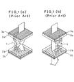
- FIG. 1 shows principle of display by transparent type TN liquid crystal display apparatus.
- a thick white arrow indicates direction of incident light and its polarization .
- the liquid crystal stops light as shown in FIG. l(a).
- V th a voltage above a threshold value
- the liquid crystal is realigned in the direction of the electric field (provided) that the dielectric constant anisotropy of the liquid crystal is positive), and incident light from the upper substrate passes through the liquid crystal apparatus. Accordingly by application or removal of voltage across the electrodes, contrast of brightness and darkness is obtainable.
- the above-mentioned type the liquid crystal apparatus wherein a dark state is represented at non-impression of voltage across the electrodes on both substrates is defined as"normally black" type.
- transmittance T at 0 volt impression is not 0.
- a linearly polarized light incident to the cell changes into elliptically polarized wave light and hence passes the cell.
- Transmittance of parallel light incident normally to the liquid crystal cell at the 0 volt impression state is given by the following equation (C.H.Gooch, H.A.Tarry: J.Phys.D:Appl.Phys.8,1575(1975)): wherein wherein d is thickness of the liquid crystal layer, An is defraction anisotropy of the liquid crystal, 6 is twist angle of the TN liquid crystal and X is wavelength of incident light.
- the defraction anisotropy An of the liquid crystal has a dependency on the wavelength of the incident light.
- FIG. 2 shows the wavelength-dependency of the defraction anisotropy an of a liquid crystal, for example, LIXON 9150 manufactured by Chisso Kabushiki Kaisha.
- FIG. 4 shows a sectional view of a conventional color liquid crystal display apparatus.
- the apparatus has a color filter having R, G and B color filter elements disposed in a matrices as shown in FIG. 5, and the apparatus has alignment films 6a and 6b formed on the inner wall of the substrate so as to control initial alignment of the liquid crystal at 0 volt impression state. Therefore by impressing a voltage above the threshold voltage V th across the transparent conductive film 5a and 5b, the molecular alignment of the liquid crystal is changed, so as to modulate light passing through the liquid crystal cell.
- FIG. 6 shows one example of spectral transmittance characteristic of the color filters of R, G and B color used in this conventional apparatus.
- the problems to consider are leak and undesirable coloring of light at 0 voltage impression. Since a contrast ratio is defined as [light transmittance for bright state] /[light transmittance for dark state], in the apparatus of the conventional configuration the existance of light leaking in the dark state, i.e., 0 volt impression state results in lowering of the contrast ratio.
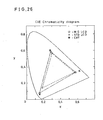
- the apparatus shows blue or violet color as a whole at the 0 voltage impression instead of a perfect black. This phenomenon is a grave obstacle in full color displaying by the color liquid crystal display apparatus.
- the purpose of the present invention is to provide an improved color liquid crystal display apparatus capable of disolving the above-mentioned problems of the conventional color liquid crystal display apparatus, thereby to minimize light leaking and resultant coloring of the color liquid crystal display apparatus at the 0 voltage impression and to achieve high contrast and good color performance for wide view angle of the color liquid crystal display apparatus.
- the color liquid crystal display apparatus in accordance with the present invention is featured by using TN mode liquid crystal layer combined with color filter elements of R, G and B colors wherein thickness of the liquid crystal layer is varied for respective parts of different color filters.
- the color liquid crystal display apparatus in accordance with the present invention comprises,
- a color display apparatus of transparent type using a TN mode liquid crystal is described in detail.
- the color filters of R, G and B those having spectral distribution of transmittance as shown by FIG. 6 is used in combination with a white color fluorescent lamp having such spectral energy distribution as shown in FIG. 7 made by Matsushita Electronic Corporation and given with a trade mark PA-LOOK are selected.
- the spectral energies of of R, G and B light energies are represented by the wavelength of 610 nm, 545 nm and 450 nm.
- the fluorescent lamp has a spectral characteristic of light like line spectra and give a color of light of white, and such spectral distribution of the light source is effective for the embodiment of the present invention, though the display apparatus in accordance with the present invention can be used with a continuous spectral light such as sunlight.
- the above-mentioned LIXON 9150 is used as the TN mode liquid crystal.
- the wavelength of the lights R, G and B shows transmittance as shown in FIG. 8 for variation of the thickness d of the liquid crystal layer in normally black type at 0 voltage impression state.
- the inventors made the following experimental study.
- the inventors made 18 kinds of sample cells having cell thicknesses as shown in the Table 1 and of NB type and NW type. That is, the eighteen samples are divided into two kinds of groups, namely, NB type and NW type, by selecting the directions of polarizer to be provided on the substrates. And spectral transmittances of these samples are measured for various applied voltages as parameter. Experimental results of the example are shown in FIG. 9(a) and FIG. 9(b).
- FIG. 10 shows response characteristics of the transmittance and applied voltage taking the wavelengths as parameters.
- lights of long wavelengths show relatively high transmittances at relatively low impressed voltages.
- the relatively thick cells as is shown by the inserted graph showing the left end parts of the curves enlarged, there is a undesirable phenomenon that the transmittance decreases as impressed voltage increases around the threshold voltage V th .
- this phenomenon will cause undesirable inversion of brightness of the image at the range of such low impressed voltages.
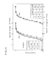
- FIG. 11 shows another example of dependency of light transmittance on impressed voltage.
- the curves of a group STD shows the transmittance of a cell having 5.2pm thickness liquid crystal layer, and the three curves correspond to the lights of the wavelengths of 610 nm, 545 nm and 450 nm.
- the relation between the transmittance and impressed voltage depends on the wavelengths is not uniquely defined by the impressed voltage.
- the curves designated by MG show light transmittances of the cells having 4,1, 5.2 and 5.7 ⁇ m thick for lights having the wavelengths of 450 nm, 545 nm and 610 nm, respectively. From the comparison experimental results shown in FIG.
- transmittance of the liquid crystal cell having a uniform liquid crystal layer thickness at 0 volt impression is calculated by the below mentioned equation (5).
- T FR is spectral transmittance of red filter as illustrated in FIG. 6.
- R, G and B represent red, green and blue color.
- FIG. 12 shows result of the calculation, wherein curve MG shows the results of the multi-gap liquid crystal cell embodying the present invention calculated by equation (4), and the curve STD shows the result of the comparison example of the conventional apparatus calculated by the equation (5). As is obvious from the curves of FIG.
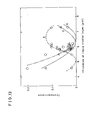
- the dotted line curve P shows a calculation result induced from the equation (1) by taking account of dependency on defractive index of the liquid crystal.
- a straight line Q shows a calculation result induced from the equation (1) by setting An equal 0.1.
- measurement result of the ⁇ min shows good agreement with these calculated results.
- a chain line S of F IG. 14 shows average values of distribution of ⁇ min when the liquid crystal cell is illuminated by scatter light. Inventors' many experiments showed that the result points distribute with a width of the gap between the curve P and the chain line S around this chain line S.
- the liquid crystal layer thickness d of the display apparatus is preferred to be designed from the value shown by the chain line S. Accordingly, as shown by the summary of the invention, as a measure to make differences in the liquid crystal layer thickness, such a configuration of forming terraced surfaces on at least one of substrate which constitutes the liquid crystal cell is adopted. Once central wavelengths of three colors are decided, gaps between terraced surfaces on the parts of the filter elements of blue and green and the difference for green and red parts, namely ⁇ d GB and ⁇ d GR ,can be easily obtained from FIG. 14. As is obvious from FIG.
- optimum terraced surface gap for the case of parallel light illumination ( ⁇ d BG(P) , ⁇ d GR(P) ) and optimum terraced surface gap for the scatter light illumination ( ⁇ d BG(S)' ⁇ d GR(S) ) show almost analogous values.
- the terraced surface gap is strictly designed and so worked in manufacturing, this does not necessarily requires very strict limitation. That is, if the relations of the terraced surface gaps are made to correspond to relation of wavelength of the central lights of the filter elements, the technical advantages of the present invention is effectively performed in comparison with the conventional liquid crystal color display apparatus having a uniform liquid crystal layer.
- FIG. 15 A first example of a concrete configuration of the color liquid crystal display apparatus in accordance with the present invention is shown in a sectional side view FIG. 15 showing the cross section of a part of the apparatus.
- the color liquid crystal display apparatus comprising a cell having two substrates 2a and 2b disposed in parallel with a predetermined gap inbetween thereby forming a closed space the substrates 2a and 2b, which have poralizer layer 3a and 3b attached on outer surface thereof, respectively.
- the substrates 2a and 2b further have transparent conductive films 5a and 5b and further have alignment film 6a and 6b, respectively.
- color filter layer 4 is formed on the transparent substrate 2b and under the transparent conductive film 5b.
- the color filter layer 4 has different thicknesses for R part, G part and B part.
- the color filter 4 of a predetermined pattern As other method to form the color filter 4 of a predetermined pattern, a known process such as three time repetitions of coating of organic material containing gelatin as host material and containing a color dye is used. As other method, screen printing, vapour deposition of pigments and electrolyte coating, etc. may be used.
- the transparent conductive film 5b made of, for instance, In 2 0 3 of Sn0 2 are formed and the alignment film 6b is formed.
- the alignment film 6b usually such organic material as polyimide or polyvinylalcohol is coated by spinner process or printing, followed by surface lapping. As other method, an oblique vapour deposition of SiO film may be used. Then by assembling the first substrate 2a and the second substrate 2b in a manner that the gap d B becomes 3.7pm, then d G and d R are automatically made 4.8pm and 5.4pm, respectively. And a TN liquid crystal 1 is filled in the space formed by the first substrate 2a and the second substrate 2b.
- the poralizer 3a and 3b are disposed in a manner that the poralization axis becomes each other parallel and also parallel to the wrapping direction of the alignment film 6a and 6b.
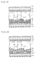
- a lower transparent substrate 2b has terraced surface having three levels formed in a predetermined pattern.
- FIG. 17 schematically shows perspective view of the lower substrate. A small part of the substrate is shown in enlarged size in FIG. 18.
- FIG. 18 is drawn by magnifying vertical size in about 100 times or more in order to show the terraced surfaces.
- the terraced transparent substrate 2b is made of a plastic material or glass and the terraced surface is formed by molding or by etching.
- B parts are formed on X-marked highest terrace
- G parts are formed on Y-marked medium height
- R parts are formed on Z-parts of lowest level.
- the plan view disposition of the color filter layer is, for instance as shown in FIG. 5.
- the forming of the color filter can be made by three times repetitions of coatings of organic materials, selective removal and dyeing. But other method, for instance printing, vapour deposition of pigment and electric field coating or other method may be used.
- the gap between the surfaces of the terraced of the substrate is at larget 1-2um, while length of the terrace is 100 times-1000 times, and therefore the transparent conductive film 5b and the alignment film 6b can be formed with continuity without any difficulty. Accordingly the alignment controlling of the liquid crystal has no difficulty.
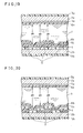
- a third actual example is described with reference to FIG. 19.
- the color filter layer 4 is directly formed on the inner surface of the substrate 2b, and thereon transparent film 7 with different thicknesses is formed.
- Other parts and components and steps of forming are similar to the forgoing examples.
- the transparent film 7 is formed on the parts G and B of the color filter layer 4 and the parts on the B filter element parts are made thicker.
- d R d G and d B to be 5.4pm, 4.8pm and 3.7 ⁇ m, respectively, for instance the transparent film 7 on the G part is formed 0.6pm while that on the B parts are 1.7pm.
- the material of the transparent film 7 a material having a good light transmittance in a visible light range (400 - 700 nm) and has a flat spectral transmittance characteristic is usable.
- Organic and inorganic material may be used.
- the coating is made by spinner coating, printing,vapour deposition or sputtering, and undesirable parts are selectively removed after forming. And by repeating the method, the above-mentioned transparent film having different thicknesses is made.
- the transparent film serves to realize the liquid crystal layer having optimum thicknesses. Therefore the transparent film 7 may be provided in other places, as shown in subsequent examples.
- the transparent film having parts of different thicknesses corresponding to the parts of different colors of the color filter layer 4 is formed between the substrate 2b and the color filter layer 4. That is, between the G parts of the color filter 4 and the substrate 2b thinner parts of the transparent film 7 is formed. And between the blue parts of the color filter parts 4 and the substrate 2b, thicker parts of the transparent film 7 are formed.
- Other parts and components of the apparatus are similar to those of the forgoing examples.
- the transparent film 7 is provided on all the filter elements for, G and B parts with different thickness corresponding to the color of the filter elements.
- the transparent film 7 is formed on the color filter 4 and under transparent conductive film 5b.
- the thicknesses of the transparent film 7 is O.lpm, 0.7pm and 1.8pm for the parts on the R parts, G parts and B parts of the color filter layer 4.
- Other parts and components and making steps are similar to the forgoing examples.
- FIG. 22 shows still another concrete example configuration wherein the transparent film 7 having different thicknesses for R parts, G parts and B parts of the color filter 4 is formed under the color filter 4 and on the substrate 2b.
- the relations of the thicknesses of the transparent film 7 is same as that of the example of FIG. 21.
- the color filter layer 4 and the transparent 7 are not necessarily each other independent configuration.
- the part corresponding to R filter elements are dyed by masking the parts to corresponds to G parts and B parts of the color filter layer 4, and then after masking the parts corresponding to the R parts and B parts the G color is dyed. And finally by masking the parts corresponding to R parts and G parts the B parts are dyed, thereby to form R, G and B dyed filter elements on the transparent film 7.
- transparent film preferably gelatin or the like organic film is appropriate.
- the color filter layer is described to have three kinds colors R, G and B only, but color filter may be of other type having four colors or different combination of colors are usable to embodying the present invention.
- the color filter layer is formed on only one substrate in the above-mentioned embodiments, the color filter layer may be formed on both substrate. For instance,some color element(s) are formed on one substrate and other color element(s) are formed on the other substrate.
- the thicknesses of the liquid crystal layer d R , d G and d in appropriate value in the rule described with reference to FIG. 14, the invention can be embodied.
- the concept of the present invention can be applicable for all kinds of color liquid crystal display apparatus utilizing TN liquid crystal, and therefore, the pattern of the color filter and the corresponding electrodes and the corresponding thickness pattern are not limited to the above-mentioned check pattern matrix, but also may be any pattern.
- the present invention is of course applicable to the liquid crystal display apparatus wherein MOSFET, TFT (thin film transistor), MIM (metal insulator metal) diode or the like non-linear or active element may be formed on at least one substrate.
- the embodiment is not limited to the transparent type display apparatus but of course is applicable also to reflection type display apparatus.
- the NB type is mainly described, but NW type is equally usable only by reversing the levels of the signal.
- the transmittances for red light and green light are small and for blue light is large.
- the thickness of the actually assembled apparatus becomes to 5.7pm (by increasing 0.5pm from the designed value)
- the transmittances for green color increases and for the blue color becomes maximum, thereby making the display panel more bluish.
- the thickness of the assembled apparatus becomes to 4.7pm (by decreasing 0.5pm from the designed value)
- the transmittances for blue light decreases and for red light increases, thereby making the display panel reddish.
- the conventional apparatus undesirably changes color in a great extent by shift of the thickness of only 0.5 ⁇ m.
- the liquid crystal cell embodying the present invention has a large tolerance for error of thicknesses in assembling. This is the very important fact and feature of the present invention.
- the inventors made a practical color liquid crystal display apparatus having liquid crystal layers with plural thicknesses for R, G and B parts of the color filter layer combined with amorphous silicon (hereinafter abreviated as a-Si) TFT for application in an image display panel.
- a-Si amorphous silicon
- Components of the image display panel such as TFT array, liquid crystal, poralizer, color filter layers, illumination system, electric circuit for imaging signal generation for operation of the image display panel, etc. have each particular characteristics or peculiar properties.
- the image display system should be designed and manufactured to achieve a high quality display as a combination of technology in the liquid crystal panel design, driving technology, etc. basing on the above-mentioned characteristics and peculiar properties.
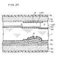
- FIGs. 27 and 28 Detailed cross sectional view and circuit diagram of a-Si TFT-addressed liquid crystal full color display panel is shown in FIGs. 27 and 28, respectively.
- the display panel comprises layer 4 of filter array and the a-Si TFT array as shown in FIG. 28 in the space between two substrate 2a and 2b to achieve an improvement of the display.
- black stripes 9 are formed on the part between neighboring color filter element parts, where no image signal is impressed, in order to shield unnecessary lights, to improve the contrast and color purity.
- light masking layer of light transmittance under 0.5% is formed to protect stable operation of the TFT 8.
- the above-mentioned trial manufacture display apparatus was experimented.
- the gap between terraced surfaces of the substrate to give difference of thicknesses of the liquid crystal layer is measured by a surface roughness meter.
- Thickness of the liquid crystal layer 1 confined in the space between the substrate 2a having the filter layer 4 and the substrate 2b having the array of a-Si TFT 8 are measured by interference method.
- Response characteristics of applyed voltage vs transmittances is measured as follows. White light from a halogen lamp is applied through optical fibers and an optical diffusion plate disposed on one face of the display panel to illuminate the latter.
- An input voltage of the driver is impressed across gate buses 20 and source buses 21 of TFT's array illustrated in FIG.
- Transmitted light through the display panel is received by light measuring optical fibers and guided to a photomultiplier.
- a band path filter having half width of 10 nm is inserted between the measuring optical fiber and the photomultiplier.
- the contrast is calculated as a ratio of the transmittance at impression of source voltage of 6 V rms and the transmittance of 0 V in this experiment, the transmitted lights are observed in a direction vertical to the display panel.
- the designed ideal gap between R and G parts is 0.6pm and the designed ideal gap between the G and B parts is 0.9pm.
- the above-mentioned color liquid crystal display apparatus comprises array of the TFT 8 of FIG. 28 consisting of 252 x 240 unit circuits corresponding to the picture elements, and a 2.4 inch diagonal size display panel combined with the above-mentioned color filter layer with plural depths is driven by AC voltage impression.
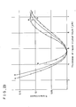
- the characteristic curve of input signal vs transmittance is shown in FIG. 24.
- the display apparatus of the above-mentioned experiment shows the characteristic shown by the curves MG of FIG.
- the contrast is above 30 for all range of the wavelengths of 460 nm to 700 nm. Especially, at the wavelengths of 630 nm and 560 nm, the relation between the thickness d and the wavelength of minimum transmission ⁇ min are well agreeing on the curve S of FIG. 14. Accordingly the contrast is above 100. For blue color, the contrast is relatively small. This is considered due to leaking of blue color light from the red filter. It is also considered that the reason of lowering aparent blue color contrast is due to simultaneous switching of picture elements of all colors of the liquid crystal.
- the present display panel can represent good natural colors without voltage compensation.
Landscapes
- Physics & Mathematics (AREA)
- Nonlinear Science (AREA)
- Chemical & Material Sciences (AREA)
- Crystallography & Structural Chemistry (AREA)
- General Physics & Mathematics (AREA)
- Optics & Photonics (AREA)
- Mathematical Physics (AREA)
- Liquid Crystal (AREA)
Applications Claiming Priority (6)
| Application Number | Priority Date | Filing Date | Title |
|---|---|---|---|
| JP16553/84 | 1984-01-31 | ||
| JP59016552A JPS60159823A (ja) | 1984-01-31 | 1984-01-31 | カラ−液晶表示装置 |
| JP59016554A JPS60159830A (ja) | 1984-01-31 | 1984-01-31 | カラ−液晶表示装置 |
| JP16554/84 | 1984-01-31 | ||
| JP16552/84 | 1984-01-31 | ||
| JP59016553A JPS60159824A (ja) | 1984-01-31 | 1984-01-31 | カラ−液晶表示装置 |
Publications (3)
| Publication Number | Publication Date |
|---|---|
| EP0152827A2 true EP0152827A2 (de) | 1985-08-28 |
| EP0152827A3 EP0152827A3 (en) | 1985-10-02 |
| EP0152827B1 EP0152827B1 (de) | 1989-10-18 |
Family
ID=27281454
Family Applications (1)
| Application Number | Title | Priority Date | Filing Date |
|---|---|---|---|
| EP85100951A Expired EP0152827B1 (de) | 1984-01-31 | 1985-01-30 | Flüssigkristallfarbanzeigevorrichtung |
Country Status (3)
| Country | Link |
|---|---|
| US (1) | US4632514A (de) |
| EP (1) | EP0152827B1 (de) |
| DE (1) | DE3573842D1 (de) |
Cited By (12)
| Publication number | Priority date | Publication date | Assignee | Title |
|---|---|---|---|---|
| EP0184003A3 (en) * | 1984-12-06 | 1988-04-27 | Vdo Adolf Schindling Ag | Liquid-crystal cell |
| DE3741995A1 (de) * | 1987-12-11 | 1989-06-22 | Vdo Schindling | Stn fluessigkristallzelle |
| EP0337711A1 (de) * | 1988-04-13 | 1989-10-18 | Ube Industries, Ltd. | Flüssigkristallanzeigevorrichtung |
| US4917471A (en) * | 1986-08-30 | 1990-04-17 | Canon Kabushiki Kaisha | Liquid crystal device |
| WO1990015360A1 (de) * | 1989-05-30 | 1990-12-13 | Hoechst Aktiengesellschaft | Ferroelektrisches flüssigkristalldisplay mit graustufen bzw. einer kontinuierlichen grauskala |
| EP0328329A3 (de) * | 1988-02-06 | 1991-01-16 | Sharp Kabushiki Kaisha | Flüssigkristall-Anzeigevorrichtung |
| US5061043A (en) * | 1988-12-24 | 1991-10-29 | Samsung Electron Devices Co., Ltd. | Color liquid crystal display device with a green dye |
| EP0433931A3 (en) * | 1989-12-18 | 1992-01-02 | Honeywell Inc. | Apparatus and method for a high contrast, wide angle, color, flat panel, liquid crystal display |
| US5250932A (en) * | 1988-04-13 | 1993-10-05 | Ube Industries, Ltd. | Liquid crystal display device |
| WO1996010775A1 (en) * | 1994-09-30 | 1996-04-11 | Honeywell Inc. | Wide-viewing angle multi-domain halftone active matrix liquid crystal display having compensating retardation |
| WO1998030931A1 (en) * | 1997-01-09 | 1998-07-16 | Tellium, Inc. | Wedge-shaped liquid-crystal cell |
| US7352419B2 (en) | 2003-12-10 | 2008-04-01 | Sharp Kabushiki Kaisha | Liquid crystal display having a control factor for reducing a chromaticity difference between displayed white and displayed black |
Families Citing this family (73)
| Publication number | Priority date | Publication date | Assignee | Title |
|---|---|---|---|---|
| US5196954A (en) * | 1985-08-08 | 1993-03-23 | Semiconductor Energy Laboratory Co., Ltd. | Liquid crystal display |
| EP0226218B1 (de) * | 1985-12-18 | 1993-07-14 | Canon Kabushiki Kaisha | Flüssigkristallvorrichtung |
| GB8604402D0 (en) * | 1986-02-21 | 1986-03-26 | Gen Electric Co Plc | Liquid crystal displays |
| US4802743A (en) * | 1986-03-20 | 1989-02-07 | Canon Kabushiki Kaisha | Liquid crystal device having color filters wherein the color filters formed from a polyamino resin containing coloring materials |
| EP0260712B1 (de) * | 1986-09-19 | 1995-12-27 | Matsushita Electric Industrial Co., Ltd. | Verfahren zur Herstellung eines Reliefstruktur ausgehärtetem Kunststoff auf einer transparenten, angefärbten Schicht |
| JPH0679122B2 (ja) * | 1986-10-22 | 1994-10-05 | セイコー電子工業株式会社 | 電気光学装置 |
| DE3751233T2 (de) * | 1986-10-31 | 1995-08-24 | Seiko Epson Corp | Anzeigevorrichtung vom Projektionstyp. |
| EP0277385A3 (en) * | 1987-01-27 | 1990-11-14 | Agfa-Gevaert Naamloze Vennootschap | Process for the manufacture of a relief element |
| JPS63144617U (de) * | 1987-03-14 | 1988-09-22 | ||
| US4929060A (en) * | 1987-05-06 | 1990-05-29 | Casio Computer Co., Ltd. | Color liquid crystal display device |
| JP2605723B2 (ja) * | 1987-07-22 | 1997-04-30 | 日本電気株式会社 | 薄膜トランジスタアレー形液晶表示装置 |
| US5012274A (en) * | 1987-12-31 | 1991-04-30 | Eugene Dolgoff | Active matrix LCD image projection system |
| US5300942A (en) * | 1987-12-31 | 1994-04-05 | Projectavision Incorporated | High efficiency light valve projection system with decreased perception of spaces between pixels and/or hines |
| US5117224A (en) * | 1988-02-16 | 1992-05-26 | Casio Computer, Ltd. | Color liquid crystal display apparatus |
| US4924215A (en) * | 1988-04-12 | 1990-05-08 | Bell Communcations Research, Inc. | Flat panel color display comprising backlight assembly and ferroelectric liquid crystal shutter assembly |
| US4968120A (en) * | 1988-10-28 | 1990-11-06 | International Business Machines Corp. | Multicolor liquid crystal display |
| US5216414A (en) * | 1989-11-20 | 1993-06-01 | Sharp Kabushiki Kaisha | Color liquid crystal display device |
| US5237437A (en) * | 1989-12-18 | 1993-08-17 | Honeywell Inc. | Apparatus and method for a high contrast, wide angle, color, flat panel, liquid crystal display |
| JP3011993B2 (ja) * | 1990-10-26 | 2000-02-21 | 株式会社リコー | カラー液晶素子 |
| DE69225738T2 (de) * | 1991-03-27 | 1998-10-01 | Technology Co Ag | Flüssigkristallanzeigeelement und Projektionsanordnung unter Verwendung desselben |
| JP2888382B2 (ja) * | 1991-05-15 | 1999-05-10 | インターナショナル・ビジネス・マシーンズ・コーポレイション | 液晶表示装置並びにその駆動方法及び駆動装置 |
| US5402141A (en) * | 1992-03-11 | 1995-03-28 | Honeywell Inc. | Multigap liquid crystal color display with reduced image retention and flicker |
| JP3012421B2 (ja) * | 1993-02-08 | 2000-02-21 | シャープ株式会社 | 反射型液晶表示装置 |
| JP3144607B2 (ja) * | 1993-04-09 | 2001-03-12 | 富士写真フイルム株式会社 | 光スイッチング素子 |
| JP2932229B2 (ja) * | 1993-06-04 | 1999-08-09 | キヤノン株式会社 | 液晶表示素子 |
| JPH0772446A (ja) * | 1993-09-01 | 1995-03-17 | Sharp Corp | 表示システム |
| US5499126A (en) * | 1993-12-02 | 1996-03-12 | Ois Optical Imaging Systems, Inc. | Liquid crystal display with patterned retardation films |
| US5570214A (en) * | 1993-12-15 | 1996-10-29 | Ois Optical Imaging Systems, Inc. | Normally white twisted nematic LCD with retardation films on opposite sides of liquid crystal material for improved viewing zone |
| US5907378A (en) * | 1993-12-15 | 1999-05-25 | Ois Optical Imaging Systems, Inc. | Normally white twisted nematic liquid crystal display including retardation films for improving viewing characteristics |
| US5594568A (en) * | 1993-12-15 | 1997-01-14 | Ois Optical Imaging Systems, Inc. | LCD with a pair of retardation films on one side of normally white liquid crystal layer |
| US5576861A (en) * | 1993-12-15 | 1996-11-19 | Ois Optical Imaging Systems, Inc. | Liquid crystal display having a retarder with 100-200nm retardation and having high contrast viewing zone centered in positive or negative vertical region |
| US5757524A (en) * | 1994-04-12 | 1998-05-26 | Rockwell International | Normally white multigap twisted nematic liquid crystal display with reduced hue variation over viewing angle |
| US5745200A (en) * | 1994-04-28 | 1998-04-28 | Casio Computer Co., Ltd. | Color liquid crystal display device and liquid crystal display apparatus |
| JP3085633B2 (ja) * | 1994-11-08 | 2000-09-11 | シャープ株式会社 | 反射型液晶表示装置 |
| US5638200A (en) * | 1995-02-03 | 1997-06-10 | Ois Optical Imaging Systems, Inc. | Liquid crystal display with tilted retardation film |
| US6137560A (en) * | 1995-10-23 | 2000-10-24 | Hitachi, Ltd. | Active matrix type liquid crystal display apparatus with light source color compensation |
| JPH09292504A (ja) * | 1996-02-27 | 1997-11-11 | Sharp Corp | 反射板及びその作製方法及びその反射板を用いた反射型液晶表示装置 |
| US6008875A (en) * | 1996-04-30 | 1999-12-28 | Nec Corporation | TN-mode liquid crystal display wherein a leveling layer is formed on the surface of an uneven electrode |
| CN1100279C (zh) * | 1996-10-29 | 2003-01-29 | 日本电气株式会社 | 有源矩阵液晶显示屏 |
| US5929955A (en) * | 1996-10-31 | 1999-07-27 | Industrial Technology Research Institute | Color LCD with microcompensators and macrocompensator |
| US5907380A (en) * | 1997-10-30 | 1999-05-25 | International Business Machines Corporation | Liquid crystal cell employing thin wall for pre-tilt control |
| US6037084A (en) * | 1998-08-12 | 2000-03-14 | Industrial Technology Research Institute | Method of making a color filter plate with multi-gap for LCD |
| EP1045272A3 (de) * | 1999-04-12 | 2004-02-25 | Matsushita Electric Industrial Co., Ltd. | Reflektive Farb-Flüssigkristall-Anzeigevorrichtung |
| JP3683172B2 (ja) * | 2000-11-09 | 2005-08-17 | シャープ株式会社 | 液晶表示素子 |
| US6809791B2 (en) * | 2001-02-01 | 2004-10-26 | Lg.Philips Lcd Co., Ltd. | Transflective liquid crystal display device having a color filter and method for fabricating thereof |
| US7123277B2 (en) | 2001-05-09 | 2006-10-17 | Clairvoyante, Inc. | Conversion of a sub-pixel format data to another sub-pixel data format |
| KR100759978B1 (ko) * | 2001-07-12 | 2007-09-18 | 삼성전자주식회사 | 수직 배향형 액정 표시 장치 및 그에 사용되는 색 필터 기판 |
| JP4050119B2 (ja) * | 2001-10-02 | 2008-02-20 | シャープ株式会社 | 液晶表示装置 |
| JP4368096B2 (ja) * | 2001-10-02 | 2009-11-18 | シャープ株式会社 | 液晶表示装置 |
| US7755652B2 (en) | 2002-01-07 | 2010-07-13 | Samsung Electronics Co., Ltd. | Color flat panel display sub-pixel rendering and driver configuration for sub-pixel arrangements with split sub-pixels |
| US7417648B2 (en) | 2002-01-07 | 2008-08-26 | Samsung Electronics Co. Ltd., | Color flat panel display sub-pixel arrangements and layouts for sub-pixel rendering with split blue sub-pixels |
| US7583279B2 (en) * | 2004-04-09 | 2009-09-01 | Samsung Electronics Co., Ltd. | Subpixel layouts and arrangements for high brightness displays |
| US20040051724A1 (en) * | 2002-09-13 | 2004-03-18 | Elliott Candice Hellen Brown | Four color arrangements of emitters for subpixel rendering |
| US7492379B2 (en) | 2002-01-07 | 2009-02-17 | Samsung Electronics Co., Ltd. | Color flat panel display sub-pixel arrangements and layouts for sub-pixel rendering with increased modulation transfer function response |
| JP3900077B2 (ja) * | 2002-12-10 | 2007-04-04 | セイコーエプソン株式会社 | カラーフィルタ基板、カラーフィルタ基板の製造方法、電気光学装置、電気光学装置の製造方法、及び、電子機器 |
| US7791679B2 (en) | 2003-06-06 | 2010-09-07 | Samsung Electronics Co., Ltd. | Alternative thin film transistors for liquid crystal displays |
| JP4089631B2 (ja) * | 2003-09-16 | 2008-05-28 | ソニー株式会社 | 液晶表示装置およびその製造方法 |
| JP4436161B2 (ja) * | 2004-03-12 | 2010-03-24 | 富士通株式会社 | 液晶表示装置 |
| US7248268B2 (en) | 2004-04-09 | 2007-07-24 | Clairvoyante, Inc | Subpixel rendering filters for high brightness subpixel layouts |
| US7573551B2 (en) | 2004-05-21 | 2009-08-11 | Sanyo Electric Co., Ltd. | Transflective liquid crystal display device and color liquid crystal display device |
| US7554623B2 (en) * | 2005-02-18 | 2009-06-30 | Infocus Corporation | Optical assembly to provide complementary illumination of subpixels of a light valve pixel |
| US7705855B2 (en) * | 2005-06-15 | 2010-04-27 | Samsung Electronics Co., Ltd. | Bichromatic display |
| KR101030529B1 (ko) * | 2005-06-20 | 2011-04-26 | 엘지디스플레이 주식회사 | 액정표시소자의 제조방법 |
| US7795653B2 (en) * | 2005-12-27 | 2010-09-14 | E. I. Du Pont De Nemours And Company | Electronic device including space-apart radiation regions and a process for forming the same |
| US7876341B2 (en) | 2006-08-28 | 2011-01-25 | Samsung Electronics Co., Ltd. | Subpixel layouts for high brightness displays and systems |
| US8018476B2 (en) | 2006-08-28 | 2011-09-13 | Samsung Electronics Co., Ltd. | Subpixel layouts for high brightness displays and systems |
| TWI375820B (en) * | 2008-02-27 | 2012-11-01 | Wintek Corp | Color filter with touch screen and liquid crystal display having the same |
| JP5560962B2 (ja) * | 2010-06-30 | 2014-07-30 | ソニー株式会社 | 液晶表示装置 |
| CN203259680U (zh) * | 2013-05-15 | 2013-10-30 | 京东方科技集团股份有限公司 | 彩色滤光片及显示装置 |
| TWI536083B (zh) | 2013-09-11 | 2016-06-01 | 友達光電股份有限公司 | 液晶面板及液晶顯示裝置 |
| CN104166258B (zh) * | 2014-08-18 | 2017-02-15 | 深圳市华星光电技术有限公司 | 液晶面板的灰阶值设定方法以及液晶显示器 |
| US10845665B1 (en) * | 2016-02-01 | 2020-11-24 | Apple Inc. | Devices with guest-host liquid crystal modulators |
| KR102632165B1 (ko) * | 2018-07-10 | 2024-02-01 | 삼성디스플레이 주식회사 | 표시 장치 및 그 제조 방법 |
Family Cites Families (5)
| Publication number | Priority date | Publication date | Assignee | Title |
|---|---|---|---|---|
| GB1264894A (de) * | 1968-06-17 | 1972-02-23 | ||
| US4006968A (en) * | 1975-05-02 | 1977-02-08 | Hughes Aircraft Company | Liquid crystal dot color display |
| IL60156A (en) * | 1980-05-25 | 1984-11-30 | Stolov Michael | Large electronically controlled liquid crystal display of one or more colors |
| US4387965A (en) * | 1981-01-06 | 1983-06-14 | Sharp Kabushiki Kaisha | Guest host type, positive and negative recessed liquid crystal display devices |
| JPS59180525A (ja) * | 1983-03-31 | 1984-10-13 | Citizen Watch Co Ltd | カラ−液晶表示パネル |
-
1985
- 1985-01-29 US US06/696,170 patent/US4632514A/en not_active Expired - Lifetime
- 1985-01-30 DE DE8585100951T patent/DE3573842D1/de not_active Expired
- 1985-01-30 EP EP85100951A patent/EP0152827B1/de not_active Expired
Cited By (21)
| Publication number | Priority date | Publication date | Assignee | Title |
|---|---|---|---|---|
| EP0184003A3 (en) * | 1984-12-06 | 1988-04-27 | Vdo Adolf Schindling Ag | Liquid-crystal cell |
| US5500751A (en) * | 1986-08-30 | 1996-03-19 | Canon Kabushiki Kaisha | Ferroelectric liquid crystal color filter surrounded by a heat fusible resin |
| US4917471A (en) * | 1986-08-30 | 1990-04-17 | Canon Kabushiki Kaisha | Liquid crystal device |
| US5568293A (en) * | 1986-08-30 | 1996-10-22 | Canon Kabushiki Kaisha | Liquid crystal display having trapezoidal color filters formed from a low-temperature curing polyamino resin having a photosensitive group |
| US5548424A (en) * | 1986-08-30 | 1996-08-20 | Canon Kabushiki Kaisha | Liquid crystal device having two resins films formed from solutions of different viscosities |
| DE3741995A1 (de) * | 1987-12-11 | 1989-06-22 | Vdo Schindling | Stn fluessigkristallzelle |
| DE3741995B4 (de) * | 1987-12-11 | 2004-10-28 | Siemens Ag | STN Flüssigkristallzelle |
| EP0328329A3 (de) * | 1988-02-06 | 1991-01-16 | Sharp Kabushiki Kaisha | Flüssigkristall-Anzeigevorrichtung |
| US5073772A (en) * | 1988-02-06 | 1991-12-17 | Sharp Kabushiki Kaisha | Liquid crystal display device |
| EP0337711A1 (de) * | 1988-04-13 | 1989-10-18 | Ube Industries, Ltd. | Flüssigkristallanzeigevorrichtung |
| US5250932A (en) * | 1988-04-13 | 1993-10-05 | Ube Industries, Ltd. | Liquid crystal display device |
| US5070326A (en) * | 1988-04-13 | 1991-12-03 | Ube Industries Ltd. | Liquid crystal display device |
| US5061043A (en) * | 1988-12-24 | 1991-10-29 | Samsung Electron Devices Co., Ltd. | Color liquid crystal display device with a green dye |
| US5257122A (en) * | 1989-05-30 | 1993-10-26 | Hoechst Aktiengesellschaft | Ferroelectric liquid crystal display having gray steps or a continuous gray scale |
| WO1990015360A1 (de) * | 1989-05-30 | 1990-12-13 | Hoechst Aktiengesellschaft | Ferroelektrisches flüssigkristalldisplay mit graustufen bzw. einer kontinuierlichen grauskala |
| EP0433931A3 (en) * | 1989-12-18 | 1992-01-02 | Honeywell Inc. | Apparatus and method for a high contrast, wide angle, color, flat panel, liquid crystal display |
| WO1996010775A1 (en) * | 1994-09-30 | 1996-04-11 | Honeywell Inc. | Wide-viewing angle multi-domain halftone active matrix liquid crystal display having compensating retardation |
| US5717474A (en) * | 1994-09-30 | 1998-02-10 | Honeywell Inc. | Wide-viewing angle multi-domain halftone active matrix liquid crystal display having compensating retardation |
| WO1998030931A1 (en) * | 1997-01-09 | 1998-07-16 | Tellium, Inc. | Wedge-shaped liquid-crystal cell |
| US7352419B2 (en) | 2003-12-10 | 2008-04-01 | Sharp Kabushiki Kaisha | Liquid crystal display having a control factor for reducing a chromaticity difference between displayed white and displayed black |
| CN100430781C (zh) * | 2003-12-10 | 2008-11-05 | 夏普株式会社 | 液晶显示器 |
Also Published As
| Publication number | Publication date |
|---|---|
| EP0152827A3 (en) | 1985-10-02 |
| EP0152827B1 (de) | 1989-10-18 |
| US4632514A (en) | 1986-12-30 |
| DE3573842D1 (en) | 1989-11-23 |
Similar Documents
| Publication | Publication Date | Title |
|---|---|---|
| US4632514A (en) | Color liquid crystal display apparatus | |
| US5753937A (en) | Color liquid crystal display device having a semitransparent layer on the inner surface of one of the substrates | |
| US5734455A (en) | Reflective birefringent type color liquid crystal display employing black mask | |
| US6624860B1 (en) | Color filter layer providing transmitted light with improved brightness and display device using same | |
| US6215538B1 (en) | Liquid crystal display including both color filter and non-color filter regions for increasing brightness | |
| US5731858A (en) | Reflection type liquid crystal display device and method of manufacturing the same | |
| US5179457A (en) | Liquid crystal display device with birefringent film between the substrates of the liquid crystal | |
| US5724112A (en) | Color liquid crystal apparatus | |
| US7079206B2 (en) | Color filter substrate for transflective liquid crystal display device with particular diffusive buffer layers and method of manufacturing the same | |
| US7616277B2 (en) | Transflective LCD device having dual thickness color filter | |
| US7110067B2 (en) | Liquid crystal display with varying orientation film thickness and method for manufacturing the same | |
| KR0131015B1 (ko) | 액정표시 소자 | |
| JPH11202325A (ja) | 反射型液晶表示装置およびその製造方法 | |
| US5471331A (en) | Spatial light modulator element with amorphous film of germanium, carbon and silicon for light blocking layer | |
| KR100730356B1 (ko) | 컬러필터 및 이를 구비하는 액정표시장치 | |
| JPH0548888B2 (de) | ||
| KR100635947B1 (ko) | 컬러 필터 기판 및 이를 포함하는 액정 표시 장치 | |
| JPH05313158A (ja) | カラー液晶ディスプレイ | |
| KR920006145Y1 (ko) | 컬러액정 표시장치 | |
| JPH0330126B2 (de) | ||
| US7349044B2 (en) | Liquid crystal display assembly having the interference filter disposed corresponding exclusively to the green region | |
| Koseki et al. | Color filter for 10.4-in.-diagonal 4096-color thin-film-transistor liquid crystal displays | |
| JPH08220527A (ja) | カラーフィルタ基板とその製造方法および液晶表示装置 | |
| CN100376967C (zh) | 彩色滤光片以及具有该彩色滤光片的液晶显示装置 | |
| KR100523763B1 (ko) | 콜레스테릭 액정 컬러 필터를 포함한 액정 표시 장치 |
Legal Events
| Date | Code | Title | Description |
|---|---|---|---|
| PUAI | Public reference made under article 153(3) epc to a published international application that has entered the european phase |
Free format text: ORIGINAL CODE: 0009012 |
|
| PUAL | Search report despatched |
Free format text: ORIGINAL CODE: 0009013 |
|
| 17P | Request for examination filed |
Effective date: 19850226 |
|
| AK | Designated contracting states |
Designated state(s): DE FR GB |
|
| AK | Designated contracting states |
Designated state(s): DE FR GB |
|
| 17Q | First examination report despatched |
Effective date: 19870729 |
|
| GRAA | (expected) grant |
Free format text: ORIGINAL CODE: 0009210 |
|
| AK | Designated contracting states |
Kind code of ref document: B1 Designated state(s): DE FR GB |
|
| REF | Corresponds to: |
Ref document number: 3573842 Country of ref document: DE Date of ref document: 19891123 |
|
| ET | Fr: translation filed | ||
| PLBE | No opposition filed within time limit |
Free format text: ORIGINAL CODE: 0009261 |
|
| STAA | Information on the status of an ep patent application or granted ep patent |
Free format text: STATUS: NO OPPOSITION FILED WITHIN TIME LIMIT |
|
| 26N | No opposition filed | ||
| REG | Reference to a national code |
Ref country code: GB Ref legal event code: 746 Effective date: 19950224 |
|
| REG | Reference to a national code |
Ref country code: FR Ref legal event code: D6 |
|
| REG | Reference to a national code |
Ref country code: GB Ref legal event code: IF02 |
|
| PGFP | Annual fee paid to national office [announced via postgrant information from national office to epo] |
Ref country code: FR Payment date: 20040108 Year of fee payment: 20 |
|
| PGFP | Annual fee paid to national office [announced via postgrant information from national office to epo] |
Ref country code: GB Payment date: 20040128 Year of fee payment: 20 |
|
| PGFP | Annual fee paid to national office [announced via postgrant information from national office to epo] |
Ref country code: DE Payment date: 20040212 Year of fee payment: 20 |
|
| PG25 | Lapsed in a contracting state [announced via postgrant information from national office to epo] |
Ref country code: GB Free format text: LAPSE BECAUSE OF EXPIRATION OF PROTECTION Effective date: 20050129 |
|
| REG | Reference to a national code |
Ref country code: GB Ref legal event code: PE20 |