EP0153526A2 - Procédé de dépôt sous vide utilisant un dispositif d'alimentation continue de pnicture, notamment pour pulvérisation - Google Patents
Procédé de dépôt sous vide utilisant un dispositif d'alimentation continue de pnicture, notamment pour pulvérisation Download PDFInfo
- Publication number
- EP0153526A2 EP0153526A2 EP84304414A EP84304414A EP0153526A2 EP 0153526 A2 EP0153526 A2 EP 0153526A2 EP 84304414 A EP84304414 A EP 84304414A EP 84304414 A EP84304414 A EP 84304414A EP 0153526 A2 EP0153526 A2 EP 0153526A2
- Authority
- EP
- European Patent Office
- Prior art keywords
- pnictide
- film
- chamber
- inert gas
- vacuum
- Prior art date
- Legal status (The legal status is an assumption and is not a legal conclusion. Google has not performed a legal analysis and makes no representation as to the accuracy of the status listed.)
- Withdrawn
Links
Images


Classifications
-
- C—CHEMISTRY; METALLURGY
- C23—COATING METALLIC MATERIAL; COATING MATERIAL WITH METALLIC MATERIAL; CHEMICAL SURFACE TREATMENT; DIFFUSION TREATMENT OF METALLIC MATERIAL; COATING BY VACUUM EVAPORATION, BY SPUTTERING, BY ION IMPLANTATION OR BY CHEMICAL VAPOUR DEPOSITION, IN GENERAL; INHIBITING CORROSION OF METALLIC MATERIAL OR INCRUSTATION IN GENERAL
- C23C—COATING METALLIC MATERIAL; COATING MATERIAL WITH METALLIC MATERIAL; SURFACE TREATMENT OF METALLIC MATERIAL BY DIFFUSION INTO THE SURFACE, BY CHEMICAL CONVERSION OR SUBSTITUTION; COATING BY VACUUM EVAPORATION, BY SPUTTERING, BY ION IMPLANTATION OR BY CHEMICAL VAPOUR DEPOSITION, IN GENERAL
- C23C14/00—Coating by vacuum evaporation, by sputtering or by ion implantation of the coating forming material
- C23C14/22—Coating by vacuum evaporation, by sputtering or by ion implantation of the coating forming material characterised by the process of coating
- C23C14/34—Sputtering
-
- H—ELECTRICITY
- H10—SEMICONDUCTOR DEVICES; ELECTRIC SOLID-STATE DEVICES NOT OTHERWISE PROVIDED FOR
- H10P—GENERIC PROCESSES OR APPARATUS FOR THE MANUFACTURE OR TREATMENT OF DEVICES COVERED BY CLASS H10
- H10P50/00—Etching of wafers, substrates or parts of devices
Definitions
- This invention relates to vacuum deposition processes employing a continuous pnictide delivery system, particularly sputtering; it also relates to sputtered semiconducting films of pnictide material, particularly KP15, KP x wherein x ranges from 15 to infinity, phosphorus, InP, GaP and GaAs; to the production of electronic semiconductor devices, electro- optical devices, thin films, optical films and coatings; to III-V semiconductor devices and to the passivation and insulation thereof.
- III-V semiconductors with pnictide films, particularly phosphorus.
- One of the above-identified related applications discloses a continuous pnictide source and delivery system for chemical vapour deposition.
- Another object of the present invention is to provide such a continuous delivery system.
- a further object of the present invention is to provide such a source utilizing an inert carrier gas.
- a still further object of the present is to facilitate the deposition of films of pnictides, poly- pnictides and other pnictide compounds, particularly when the pnictide is phosphorus, by sputtering.
- Yet another object of the present invention is to control the local order of a sputtered pnictide film.
- a further object of the present invention is to deposit films of III-V materials, particularly InP, GaP and GaAs.
- the deposition chamber comprises sputtering apparatus, in particular RF sputtering apparatus.
- the present invention also provides a process for tne vacuum deposition of a pnictide film characterised in that it comprises passing an inert gas through heated pnictide and supplying the product gas to a vacuum chamber.
- Vacuum chamber pressure is preferably maintained at above 10 -4 Torr ( 1 .33 x 10 -2 Pa), more preferably above 10 -3 Torr (1.33 x 10 -1 Pa).
- the present process generally comprises sputtering in the vacuum chamber in the presence of a Pnictide species introduced in the carrier gas so as to deposit a pnictide film, which may be elemental or compound, on a substrate. If, a compound, it is preferably a III-V compound, such as InP or GaAs.
- the pnictide may be P, As or Sb.
- the film may be a poly- . pnosphide or KP x wherein x is at least 15.
- the pnictide may be a compound semiconductor.
- polypnictide films may be grown in a vacuum system only in the presence of excess pnictide. It has now been found that a continuous pnictide source may be employed to supply Pnictide 4 species carried in an inert gas into the sputterer to supply the excess pnictide species.
- indium phosphide film has been successfully grown on glass substrates and there is no reason why indium phosphide should not be grown epitaxially on indium phosphide crystals. Moreover, it should be possible to deposit and epitaxially grow other III-V materials, particularly GaAs, using this system.
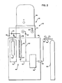
- apparatus for sputtering utilizing a continuous pnictide delivery system is generally indicated at 20. It comprises a vacuum chamber 22 maintained at a vacuum above 10 -4 Torr (1.33 x 10 -2 Pa), preferably above 10 -3 Torr (1.33 x 10⁻¹ Pa), and particularly in a range of from 2 to 3 x 10 -2 Torr (from 2.66 to 3.99 Pa). Plate electrodes 24 and 26 within the vacuum chamber 22 are connected to an RF power generator 28 providing from 5 to 250 watts of power at 13.56 megahertz.
- the vacuum chamber 22 contains argon gas as the sputtering medium.
- a pnictide delivery system 30 constructed in the manner disclosed in the above-identified related application based on USSN 581,102 is utilized to supply a stream of p nictide 4 vapour carried by argon gas in tube 32. This feeds a nozzle 34 having slots cut therein (not shown), to deliver the P 4 species as shown by the arrows 36. A source of argon gas is supplied to the pnictide bubbler as indicated by the arrow 38.
- the target 40 consisted of a pressed pellet of condensed phase KP 15 , as disclosed in the above-identified related application based on USSN 509,175 produced in the manner disclosed in GB-A-2,113,663 mentioned above.
- the pnictide bubbler was filled with liquid white phosphorus and the P 4 phosphorus species carried by the argon gas supplied to the bubbler at 38, exits the nozzle 34 in the dark space of the glow discharge below the target.
- the system is operated at a pressure of from 2 to 3 x 10 Torr (from 2.66 to 3.99 Pa).
- the peak voltage ranges from 50 to 2500 volts.
- the RF power range is from 5 to 250 watts.
- the bubbler temperature is maintained at from 50 to 150°C.
- the argon flow rate through the bubbler ranges from 5.5 to 65 standard cubic centimetres per minute.
- the pressure maintained in the pnictide source used ranges from atmospheric to subatmospheric.
- the flow rates of the P 4 species into the vacuum chamber 22 range from 2 x 10 6 to 6 x 10 -3 grams per minute.
- the substrates 26 have been maintained at temperatures ranging from 23 to 400°C. Deposition rates have varied from 2 to 250A ° (x10 -10 m) per minute.
- the P 4 system 36 is preferably directed upward into the dark space of the plasma where it is efficiently ionized and results in cracking of the P 4 species into various P species, which have a better sticking coefficient than P 4 and are required successfully to deposit polyphosphide films at the substrate 26.
- the apparatus 20 may be, for example, a Materials Research Corporation Model 86-20 RF diode sputterer comprising vacuum chamber base 42, chamber 44 and RF oil cover 46.
- the argon bubbler apparatus generally indicated at 48 comprises an argon supply cylinder 50, regulator 52, shutoff valve 54, micron (pm) filter 56 and hydrox gas purifier 58 to supply the argon gas to the RF sputterer on line 60 and through valve 62 and to supply the bubbler itself on line 63 through needle valve 64.
- the bubbler.apparatus 48 comprises a flow meter 66, pressure gauge 68, the bubbler 70 surrounded by a heated bath 72, inlet valve 74, outlet valve 76 and purge valve 78.
- Inlet needle valve 80 is utilized to control the ultimate flow rate into the vacuum chamber 22.
- Ternary, quaternary and other semiconductors having two differing pnictides require two independent pnictide delivery systems according to the present invention (one for each pnictide element) to be grown epitaxially in the glow discharge.
- These semiconductors comprising two metals require composite targets of the two metal compound semconductors which are to be grown.
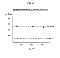
- the potassium deposition rate D K versus plasma power found in the present apparatus is linear with regard to plasma power and, as illustrated in accompanying Figure 4, does not vary with substate temperature.
- the phosphorus deposition rate Dp is a function of three variables, namely, the substrate temperature, the RF power and the rate of delivery of excess phosphorus to the system using the phosphorus bubbler. This may be seen from accompanying Figure 5. It may also be seen from accompanying Figure 5 that the deposition rate of phosphorus D in angstroms (10 -10 m) per minute is a linear function of power times excess phosphorus at a constant substrate temperature at low power.
- the composition of the polyphosphide deposited according to the present process by varying the substrate temperature.
- the polyphosphide films produced have a local order comprising highly disordered tubes. As the substrate temperature is raised, the tubes become more ordered.
- pnictides pnictide compounds
- polypnic- tides may be deposited according to the present invention.
- the total amount of energy supplied to the system comprising the substrate temperature and the RF power governs the local order obtained in the deposited films.
- the energy of the various cracked phosphorus species at the surface of the substrate must be very high for highly ordered microcrystalline structure to be obtained.
- the present apparatus and method may be used to supply other pnictides to a sputtering system and may be utilized to grow polycrystalline and crystalline films of compound or intermetallic semiconductors comprising a pnictide.
- the epitaxial growth by the present process of layers of varying compound or intermetallic pnictide semiconductors is contemplated.
- III-V semiconductors as used herein means those semiconductors commonly called intermetallic or compound, formed of compounds of elements from Group III and Group V of the Periodic Table, such as aluminium phosphide, aluminium arsenide, aluminium antimonide, gallium phosphide, gallium arsenide, gallium antimonide, indium phosphide, indium arsenide and indium antimonide and the ternary and quaternary semiconductors.
- pnictide is meant those elements from Group V of the Periodic Table, namely nitrogen, phosphorus, arsenic, antimony and bismuth.
Landscapes
- Chemical & Material Sciences (AREA)
- Chemical Kinetics & Catalysis (AREA)
- Engineering & Computer Science (AREA)
- Materials Engineering (AREA)
- Mechanical Engineering (AREA)
- Metallurgy (AREA)
- Organic Chemistry (AREA)
- Physical Vapour Deposition (AREA)
- Physical Deposition Of Substances That Are Components Of Semiconductor Devices (AREA)
- Formation Of Insulating Films (AREA)
- Chemical Vapour Deposition (AREA)
Applications Claiming Priority (2)
| Application Number | Priority Date | Filing Date | Title |
|---|---|---|---|
| US58110384A | 1984-02-17 | 1984-02-17 | |
| US581103 | 1984-02-17 |
Publications (2)
| Publication Number | Publication Date |
|---|---|
| EP0153526A2 true EP0153526A2 (fr) | 1985-09-04 |
| EP0153526A3 EP0153526A3 (fr) | 1986-06-18 |
Family
ID=24323896
Family Applications (1)
| Application Number | Title | Priority Date | Filing Date |
|---|---|---|---|
| EP84304414A Withdrawn EP0153526A3 (fr) | 1984-02-17 | 1984-06-28 | Procédé de dépôt sous vide utilisant un dispositif d'alimentation continue de pnicture, notamment pour pulvérisation |
Country Status (5)
| Country | Link |
|---|---|
| EP (1) | EP0153526A3 (fr) |
| JP (1) | JPS60178619A (fr) |
| KR (1) | KR850006257A (fr) |
| AU (1) | AU2993784A (fr) |
| DK (1) | DK318484A (fr) |
Family Cites Families (7)
| Publication number | Priority date | Publication date | Assignee | Title |
|---|---|---|---|---|
| US2503571A (en) * | 1947-05-02 | 1950-04-11 | Bell Telephone Labor Inc | Apparatus for coating surfaces by thermal vaporization at atmospheric pressure |
| DE1204494B (de) * | 1956-06-09 | 1965-11-04 | Siemens Ag | Verfahren und Vorrichtung zum Aufdampfen von Schichten aus einer bei Aufdampftemperatur nicht bestaendigen, als Halbleiter-Grundstoff verwendbaren Stoechiometrisch genaubestimmten Mehrstoffverbindung |
| FR1535167A (fr) * | 1967-08-24 | 1968-08-02 | Schloemann Ag | Procédé et dispositif de dégazage en continu de matériaux métalliques de revêtement |
| BE728917A (fr) * | 1968-02-28 | 1969-08-01 | ||
| DE2848331A1 (de) * | 1978-11-08 | 1980-05-22 | Philips Patentverwaltung | Verfahren zum herstellen von halbleiterbauelementen |
| US4430183A (en) * | 1980-10-30 | 1984-02-07 | The United States Of America As Represented By The United States Department Of Energy | Method of making coherent multilayer crystals |
| AU553091B2 (en) * | 1981-12-30 | 1986-07-03 | Stauffer Chemical Company | High phosphorus pholyphosphides |
-
1984
- 1984-06-27 AU AU29937/84A patent/AU2993784A/en not_active Abandoned
- 1984-06-28 EP EP84304414A patent/EP0153526A3/fr not_active Withdrawn
- 1984-06-28 DK DK318484A patent/DK318484A/da not_active Application Discontinuation
- 1984-06-29 JP JP59133483A patent/JPS60178619A/ja active Pending
- 1984-06-29 KR KR1019840003745A patent/KR850006257A/ko not_active Abandoned
Also Published As
| Publication number | Publication date |
|---|---|
| JPS60178619A (ja) | 1985-09-12 |
| DK318484A (da) | 1985-08-18 |
| AU2993784A (en) | 1985-08-22 |
| KR850006257A (ko) | 1985-10-02 |
| EP0153526A3 (fr) | 1986-06-18 |
| DK318484D0 (da) | 1984-06-28 |
Similar Documents
| Publication | Publication Date | Title |
|---|---|---|
| US7176054B2 (en) | Method of forming a p-type group II-VI semiconductor crystal layer on a substrate | |
| US20070248515A1 (en) | System and Method for Forming Multi-Component Films | |
| US7842588B2 (en) | Group-III metal nitride and preparation thereof | |
| US4916089A (en) | Process for the epitaxial production of semiconductor stock material | |
| WO1996028585A1 (fr) | Ensemble d'evacuation de type pomme de douche permettant l'apport d'une vapeur de reactif source a un substrat et procede de depot chimique en phase vapeur correspondant | |
| US4636268A (en) | Chemical beam deposition method utilizing alkyl compounds in a carrier gas | |
| EP0127200B1 (fr) | Procédé pour la fabrication d'un dispositif semi-conducteur utilisant la technique des faisceaux moléculaires | |
| US4649024A (en) | Method for forming evaporated pnictide and alkali metal polypnictide films | |
| US4761300A (en) | Method of vacuum depostion of pnictide films on a substrate using a pnictide bubbler and a sputterer | |
| EP0810307B1 (fr) | Méthode pour la préparation d'un film semi-conducteur du type composé | |
| US5202283A (en) | Technique for doping MOCVD grown crystalline materials using free radical transport of the dopant species | |
| EP0153526A2 (fr) | Procédé de dépôt sous vide utilisant un dispositif d'alimentation continue de pnicture, notamment pour pulvérisation | |
| EP0386190B1 (fr) | Source de mercure elementaire pour deposition en phase gazeuse par procede chimique organometallique | |
| Herman et al. | Molecular beam epitaxy | |
| US5326424A (en) | Cubic boron nitride phosphide films | |
| EP0138963B1 (fr) | Source de dopant au diethylberilium pour couches semiconductrices epitaxiales a croissance par depot de vapeur chimique organique metallique (mocvd) | |
| US11280025B2 (en) | Vapor phase epitaxy method | |
| EP0138965B1 (fr) | Tetramethyltine utilise comme source de dopage pour le developpement mocvd de couches semiconductrices epitaxiales | |
| Greenwald et al. | Mocvd Erbium Sourcesa | |
| Benz II et al. | Chemical beam epitaxy of CdTe, HgTe, and HgCdTe | |
| EP0152668A2 (fr) | Procédé de dépôt sous vide élevé utilisant un dispositif d'alimentation continue de pnicture | |
| JPH0574710A (ja) | 半導体薄膜の成長方法 | |
| EP0451782A2 (fr) | Méthode pour la préparation d'un film supraconducteur en oxyde | |
| Schachter et al. | Amorphous Polyphosphide Thin Films Prepared by Sputtering | |
| Schachter et al. | Reactive sputtering of polyphosphide thin films by plasma cracking of P4 |
Legal Events
| Date | Code | Title | Description |
|---|---|---|---|
| PUAI | Public reference made under article 153(3) epc to a published international application that has entered the european phase |
Free format text: ORIGINAL CODE: 0009012 |
|
| AK | Designated contracting states |
Designated state(s): AT BE CH DE FR GB IT LI LU NL SE |
|
| PUAL | Search report despatched |
Free format text: ORIGINAL CODE: 0009013 |
|
| AK | Designated contracting states |
Kind code of ref document: A3 Designated state(s): AT BE CH DE FR GB IT LI LU NL SE |
|
| 17P | Request for examination filed |
Effective date: 19861125 |
|
| STAA | Information on the status of an ep patent application or granted ep patent |
Free format text: STATUS: THE APPLICATION HAS BEEN WITHDRAWN |
|
| 18W | Application withdrawn |
Withdrawal date: 19870820 |
|
| RIN1 | Information on inventor provided before grant (corrected) |
Inventor name: SCHACHTER, ROZALIE Inventor name: VISCOGLIOSI, MARCELLO |