EP0153789A2 - Adressage de mémoires de caractères pour l'affichage de données - Google Patents
Adressage de mémoires de caractères pour l'affichage de données Download PDFInfo
- Publication number
- EP0153789A2 EP0153789A2 EP85200223A EP85200223A EP0153789A2 EP 0153789 A2 EP0153789 A2 EP 0153789A2 EP 85200223 A EP85200223 A EP 85200223A EP 85200223 A EP85200223 A EP 85200223A EP 0153789 A2 EP0153789 A2 EP 0153789A2
- Authority
- EP
- European Patent Office
- Prior art keywords
- character
- memory
- display
- drcs
- address
- Prior art date
- Legal status (The legal status is an assumption and is not a legal conclusion. Google has not performed a legal analysis and makes no representation as to the accuracy of the status listed.)
- Withdrawn
Links
- 230000015654 memory Effects 0.000 title claims abstract description 99
- 239000011159 matrix material Substances 0.000 claims description 5
- 230000000306 recurrent effect Effects 0.000 claims description 4
- 230000004044 response Effects 0.000 claims description 2
- 239000013256 coordination polymer Substances 0.000 abstract description 4
- 230000004048 modification Effects 0.000 abstract 1
- 238000012986 modification Methods 0.000 abstract 1
- 230000005540 biological transmission Effects 0.000 description 5
- 230000008859 change Effects 0.000 description 3
- 238000000034 method Methods 0.000 description 3
- 101710177589 Asp/Glu-specific dipeptidyl-peptidase Proteins 0.000 description 2
- YFPJFKYCVYXDJK-UHFFFAOYSA-N Diphenylphosphine oxide Chemical compound C=1C=CC=CC=1[P+](=O)C1=CC=CC=C1 YFPJFKYCVYXDJK-UHFFFAOYSA-N 0.000 description 2
- 230000009471 action Effects 0.000 description 2
- 238000010586 diagram Methods 0.000 description 2
- 230000000694 effects Effects 0.000 description 1
- 230000008520 organization Effects 0.000 description 1
- 230000009467 reduction Effects 0.000 description 1
- 239000013598 vector Substances 0.000 description 1
Images


Classifications
-
- G—PHYSICS
- G09—EDUCATION; CRYPTOGRAPHY; DISPLAY; ADVERTISING; SEALS
- G09G—ARRANGEMENTS OR CIRCUITS FOR CONTROL OF INDICATING DEVICES USING STATIC MEANS TO PRESENT VARIABLE INFORMATION
- G09G5/00—Control arrangements or circuits for visual indicators common to cathode-ray tube indicators and other visual indicators
- G09G5/22—Control arrangements or circuits for visual indicators common to cathode-ray tube indicators and other visual indicators characterised by the display of characters or indicia using display control signals derived from coded signals representing the characters or indicia, e.g. with a character-code memory
- G09G5/222—Control of the character-code memory
- G09G5/225—Control of the character-code memory comprising a loadable character generator
Definitions
- This invention relates to data display arrangements of a type for displaying as an entity on the screen of a CRT (cathode ray tube) or other raster scan display device, a quantity of stored data which is accessed repeatedly for its display in a recurrent cycle of scanning lines, the displayed data being composed of discrete characters organized in character rows each comprising a plurality of character positions, and the shape of each discrete character being defined by selected dots of a dot matrix which constitutes a character format for the characters.
- Data display arrangements of the above type are used in a variety of different applications.
- one such data display arrangement is used in conjunction with telephone data services which offer a telephone subscriber having a suitable video terminal (incorporating the arrangement), the facility of access over the public telephone network to a data source from which data can be selected and transmitted to the subscriber's premises for display.
- telephone data services which offer a telephone subscriber having a suitable video terminal (incorporating the arrangement), the facility of access over the public telephone network to a data source from which data can be selected and transmitted to the subscriber's premises for display.
- Examples of this usuage are the British and German videotext services Prestel andstructure.
- a data display arrangement of the above type includes, in addition to the CRT or other raster scan display device, acquisition means for acquiring from a data source transmission information representing data selected for display, a display memory for storing digital codes derived from the transmission information, and character generator means for producing, from the stored digital codes, character generating signals for driving the display device to produce the data display.
- the character generator means normally includes a fixed character memory in which is stored character information identifying the available character shapes which can be displayed by the arrangement. This character information is addressed selectively in accordance with the stored digital codes in the display memory, and the information read out is used to produce the character generating signals for the data display. This selective addressing is effected synchronously with the scanning action of the display device, which scanning action may be effected with or without field interlacing.
- DRCS dynamically redefinable character sets
- DRCS characters can have any alpha-mosaic (including alpha-numeric) shape, so that the total possible number of different shapes that can be made available is limited only by the character format used.
- DRCS characters can be defined as elements for constructing with high resolution, graphics such as maps, and geometric and other drawings.
- DRCS character is to be construed to mean a character the character information for which can be transmitted from a data source to the arrangement for temporary storage therein to form part of an overall character memory.
- DRCS character set is to be construed to mean a set of DRCS characters).
- a data display arrangement of the above type in which the display is "character-based" i.e. the display is made up of discrete characters in specified positions
- received transmission information provides coded instructions for defining display elements such as vectors, arcs, circles, etc. These instructions are decoded as they are received into dot information for the display elements concerned, and this dot information is stored in the display memory for direct read-out to provide the display.
- This storage is in co-called "bit-map" form, each pixel (or dot) of the display being represented by at least one stored bit.
- the amount of storage used by the display memory for such a bit-map display is far greater than that required by the display memory for a character-based display for which whole character memory cells (e.g. a matrix of up to.120 pixels) at a time are identified in the display memory, rather than individual pixels.
- whole character memory cells e.g. a matrix of up to.120 pixels
- a data display arrangement of the type set forth above having a plurality of memory sections for storing DRCS character sets, and addressing means for addressing said memory sections one at a time to identify each memory section individually for the read-out of DRCS characters therefrom for display, is characterised in that said addressing means is operable to address a first one of said memory sections for a corresponding first portion of each line scanning period of the raster scan and is further operable to address others of said memory sections for. respective further corresponding portions of each said line scanning period, whereby DRCS characters stored in any one of said memory sections are available for display only in a particular sub-area or sub-areas of the total display area of the screen that that memory section is individually identified with by such addressing.
- the number of DRCS characters that can be stored in a memory section can be the same as the number of character positions contained in a sub-area.
- each DRCS character of a set stored in a memory section can be individually and uniquely associated with a respective character position in the sub-area concerned, which means that each character dot position of a DRCS character can be individually and uniquely associated with a respective pixel position of the character position concerned.
- two or more sub-areas of the total display area of the screen may "share" the same DRCS character set as stored in a single memory section, in the sense that any DRCS character of the set is available for display in any character position of any of these two or more sub-areas.
- This can achieve a reduction in the number of memory sections which is required, but at the expense of not now having sufficient DRCS characters to associate individually with each character position.
- the allocation of the DRCS characters can be such that each character position in fine detail parts of the display has an individual DRCS character uniquely associated with it, while character positions in non-detailed parts of the display share DRCS characters.
- the allocation of DRCS character sets can be further extended by providing at least one additional memory section which can accommodate an additional DRCS character set and which can be addressed by said addressing means such as to provide DRCS characters for display at any character position on the total display area of the screen.
- the video display terminal shown in Figure 1 has a modem 1 by which the terminal has access over a telephone line 2, (e.g. via a switched public telephone network) to a data source 3.
- a logic and processor circuit 4 provides the signals necessary to establish the telephone connection to the data source 3.
- the circuit 4 also includes data acquisition means for acquiring transmission information from the telephone line 2.
- a command key pad 5 provides user control instructions to the circuit 4.
- An address/data bus system 6 interconnects the circuit 4 with a display memory 7, a fixed character memory 8 (ROM) and a DRCS character memory 9 (RAM). Under the control of the circuit 4, digital codes derived from the received transmission information and pertaining to characters to be displayed are loaded onto the address/data bus system 6 and assigned to appropriate locations in the display memory 7" as display data.
- addressing means in the circuit 4 accesses the display data stored in the display memory 7 and uses it to address the character memories 8 and 9, as appropriate, to produce character dot information.
- Shift registers 10 receive this character dot information and use it to drive a colour look-up table 11 to produce therefrom digital colour codes which are applied to a digital-to-analogue converter 12.
- the output signals from the converter 12 are the RGB character generating signals required for driving a television monitor 13 to display on the screen thereof the characters represented by the display data.
- attribute logic 14 which contains control data relating to different display attributes, such as "flashing", "underlining”, “colour choice", “double height”, etc.
- the circuit 4 is responsive to the stored attribute data to initiate the relevant attribute control by the attribute logic 14, to implement the attribute(s) concerned for the character display.
- the attribute data also signifies whether associated character data pertains to a character in the character memory 8 or to a character in the DRCS character memory 9.
- the display data in the display memory 7 represents a quantity s of stored data which is to be displayed as an entity on the screen of the television monitor 13 and which, to this end, is accessed repeatedly for the display in a recurrent cycle of scanning lines which are produced with or without interlaced field scanning.
- a timing circuit 15 provides the timing control for this data display.
- the displayed data is composed of discrete characters arranged in character rows each comprising a number of character positions, and the shapes of the discrete characters are defined by selected dots of a dot matrix which constitutes a character format for the characters.
- the timing control is so organised that for each row of characters to be displayed, all the characters of the row are built-up scanning line-by-scanning line as a whole, one dot row for each character in succession, and the rows of characters are built-up in succession.
- the first scanning line for a character-row there would be supplied by the character memory 8 or 9, in response to the display data from the display memory 7, the dot information from the first dot row for the first character of the character row, then the dot information from the first dot row for the second character of the character row, and so on for the successive characters of the row.
- the dot information from the second dot row for each character of the row would be supplied in turn, and so on for the remaining scanning lines for the character row.
- the display on the screen of the television monitor of a single character uses a dot matrix of 12 x 10 character dots in a character display cell which is 10 scanning lines high (V) and lps. of line scanning period wide (H).
- V scanning lines high
- H line scanning period wide
- a standard 625-line television raster scan in two fields is assumed.
- the total display area of the screen comprises 25 character rows each containing 40 character positions.
- the DRCS memory 9 is composed of a number of memory sections or "chapters" each of which comprises 16K bits of memory which are considered as one thousand and twenty-four 16-bit words each of which contains two 8-bit bytes.
- a character memory cell consists of ten words each of which contains 12 bits of dot information and 4 bits of mode information.
- a single chapter of memory of the DRCS memory 9 has a capacity for storing the character information for total numbers of characters of each of the seven DRCS character modes as given in the last column of the above Table.
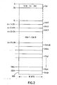
- FIG. 2 shows diagrammatically the organization of the memory map for the arrangement of Figure 1.
- This memory map MM is a random access memory (RAM) and contains a total of sixty-four chapters CH1 to CH64 each of which comprises lK16 words or 2K8 bytes, as aforesaid.
- the byte address of the 0 to 2K bytes of each chapter can be identified by a 10-bit address code which addresses the 1024 words, in conjunction with a further bit which identifies the odd or even byte of an addressed word.
- the sixty-four chapters CH1 to CH64 can themselves be identified by respective code combinations of a 6-bit address code which serves as a so-called "chapter pointer".
- Certain chapters CHpl to CHpn of the memory map serve as the display memory 7.
- Each such chapter can store the digital codes for one "page" of data display.
- Other chapters serve as the DRCS character memory 9.
- mode T DRCS characters are stored in the DRCS memory 9, so that 50 (51) such characters can be stored in each chapter; that is each character requires two words for its storage.
- an additional chapter CHda is also allocated to serve as part of the DRCS character memory 9.
- FIG. 3 the elements there shown for DRCS addressing are embodied in the logic and processor circuit 4 (Fig. 1).
- the memory map MM (which accommodates the display memory and the DRCS memory, as aforesaid) and the fixed character memory 8 are also shown.
- a display is to use DRCS characters (as previously transmitted from a remote data source and stored in the DRCS memory)
- this is detected by the circuit 4 from the attribute data stored in the display memory 7 and one of two DRCS chapter latches L1 and L2 is set.
- the latch Ll is set, a 6-bit address code is applied over an address bus AD1 as a chapter pointer to identify the additional DRCS chapter CHda of the memory map MM.
- a DRCS address logic element ADL receives display data read out from the display memory 7 over a 7-bit address bus CCD, this display data identifying the characters to be displayed.
- the logic element ADL also receives over a 4-bit address bus DRD a dot row address which identifies the particular one of the ten dot rows of a character that is to be displayed on the scanning line concerned.
- the logic element ADL is responsive to the received display data and dot row address to produce on a 10-bit address bus DA the word address for the word containing a particular dot row of a particular DRCS character in the DRCS chapter CHda.
- the information in this word is read out on a 16-bit data bus DD. Twelve bits of this information is dot information which is fed via a select element SE associated with the shift registers 10 (Fig. 1). The remaining four bits of this information is mode information which is fed to the logic element ADL. This mode information is used, for instance in the manner set forth in our co-pending United Kingdom patent application No. 8233114 (PHB 32930) to determine a second word address containing the remainder of the information for the character concerned. This latter information is fed via the select element SE to the shift registers 10 which now contain all the dot information (i.e. 4 bits per pixel) for the mode T character selected.
- the DRCS characters of each of the DRCS character sets which are stored in the DRCS chapters CHdl to CHd20 are available for display only in any character position of a particular sub-area or sub-areas of the total display area of the screen.
- each sub-area has the same number of character positions as there are DRCS characters in the set individually associated with that sub-area.
- Figure 4 illustrates diagrammatically the theoretical division of the total display area TDA into twenty sub-areas SA1 to SA20. As aforesaid, the total display area contains 25 character rows RO to R24 each having 40 character positions CPO to CP39. Each character row is made up to ten scanning lines SLO to SL9.
- the sub-areas SA1 to SA20 are formed from successive pairs of character position columns. Each sub-area therefore contains fifty character positions.
- Each of the DRCS chapters CHdl to CHd20 which contain 50(51) mode T DRCS characters, are identified only for a respective portion of each line scanning period by means of a second chapter pointer which is represented by a 6-bit address code on a second address bus AD2.
- a settable 6-bit counter COU provides this latter 6-bit address code.
- the latch L2 When "full-field" DRCS data display is to be effected, the latch L2 is latched to the first chapter address (x) for the DRCS chapters CHdl to CHd20 and this address is set into the counter COU and is loaded onto the address bus AD2 at the beginning of each line scanning period by a pulse LP which occurs at the line scanning frequency.
- a pulse LP which occurs at the line scanning frequency.
- the counter COU is stepped by a divide-by-two circuit DV which is fed with column pulses CP. These column pulses CP occur at the beginning of each character column position of the display to effectively identify the character positions along the character rows.
- the DRCS chapter CHdl is addressed for a portion of that period corresponding to the first two character column positions, and then the count of the counter COU is increased by one so that the second DRCS chapter CHd2 is addresed for a similar portion of the line scanning period corresponding to the next two character column positions, and so on, until the end of the scanning line period.
- the counter COU is reset to the original count position to identify the DRCS chapter CHdl again, and the sequential addressing of the DRCS chapters CHdl to CHd20 is repeated in the next line scanning period, and thereafter in each successive line scanning period of the complete raster scan.
- each DRCS character of a set stored in one of these chapters can be individually and uniquely associated with a respective character position in the sub-area concerned, which means that each character dot position of a DRCS character can be individually and uniquely associated with a respective pixel position of the character position concerned to provide a high resolution graphics display.
- the fixed character memory 8 which is addressed directly by the character code on bus CCD and dot row number on bus DRD from the display memory 7 to produce dot information for character display using characters from this memory 8.
- the display memory itself is addressed by character row addresses RO to R24 andcharacter column addresses CCO to CC39 to read out the character codes on the bus CCD for the successive characters of the display.
- the various pulses used in the arrangement of Figure 3 are produced by a pulse counting chain, shown diagramatically in Figure 5, which forms part of the timing circuit 15 (Fig. 1).
- This pulse counting chain comprises a number of counters 16 to 19 and is fed by dot pulses DP from a pulse generator 20, these dot pulses occurring at a bit frequency fd for the display.
- the first counter 16 is a modulo-12 column counter which produces a recurrent cycle of twelve dot pulses DPPO to DPP11 corresponding to the twelve dot positions of a character dot row. These pulses DPPO to DPP11 are used (in a manner not shown) to address for serial read-out from the shift registers (10-Fig.l) the successive dots of a character dot row for display.
- the counter 17, which receives a stepping pulse (column pulse CP) once per cycle of the counter 12. is. a modulo-40 character position counter that produces the forty character position addresses CRPO to CRP39.
- the counter 18, which receives a stepping pulse (line pulse LP) once per cycle of the counter 17, is a modulo-10 row counter that produces the dot row addresses DRO to DR9, and the counter 19, which receives a stepping pulse once per cycle of the counter 18, is a modulo-25 counter that produces the character row addresses RO to R24.
- each DRCS chapter contains sufficient characters for four character position columns of the display, so that the counter COU has to be stepped only once every fourth character position column, instead of once every second character position column, to provide the appropriate chapter pointer addresses.
- This change in the stepping rate can readily be effected by changing the divisor number of the divider circuit DV from 2 to 4.
- the chapter pointer addressing can be altered by modifying the physical connections of the address bus AD2 between the counter COU and the memory map MM.
- Figure 6 shows the normal one-to-one connection of each of the address bus connections of the bus AD2 between six output terminals OT1 to OT6 on the counter COU and six input terminals IT1 to IT6 on the memory map MM.
- Figure 7 shows the modified address bus connections of the bus AD2 for addressing only half the number of DRCS chapters, whilst maintaining a divisor of 2 for the divider circuit DV.
- a lesser number of DRCS chapters can be provided so that two (or more) sub-areas "share" the same DRCS chapters.
- the chapter addressing would be implemented as already described for a full-field DRCS display.
- the contents of the display memory 7 can assign DRCS characters of an addressed chapter to selected character positions in the sub-areas concerned, these positions corresponding to fine detail and having DRCS characters uniquely associated with them.
- Unfilled character positions of the sub-areas can be assigned characters from the fixed character memory 8 (usually spaces) or characters from the DRCS chapter memory CHdn which is available for the total display area.
Landscapes
- Engineering & Computer Science (AREA)
- Physics & Mathematics (AREA)
- Computer Hardware Design (AREA)
- General Physics & Mathematics (AREA)
- Theoretical Computer Science (AREA)
- Controls And Circuits For Display Device (AREA)
- Digital Computer Display Output (AREA)
Applications Claiming Priority (2)
| Application Number | Priority Date | Filing Date | Title |
|---|---|---|---|
| GB08405069A GB2155286B (en) | 1984-02-27 | 1984-02-27 | Character memory addressing for data display |
| GB8405069 | 1984-02-27 |
Publications (2)
| Publication Number | Publication Date |
|---|---|
| EP0153789A2 true EP0153789A2 (fr) | 1985-09-04 |
| EP0153789A3 EP0153789A3 (fr) | 1988-11-09 |
Family
ID=10557232
Family Applications (1)
| Application Number | Title | Priority Date | Filing Date |
|---|---|---|---|
| EP85200223A Withdrawn EP0153789A3 (fr) | 1984-02-27 | 1985-02-20 | Adressage de mémoires de caractères pour l'affichage de données |
Country Status (4)
| Country | Link |
|---|---|
| US (1) | US4672371A (fr) |
| EP (1) | EP0153789A3 (fr) |
| JP (1) | JPS60205486A (fr) |
| GB (1) | GB2155286B (fr) |
Cited By (2)
| Publication number | Priority date | Publication date | Assignee | Title |
|---|---|---|---|---|
| EP0272006A3 (fr) * | 1986-12-16 | 1989-10-18 | Ing. C. Olivetti & C., S.p.A. | Contrôleur de visualisation pour les appareils de traitement des données |
| EP0942406A1 (fr) * | 1998-03-10 | 1999-09-15 | Koninklijke Philips Electronics N.V. | Affichage point par point sur écran semi-graphique |
Families Citing this family (5)
| Publication number | Priority date | Publication date | Assignee | Title |
|---|---|---|---|---|
| US4806921A (en) * | 1985-10-04 | 1989-02-21 | Ateq Corporation | Rasterizer for pattern generator |
| US5317684A (en) * | 1986-02-17 | 1994-05-31 | U.S. Philips Corporation | Method of storing character data in a display device |
| US4937565A (en) * | 1986-06-24 | 1990-06-26 | Hercules Computer Technology | Character generator-based graphics apparatus |
| US5633656A (en) * | 1993-05-05 | 1997-05-27 | Acer Peripherals, Inc. | Controlling apparatus for display of an on-screen menu in a display device |
| US10353797B2 (en) * | 2006-12-29 | 2019-07-16 | International Business Machines Corporation | Using memory tracking data to inform a memory map tool |
Family Cites Families (5)
| Publication number | Priority date | Publication date | Assignee | Title |
|---|---|---|---|---|
| FR2382049A1 (fr) * | 1977-02-23 | 1978-09-22 | Thomson Csf | Processeur pour terminal informatique utilisant un recepteur de television |
| EP0024862A3 (fr) * | 1979-09-04 | 1981-03-25 | Harold Charles Taylor | Appareil vidéo de visualisation de plages juxtaposées de couleurs selectionnées |
| GB2059727B (en) * | 1979-09-27 | 1983-03-30 | Ibm | Digital data display system |
| JPS5799686A (en) * | 1980-12-11 | 1982-06-21 | Omron Tateisi Electronics Co | Display controller |
| US4439761A (en) * | 1981-05-19 | 1984-03-27 | Bell Telephone Laboratories, Incorporated | Terminal generation of dynamically redefinable character sets |
-
1984
- 1984-02-27 GB GB08405069A patent/GB2155286B/en not_active Expired
-
1985
- 1985-01-31 US US06/696,629 patent/US4672371A/en not_active Expired - Fee Related
- 1985-02-20 EP EP85200223A patent/EP0153789A3/fr not_active Withdrawn
- 1985-02-23 JP JP60033706A patent/JPS60205486A/ja active Granted
Cited By (3)
| Publication number | Priority date | Publication date | Assignee | Title |
|---|---|---|---|---|
| EP0272006A3 (fr) * | 1986-12-16 | 1989-10-18 | Ing. C. Olivetti & C., S.p.A. | Contrôleur de visualisation pour les appareils de traitement des données |
| EP0942406A1 (fr) * | 1998-03-10 | 1999-09-15 | Koninklijke Philips Electronics N.V. | Affichage point par point sur écran semi-graphique |
| FR2776109A1 (fr) * | 1998-03-10 | 1999-09-17 | Philips Electronics Nv | Affichage point par point sur ecran semi-graphique |
Also Published As
| Publication number | Publication date |
|---|---|
| GB8405069D0 (en) | 1984-04-04 |
| JPS60205486A (ja) | 1985-10-17 |
| US4672371A (en) | 1987-06-09 |
| EP0153789A3 (fr) | 1988-11-09 |
| GB2155286B (en) | 1987-04-23 |
| JPH0530279B2 (fr) | 1993-05-07 |
| GB2155286A (en) | 1985-09-18 |
Similar Documents
| Publication | Publication Date | Title |
|---|---|---|
| US4918434A (en) | T.V. game system | |
| US4823120A (en) | Enhanced video graphics controller | |
| EP0138244B1 (fr) | Dispositif d'affichage de caractères à taille variable comportant des caractères obscurcis | |
| CA1148285A (fr) | Dispositif d'affichage de trame | |
| US4814756A (en) | Video display control system having improved storage of alphanumeric and graphic display data | |
| US4139838A (en) | Color pattern and alphanumeric character generator for use with raster-scan display devices | |
| US4486856A (en) | Cache memory and control circuit | |
| US4408197A (en) | Pattern display apparatus | |
| EP0138243B1 (fr) | Algorithme de double hauteur pour l'affichage de caractères sur un dispositif à TRC | |
| EP0184246A2 (fr) | Générateur électronique de signaux couleur et système d'affichage d'images en couleur comportant ce générateur | |
| US3955189A (en) | Data display terminal having data storage and transfer apparatus employing matrix notation addressing | |
| US4766427A (en) | Display apparatus with display screen splitting function | |
| US4672371A (en) | Data display arrangements | |
| EP0004797A2 (fr) | Dispositif de commande d'un appareil d'affichage à balayage à trame | |
| EP0299582B1 (fr) | Décodeur de télétexte | |
| US4910687A (en) | Bit gating for efficient use of RAMs in variable plane displays | |
| JPS60140294A (ja) | ビツトマツピング型ビデオ表示装置 | |
| US4695835A (en) | Data display systems | |
| US4390780A (en) | LSI Timing circuit for a digital display employing a modulo eight counter | |
| EP0194404B1 (fr) | Compteur à double but pour le rafraîchissement de l'écran et la mémoire | |
| KR950008023B1 (ko) | 래스터 주사 표시 시스템 | |
| US4742347A (en) | Refreshing circuit for multi-panel display | |
| EP0136748A2 (fr) | Dispositif d'affichage de données avec décalage lisse | |
| CA1191635A (fr) | Circuit de chronometrage pour afficheur numerique utilisant un compteur modulo huit | |
| GB2245461A (en) | Accented character generator |
Legal Events
| Date | Code | Title | Description |
|---|---|---|---|
| PUAI | Public reference made under article 153(3) epc to a published international application that has entered the european phase |
Free format text: ORIGINAL CODE: 0009012 |
|
| AK | Designated contracting states |
Designated state(s): DE FR GB IT SE |
|
| RAP3 | Party data changed (applicant data changed or rights of an application transferred) |
Owner name: N.V. PHILIPS' GLOEILAMPENFABRIEKEN Owner name: PHILIPS ELECTRONIC AND ASSOCIATED INDUSTRIES LIMIT |
|
| PUAL | Search report despatched |
Free format text: ORIGINAL CODE: 0009013 |
|
| AK | Designated contracting states |
Kind code of ref document: A3 Designated state(s): DE FR GB IT SE |
|
| 17P | Request for examination filed |
Effective date: 19890428 |
|
| STAA | Information on the status of an ep patent application or granted ep patent |
Free format text: STATUS: THE APPLICATION HAS BEEN WITHDRAWN |
|
| 18W | Application withdrawn |
Withdrawal date: 19911102 |
|
| R18W | Application withdrawn (corrected) |
Effective date: 19911102 |
|
| RIN1 | Information on inventor provided before grant (corrected) |
Inventor name: BUGG, RICHARD EDWARD FREDERICK |