EP0154556A2 - Procédé de fabrication d'un dispositif d'affichage à cristal liquide en couleur du type à matrice - Google Patents
Procédé de fabrication d'un dispositif d'affichage à cristal liquide en couleur du type à matrice Download PDFInfo
- Publication number
- EP0154556A2 EP0154556A2 EP85301577A EP85301577A EP0154556A2 EP 0154556 A2 EP0154556 A2 EP 0154556A2 EP 85301577 A EP85301577 A EP 85301577A EP 85301577 A EP85301577 A EP 85301577A EP 0154556 A2 EP0154556 A2 EP 0154556A2
- Authority
- EP
- European Patent Office
- Prior art keywords
- active matrix
- voltage
- matrix substrate
- electrodeposited
- display electrode
- Prior art date
- Legal status (The legal status is an assumption and is not a legal conclusion. Google has not performed a legal analysis and makes no representation as to the accuracy of the status listed.)
- Granted
Links
Images


Classifications
-
- G—PHYSICS
- G02—OPTICS
- G02F—OPTICAL DEVICES OR ARRANGEMENTS FOR THE CONTROL OF LIGHT BY MODIFICATION OF THE OPTICAL PROPERTIES OF THE MEDIA OF THE ELEMENTS INVOLVED THEREIN; NON-LINEAR OPTICS; FREQUENCY-CHANGING OF LIGHT; OPTICAL LOGIC ELEMENTS; OPTICAL ANALOGUE/DIGITAL CONVERTERS
- G02F1/00—Devices or arrangements for the control of the intensity, colour, phase, polarisation or direction of light arriving from an independent light source, e.g. switching, gating or modulating; Non-linear optics
- G02F1/01—Devices or arrangements for the control of the intensity, colour, phase, polarisation or direction of light arriving from an independent light source, e.g. switching, gating or modulating; Non-linear optics for the control of the intensity, phase, polarisation or colour
- G02F1/13—Devices or arrangements for the control of the intensity, colour, phase, polarisation or direction of light arriving from an independent light source, e.g. switching, gating or modulating; Non-linear optics for the control of the intensity, phase, polarisation or colour based on liquid crystals, e.g. single liquid crystal display cells
- G02F1/133—Constructional arrangements; Operation of liquid crystal cells; Circuit arrangements
- G02F1/1333—Constructional arrangements; Manufacturing methods
- G02F1/1335—Structural association of cells with optical devices, e.g. polarisers or reflectors
- G02F1/133509—Filters, e.g. light shielding masks
- G02F1/133514—Colour filters
- G02F1/133516—Methods for their manufacture, e.g. printing, electro-deposition or photolithography
-
- Y—GENERAL TAGGING OF NEW TECHNOLOGICAL DEVELOPMENTS; GENERAL TAGGING OF CROSS-SECTIONAL TECHNOLOGIES SPANNING OVER SEVERAL SECTIONS OF THE IPC; TECHNICAL SUBJECTS COVERED BY FORMER USPC CROSS-REFERENCE ART COLLECTIONS [XRACs] AND DIGESTS
- Y10—TECHNICAL SUBJECTS COVERED BY FORMER USPC
- Y10S—TECHNICAL SUBJECTS COVERED BY FORMER USPC CROSS-REFERENCE ART COLLECTIONS [XRACs] AND DIGESTS
- Y10S359/00—Optical: systems and elements
- Y10S359/90—Methods
Definitions
- This invention relates to a method of manufacturing liquid crystal display devices and in particular to a method of manufacturing a color-matrix-type liquid crystal display device having self-aligned color filters formed on an active matrix substrate.
- a matrix-type liquid crystal display (LCD) device comprises a matrix substrate having a plurality of display electrodes, a counter substrate spaced from the matrix substrate, and liquid crystal filling the space between the two substrates.
- Color filters in a conventional matrix-type LCD, are arranged in the counter substrate, i.e., they are manufactured independently from the matrix substrate before assembly of the display device.
- An electrodeposition method for manufacturing stripe-type color filters is described in M. Suginoya et al.
- a method of manufacturing a colour liquid crystal display device having a plurality of picture element units each including a display electrode comprising: immersing the device in a dye containing liquid, and applying to one or more of the display electrodes a voltage of sufficient value and for sufficient time to form an electrodeposited filter layer on the display electrode.
- a method of forming a filter on an active matrix substrate for a colour-matrix-type liquid crystal display device comprising a plurality of picture element units arranged on a substrate in a matrix of rows and columns, each picture element unit including a switching element and a display electrode
- the method comprising the steps of: immersing the active matrix substrate into an emulsion comprising colouring matter of a predetermined colour; applying a voltage to at least one selected display electrode, the voltage being of a value, and applied for a length of time, sufficient to form an electrodeposited filter layer of the predetermined colour on the display electrode; removing the active matrix substrate from the emulsion; and _.curing the electrodeposited filter layer.
- a colour-matrix-type LCD is manufactured having an active matrix substrate, that is, a substrate in which it is possible individually to switch each coloured dot of the dot matrix.
- each picture element unit includes a switching element and a display electrode.
- the switching element were activated only during a displaying operation. The invention, however, utilises them also during the manufacturing process.
- the active matrix substrate is immersed, as one electrode into an emulsion containing colouring matter for electrodeposition. Then voltages are supplied to selected display electrodes by controlling the corresponding switching elements so as to form electrodeposited filter layers directly onto the selected display electrodes. After removing the active matrix substrate from the emulsion, it is cured. These steps are repeated for each colour (red, green, blue).
- self-aligned colour filters can be obtained, without colour misalignment, and irrespective of the size of the matrix or the size of each individual display electrode.
- the density (thickness) of the colour filters may be controlled simply by controlling the voltages being supplied to the display electrodes. This makes it possible to vary the densities of colour filters within a single LCD to compensate for differences in the amount of light passing through different display electrodes. Also, dot-matrix colour filters can be easily manufactured by this electrodeposition process regardless of the colours.
- FIG. 1 shows an equivalent circuit diagram of an active matrix substrate used in a preferred embodiment according to this invention.
- the active matrix substrate includes a plurality of unit display pixels arranged in an n x m matrix.
- Each unit display pixel in the preferred embodiment, consists of three contiguous picture element units in a single row of the matrix.
- Each picture element unit includes a switching element of, for example, an N-channel enhancement MOSFET, a capacitor for storing a display drive voltage, and a transparent display electrode made, for example, of ITO (Indium-Tin-Oxide).
- the picture element unit in the upper-left corner in Figure 1, for example, has a transistor 1, capacitor 2 and display electrode 3.
- successive electrodes 3, 4, 5 form one unit display pixel.
- a unit display pixel may be formed, for example, by electrodes 3, 4 and 20.
- at least one display electrode of each unit display pixel must be colored in one of the selected colors (red, blue and green, in the preferred embodiment) by the method described below.
- Each picture element unit in a row of the matrix is connected to a common address line.
- Each picture element unit in a column of the matrix is connected to a common data line.
- the gates of all transistors in the first row of the matrix are connected to address line 9, and the gates of all transistors in the second row are connected to address line 10.
- the drains of all transistors in the first and second columns of the matrix are connected, respectively, to data lines 13 and 14.
- a color image will be displayed as follows.
- An address drive circuit 8 supplies a high level voltage successively to each address line 9, 10, ... 11.
- a data drive circuit 12 supplies an entire row of data, of the color image being displayed, to data lines 13, 14, 15, 16 ..., in response to the selection of address lines by address drive circuit 8.
- the first address line 9 is driven high, the first-row data of the color image is supplied to all data lines.
- the high level voltage on address line 9 causes each transistor in the first row in the matrix to conduct, so that the first-row data is stored in the capacitors of the first row of the matrix.
- the voltage of each capacitor will be used for controlling the amount of red, blue and green light passing through the liquid crystal so as to display a coloured dot image.
- FIG. 2 shows a vertical sectional view of the active matrix substrate indicating a unit display pixel located in the i-th row and j-th column of the matrix.
- Each picture element unit has the same configuration formed on a transparent glass substrate 30.
- a gate electrode 31 constituting the gate of the transistor and an ITO electrode 32 constituting one plate of the capacitor are formed on the glass substrate 30.
- An Si0 2 film 33 is formed by chemical vapor deposition (CVD) on gate electrode 31 and ITO electrode 32, serving as both the gate insulator and the capacitor dielectric.
- Display electrode 34 also made of transparent ITO, is formed on film 33 directly over ITO electrode 32 so as to serve as the other plate of the capacitor.
- Amorphous silicon layer 35 is also deposited on film 33, directly over gate electrode 31.
- Drain electrode 36 and source electrode 37 are formed on amorphous silicon layer 35 to complete the switching transistor.
- Part of source electrode 37 is formed on display electrode 34 in order to connect the two electrically.
- a passivation film 38 which insulates various electrodes is provided over the entire surface except for the major portion of display electrode 34.
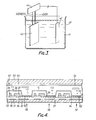
- FIG. 3 shows an electrodeposition apparatus which may be used to form color filters on the display electrodes of the above active matrix substrate, in the preferred embodiment of the invention.
- An electrodeposition tub 40 is filled with electrodeposition emulsion 41 which is a mixed emulsion containing a solution of polyester-melamine resin and a non-water-soluble dye dispersed in water.
- the above active matrix substrate as one electrode 43, is immersed in the emulsion 41.
- Electrode 43 is the one which is to be subjected to electrodeposition.
- a counter electrode 42 consisting of stainless steel, is immersed so as to face the display electrodes of the active matrix substrate. Both electrodes 42 and 43 are coupled to a DC voltage source of, for example, 15 V through a switching circuit 44.
- Switching circuit 44 which functions as both address drive circuit 8 and data drive circuit 12, selects address lines and data lines of the active matrix substrate to designate display electrodes on which color filters or electrodeposited layers should be formed. It is preferable for electrode 43 to have a higher potential relative to counter electrode 42 when using an anionic dye as a coloring matter.
- suitable dyes are Perylene (trade name) for red and Cu-Phthalocyanimes (trade name) for green and blue (manufactured by Sumitomo Kagaku Co.).
- red filter layers are electrodeposited on display electrodes R ll , ⁇ ,R lm , ⁇ ,R nm of active matrix substrate 43.
- active matrix substrate 43 is immersed in electrodeposition tub 40 filled with an emulsion containing a solution of polyester-melmine resin and Perylene (trade name) dispersed in water
- switching circuit 44 supplies predetermined voltages to address lines and data lines as shown in the first row of Table 1, to select display electrodes R ll , ⁇ ,R lm ⁇ ,R nm ⁇
- switching circuit 44 supplies 15 V selectively to data lines D R1 , D R2 , ⁇ ,D Rm .
- the remaining data lines are kept at O V.
- the thickness of red coloring matter deposited on the selected display electrodes depends on the voltage being applied to the selected display electrodes, so that about 1 um of thickness was given by the above voltages.
- the active matrix substrate is removed from the tub and cured at a temperature of about 453 K for 30 minutes so as to affix the red coloring matter to the selected display electrodes.
- green filter layers are electrodeposited on display elec- trodes G ll , ⁇ ,G lm , ⁇ ,G nm of active matrix substrate 43.
- switching circuit 44 supplies DC voltages to address lines and data lines as shown in the second row of Table 1, to select display electrodes G ll , ⁇ G lm , ⁇ ,G nm .
- the active matrix substrate is removed from the emulsion and cured so as to affix the green coloring matter to the selected display electrodes.
- blue filter layers are similarly electrodeposited onto display electrodes B ll , ⁇ ,B lm , ⁇ ,B nm of active matrix substrate 43 by supplying voltages shown in the third row of Table 1, and then the substrate is cured.
- red electrodeposited layer 50, green electrodeposited layer 51 and blue electrodeposited layer 52 are formed on the active matrix substrate, on selected display electrodes 34.
- an orientating layer 54 is formed over layers 50, 51 and 52 and the passivation film.
- an orientating electrode 55 and another orientating layer 56 are provided on a glass substrate 53 spaced from and facing the active matrix substrate.
- the intervening space is filled with liquid crystal 57 as a display medium. Since the resulting LCD is of the transparent type, it is illuminated from the back of the active matrix substrate with white backlight 58 including red, green and blue light components.
- the hue and brightness of transmitted light are controlled by the transmissivity of liquid crystal 57, which is determined by the voltage applied to the display electrodes 34.
- a color active matrix liquid crystal display device can be manufactured, irrespective of the size of the screen, or the size of the display electrodes, by producing the color by a method in which only those display electrodes which are to be colored are selected using the matrix drive and then the coloring matter is electrodeposited onto these display electrodes.
- This enables a self aligned color filter to be produced without risk of color misalignment, since the display electrodes themselves provide the colored surface.
- a color liquid crystal display device of high recognizability or visual quality can be manufactured. It should be noted that the same effect can be obtained even using non-linear devices as the switching elements, and the technique can also be applied to active matrix substrates using metal for the display electrodes in the absence of capacitors.
- each electrodeposited filter has substantially the same thickness.
- the amount of light passing through all filters is the same.
- This assumption is, however, not always justified, for example, such as when a long, narrow fluorescent lamp is used as a backlight source.
- the light distribution from the fluorescent lamp usually diminishes toward the edge of the array.
- some display electrodes which are located near the edges of the active matrix substrate receive less light than those which are located near the center portion of the active matrix substrate.
- FIG. 5 is a flowchart showing a process for forming electrodeposited filters on an active matrix substrate, similar to the previous embodiment of this invention.
- the light distribution (from the backlight which will be used for illuminating the color LCD) is measured (step Sl).
- the appropriate thickness for each filter is determined in step S2, so as to compensate for variations in the amount of light.
- the calculation results in a value for the applied voltage for each display electrode, since the applied voltage mainly defines the thickness of ⁇ the filter layer to be formed by electrodeposition. For example, when 10 V is applied to the display electrode, the thickness of the filter layer is about 0.8 um, while it is about 2.3 um with an applied voltage of 30 V.
- the calculated voltage for peripheral display electrodes will be lower than the voltage for centrally located display electrodes, in order to get substantially the same illumination through each.
- steps S3 through S8 are basically similar to the first embodiment of the invention.
- red filter layers are formed by electrodeposition, and then the active matrix is cured in step S4.
- green filter layers are formed by electrodeposition in step S5 followed by curing in step S6.
- blue filter layers are formed by electrodeposition in step S7 and cured in step S8.
- steps S3, 55 and S7 are slightly different from the first embodiment in order to form filter layers having different thicknesses. As in the first embodiment, however, each color of filter is electrodeposited in all applicable rows of the matrix before the next color is deposited.
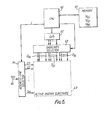
- FIG. 6 is a block diagram showing a circuit which supplies necessary voltages to address lines and data lines of the active matrix substrate in step S3 of Figure 5.
- the circuit includes CPU 60 for controlling the entire circuit, memory 61 for storing control programs by which CPU 60 is operated and also voltage data calculated for step S3 of Figure 5, digital to analog converter 62, data line selector 63 and address line selector 64.
- FIG. 7 is a flowchart indicating the operation of CPU 60 in Figure 6 for forming red filter layers.
- CPU 60 supplies the content of the inner counter to address line selector 64.
- Address line selector 64 supplies predetermined voltage (15 V) provided from terminal 65 to one of address lines Gj which is designated by the inner counter in step S12.
- CPU 60 reads a set of voltage data Y Rj1 ,Y Rj2 , ⁇ ,Y Rjm from memory 61, the voltages which should be applied to the display electrodes R j1 ,R j2 , ⁇ ,R jm located in the j-th row of the matrix.
- step S14 of Figure 7 CPU 60 waits for a time sufficient to complete the electro- position on each selected display electrode. Then the inner counter is incremented by 1 in step S15, and the content is compared with a value N in step S16.
- steps S12 through S16 are repeated for the next row of the matrix.
- the content of the inner counter is greater than N, that is, after every row of the matrix has been selected, the active matrix substrate 43 is removed from the tub.
- Steps S5 through S7 of Figure 5 are similarly executed except that data line selector 63 selects data lines D Gi and D B i, respectively, and corresponding voltage data V Gji and V B ji stored in memory 61 are used.
- the manufactured color active matrix LCD has a self- compensation for the light distribution of back light.
Landscapes
- Physics & Mathematics (AREA)
- Nonlinear Science (AREA)
- Engineering & Computer Science (AREA)
- Manufacturing & Machinery (AREA)
- Mathematical Physics (AREA)
- Chemical & Material Sciences (AREA)
- Crystallography & Structural Chemistry (AREA)
- General Physics & Mathematics (AREA)
- Optics & Photonics (AREA)
- Liquid Crystal (AREA)
- Optical Filters (AREA)
Applications Claiming Priority (2)
| Application Number | Priority Date | Filing Date | Title |
|---|---|---|---|
| JP59042930A JPS60188927A (ja) | 1984-03-08 | 1984-03-08 | カラ−・マトリツクス型液晶表示装置の製造方法 |
| JP42930/84 | 1984-03-08 |
Publications (3)
| Publication Number | Publication Date |
|---|---|
| EP0154556A2 true EP0154556A2 (fr) | 1985-09-11 |
| EP0154556A3 EP0154556A3 (en) | 1987-06-16 |
| EP0154556B1 EP0154556B1 (fr) | 1991-08-07 |
Family
ID=12649729
Family Applications (1)
| Application Number | Title | Priority Date | Filing Date |
|---|---|---|---|
| EP85301577A Expired EP0154556B1 (fr) | 1984-03-08 | 1985-03-07 | Procédé de fabrication d'un dispositif d'affichage à cristal liquide en couleur du type à matrice |
Country Status (4)
| Country | Link |
|---|---|
| US (1) | US4709990A (fr) |
| EP (1) | EP0154556B1 (fr) |
| JP (1) | JPS60188927A (fr) |
| DE (1) | DE3583690D1 (fr) |
Cited By (3)
| Publication number | Priority date | Publication date | Assignee | Title |
|---|---|---|---|---|
| FR2625827A1 (fr) * | 1988-01-11 | 1989-07-13 | Commissariat Energie Atomique | Ecran d'affichage en couleur a matrice active sans croisement des conducteurs lignes d'adressage et des conducteurs colonnes de commande |
| EP0431249A3 (en) * | 1989-12-08 | 1992-05-13 | International Business Machines Corporation | Electrostatic deposition of lcd color filters |
| EP0636932A1 (fr) * | 1993-07-26 | 1995-02-01 | Shinto Paint Co., Ltd. | Méthode pour fabriquer un substrat portant des films en forme de cadre et fenêtre sur sa surface |
Families Citing this family (8)
| Publication number | Priority date | Publication date | Assignee | Title |
|---|---|---|---|---|
| US5191452A (en) * | 1989-09-20 | 1993-03-02 | Honeywell Inc. | Active matrix liquid crystal display fabrication for grayscale |
| KR920005444B1 (ko) * | 1989-12-02 | 1992-07-04 | 삼성전자 주식회사 | 칼라필터 및 그 제조방법 |
| US5843332A (en) * | 1991-10-21 | 1998-12-01 | Dai Nippon Printing Co., Ltd. | Polymer dispersion-type liquid crystal optical device and method for producing the same |
| DE69228789T2 (de) * | 1991-11-21 | 1999-07-22 | Fujitsu Ltd., Kawasaki, Kanagawa | Farbige Flüssigkristall-Anzeigevorrichtung |
| CA2132618A1 (fr) * | 1992-04-09 | 1993-10-10 | Raychem Corporation | Methode d'electrodeposition de cristaux liquides encapsules sur des electrodes |
| EP0659282B1 (fr) * | 1992-09-11 | 1998-11-25 | Kopin Corporation | Systeme de filtre colore pour ecran de visualisation |
| WO2002067054A2 (fr) * | 2001-02-21 | 2002-08-29 | International Business Machines Corporation | Structuration de photoresist haute resolution sur les structures a multiples couches deposees sur des substrats |
| US7411589B2 (en) * | 2004-04-30 | 2008-08-12 | Honeywell International Inc. | Liquid crystal color display system and method |
Family Cites Families (6)
| Publication number | Priority date | Publication date | Assignee | Title |
|---|---|---|---|---|
| NL111927C (fr) * | 1956-06-14 | |||
| US3681223A (en) * | 1970-07-27 | 1972-08-01 | Corning Glass Works | Electrophoretic deposition of color phosphors |
| GB2122794B (en) * | 1982-06-15 | 1985-09-18 | Standard Telephones Cables Ltd | Liquid crystal display |
| JPS5990818A (ja) * | 1982-11-16 | 1984-05-25 | Seiko Epson Corp | カラ−フイルタ−の製造方法 |
| US4522691A (en) * | 1982-12-22 | 1985-06-11 | Seiko Instruments & Electronics Ltd. | Method for manufacturing a multicolor filter and a multicolor display device |
| JPS6023834A (ja) * | 1983-07-19 | 1985-02-06 | Seiko Instr & Electronics Ltd | マトリクス型多色表示装置用基板の製造方法 |
-
1984
- 1984-03-08 JP JP59042930A patent/JPS60188927A/ja active Pending
-
1985
- 1985-03-07 EP EP85301577A patent/EP0154556B1/fr not_active Expired
- 1985-03-07 DE DE8585301577T patent/DE3583690D1/de not_active Expired - Lifetime
- 1985-03-08 US US06/709,666 patent/US4709990A/en not_active Expired - Lifetime
Cited By (4)
| Publication number | Priority date | Publication date | Assignee | Title |
|---|---|---|---|---|
| FR2625827A1 (fr) * | 1988-01-11 | 1989-07-13 | Commissariat Energie Atomique | Ecran d'affichage en couleur a matrice active sans croisement des conducteurs lignes d'adressage et des conducteurs colonnes de commande |
| EP0431249A3 (en) * | 1989-12-08 | 1992-05-13 | International Business Machines Corporation | Electrostatic deposition of lcd color filters |
| EP0636932A1 (fr) * | 1993-07-26 | 1995-02-01 | Shinto Paint Co., Ltd. | Méthode pour fabriquer un substrat portant des films en forme de cadre et fenêtre sur sa surface |
| US5503732A (en) * | 1993-07-26 | 1996-04-02 | Shinto Paint Co., Ltd. | Method for manufacturing a substrate having window-shaped and frame-shaped coating films on the surface thereof |
Also Published As
| Publication number | Publication date |
|---|---|
| DE3583690D1 (de) | 1991-09-12 |
| JPS60188927A (ja) | 1985-09-26 |
| EP0154556A3 (en) | 1987-06-16 |
| US4709990A (en) | 1987-12-01 |
| EP0154556B1 (fr) | 1991-08-07 |
Similar Documents
| Publication | Publication Date | Title |
|---|---|---|
| US4653862A (en) | Liquid crystal display device having color filters sized to prevent light leakage between pixels | |
| US4773737A (en) | Color display panel | |
| EP0721603B1 (fr) | Disposition de pixels pour ecran plat | |
| KR100259783B1 (ko) | 다수의 컬러 개별 레벨 디스플레이를 위한 디스플레이 픽셀 밸런싱 | |
| US5311205A (en) | Color liquid-crystal display apparatus with rectilinear arrangement | |
| US5317437A (en) | Display apparatus with pixels having subpixel regions | |
| EP0167408B1 (fr) | Circuit de commande pour un dispositif d'affichage en couleurs à cristaux liquides | |
| EP0154556B1 (fr) | Procédé de fabrication d'un dispositif d'affichage à cristal liquide en couleur du type à matrice | |
| JPH0296118A (ja) | 液晶表示装置 | |
| KR100544070B1 (ko) | 액티브매트릭스 액정표시소자를 이용한 필드·순차형액정표시장치 | |
| JPS5910988A (ja) | カラ−液晶表示器 | |
| JPWO2000020918A1 (ja) | 液晶装置および電子機器 | |
| JPH02282785A (ja) | カラーディスプレイ装置 | |
| DE69938037T2 (de) | Flüssigkristallanzeige mit aktiver matrix | |
| JPS6385525A (ja) | 強誘電性液晶カラ−電気光学装置 | |
| EP0096856B1 (fr) | Affichage à cristal liquide | |
| JPH0422498B2 (fr) | ||
| JPS63189841A (ja) | 液晶表示装置の製造方法 | |
| US5341151A (en) | Liquid crystal colour display device with zig-zag pattern | |
| JPH0454207B2 (fr) | ||
| US5748268A (en) | Quasi-tiled active matrix display | |
| JP2007529771A (ja) | カラーディスプレイデバイス及びその製造方法 | |
| KR101429907B1 (ko) | 액정 표시장치 | |
| JPH10239710A (ja) | 液晶表示装置 | |
| JPH0688967A (ja) | 液晶表示装置 |
Legal Events
| Date | Code | Title | Description |
|---|---|---|---|
| PUAI | Public reference made under article 153(3) epc to a published international application that has entered the european phase |
Free format text: ORIGINAL CODE: 0009012 |
|
| 17P | Request for examination filed |
Effective date: 19850322 |
|
| AK | Designated contracting states |
Designated state(s): DE FR GB NL |
|
| PUAL | Search report despatched |
Free format text: ORIGINAL CODE: 0009013 |
|
| AK | Designated contracting states |
Kind code of ref document: A3 Designated state(s): DE FR GB NL |
|
| 17Q | First examination report despatched |
Effective date: 19890704 |
|
| GRAA | (expected) grant |
Free format text: ORIGINAL CODE: 0009210 |
|
| AK | Designated contracting states |
Kind code of ref document: B1 Designated state(s): DE FR GB NL |
|
| PG25 | Lapsed in a contracting state [announced via postgrant information from national office to epo] |
Ref country code: NL Effective date: 19910807 |
|
| REF | Corresponds to: |
Ref document number: 3583690 Country of ref document: DE Date of ref document: 19910912 |
|
| ET | Fr: translation filed | ||
| NLV1 | Nl: lapsed or annulled due to failure to fulfill the requirements of art. 29p and 29m of the patents act | ||
| PLBE | No opposition filed within time limit |
Free format text: ORIGINAL CODE: 0009261 |
|
| STAA | Information on the status of an ep patent application or granted ep patent |
Free format text: STATUS: NO OPPOSITION FILED WITHIN TIME LIMIT |
|
| 26N | No opposition filed | ||
| REG | Reference to a national code |
Ref country code: GB Ref legal event code: 746 Effective date: 19981008 |
|
| REG | Reference to a national code |
Ref country code: FR Ref legal event code: D6 |
|
| REG | Reference to a national code |
Ref country code: GB Ref legal event code: IF02 |
|
| PGFP | Annual fee paid to national office [announced via postgrant information from national office to epo] |
Ref country code: GB Payment date: 20040303 Year of fee payment: 20 |
|
| PGFP | Annual fee paid to national office [announced via postgrant information from national office to epo] |
Ref country code: FR Payment date: 20040309 Year of fee payment: 20 |
|
| PGFP | Annual fee paid to national office [announced via postgrant information from national office to epo] |
Ref country code: DE Payment date: 20040318 Year of fee payment: 20 |
|
| PG25 | Lapsed in a contracting state [announced via postgrant information from national office to epo] |
Ref country code: GB Free format text: LAPSE BECAUSE OF EXPIRATION OF PROTECTION Effective date: 20050306 |
|
| REG | Reference to a national code |
Ref country code: GB Ref legal event code: PE20 |