EP0154774A2 - Transmission de données avec bus de données bidirectionnel - Google Patents
Transmission de données avec bus de données bidirectionnel Download PDFInfo
- Publication number
- EP0154774A2 EP0154774A2 EP85100534A EP85100534A EP0154774A2 EP 0154774 A2 EP0154774 A2 EP 0154774A2 EP 85100534 A EP85100534 A EP 85100534A EP 85100534 A EP85100534 A EP 85100534A EP 0154774 A2 EP0154774 A2 EP 0154774A2
- Authority
- EP
- European Patent Office
- Prior art keywords
- data
- control unit
- peripheral
- addressed
- data bus
- Prior art date
- Legal status (The legal status is an assumption and is not a legal conclusion. Google has not performed a legal analysis and makes no representation as to the accuracy of the status listed.)
- Granted
Links
Images

Classifications
-
- G—PHYSICS
- G06—COMPUTING OR CALCULATING; COUNTING
- G06F—ELECTRIC DIGITAL DATA PROCESSING
- G06F13/00—Interconnection of, or transfer of information or other signals between, memories, input/output devices or central processing units
- G06F13/38—Information transfer, e.g. on bus
- G06F13/42—Bus transfer protocol, e.g. handshake; Synchronisation
- G06F13/4204—Bus transfer protocol, e.g. handshake; Synchronisation on a parallel bus
- G06F13/4208—Bus transfer protocol, e.g. handshake; Synchronisation on a parallel bus being a system bus, e.g. VME bus, Futurebus, Multibus
- G06F13/4217—Bus transfer protocol, e.g. handshake; Synchronisation on a parallel bus being a system bus, e.g. VME bus, Futurebus, Multibus with synchronous protocol
-
- H—ELECTRICITY
- H04—ELECTRIC COMMUNICATION TECHNIQUE
- H04Q—SELECTING
- H04Q9/00—Arrangements in telecontrol or telemetry systems for selectively calling a substation from a main station, in which substation desired apparatus is selected for applying a control signal thereto or for obtaining measured values therefrom
- H04Q9/14—Calling by using pulses
- H04Q9/16—Calling by using pulses by predetermined number of pulses
Definitions
- the invention is based on a data transmission between a control unit and via a clock line, an enable line and a data line connected to these individually addressable peripheral components for executing the commands issued by the control unit and for reporting data back to the control unit via a bidirectional data bus, the The peripheral blocks are addressed using the different word lengths of the data.
- control unit e.g. a microprocessor
- peripheral components connected to them in the form of integrated circuits for executing the commands issued by the control unit
- the control unit often requests feedback from the circuits addressed by it, so that the data flow on the data line must be possible in both directions.
- An arrangement in which a plurality of integrated circuits which can be addressed by a microprocessor are supplied with data via a data line.
- This is a system with a constant word length for addressing, data transmission and for the command to report data in the opposite direction. Due to the constant word length e.g. 8 bits in an 8 bit system result in very long commands, which take a corresponding amount of time to transmit. So you need e.g. for addressing, for the data and for the command for feedback, 8 bits each. The unnecessarily large word length is particularly disadvantageous for the last-mentioned command, since 8 bits must be transmitted due to the system, although a single bit would suffice.
- a data transmission system is also known in which the word length is variable and the peripheral modules are addressed using the word length determined.
- no bidirectional data bus is provided in this data transmission system.
- the object of the invention is to enable bidirectional data transmission between a control unit and a plurality of peripheral components connected to it, without providing a special command for this on the data line.
- the invention has the advantage that the data transmission is particularly fast since the time for the transmission of a special command is saved because the command is derived from the control signals of the control unit.
- the object on which the invention is based is achieved by the invention disclosed in the patent claim. Further advantageous possibilities for applying the invention result from the subclaims.
- the microprocessor 1 shows the control unit, for example a microprocessor, which corresponds to peripheral components 2, 3, 4 and 5.
- the microprocessor 1 has a connection labeled DATA, via which data can be sent to the peripheral components 2 to 5 and received by them via the bidirectional data line.
- the EN output activates the individual components 2 to 5 and synchronously with the clock signal CL the data is transferred.
- Each block 2 to 5 has a counter 8 or 9.
- the blocks are addressed in that a signal for accepting the data is sent via the EN input which is at H potential after the data has been input and which coincides with the counter output at H potential is derived in the corresponding module.
- the outputs Z1, Zn deliver signals after a different number of clock pulses CL. In this way, depending on the word length of the data, different modules can be addressed.
- the data stored in the catch register 6, 7 are at the inputs of the working memories 16 and 17 (latch) which, depending on the coincidence of the output signals of the counters 8 and 9, take over the data with the EN signal and put them at the outputs.
- the EN signal with L potential occurs, all counters are reset.
- a bistable flip-flop shown here as RS flip-flop 12 or 13 is set via the AND circuit 10 or 11, the output signals of which activate the response memory 14 or 15, which occurs when it arrives of clock pulses CL outputs the data to the control unit 1.
- the flip-flop 12 or 13 is reset again and the data flow from the response register 14 or 15 is prevented.
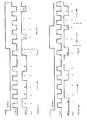
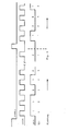
- FIG. 2 shows the case in which data from the control unit 1 are present at the data inputs of the peripheral modules 2 to 5. After the nth clock pulse there is an n-bit word in the catch registers of blocks 2 to 5. Block n, whose counter is set to the value n, takes the data into its working memory.
- the block to be addressed is determined using the positive edge of the EN signal. Immediately after this edge, the bits of the response to the data line 18 reach the control unit 1 in synchronism with the clock signal.
Landscapes
- Engineering & Computer Science (AREA)
- Theoretical Computer Science (AREA)
- Computer Networks & Wireless Communication (AREA)
- Physics & Mathematics (AREA)
- General Engineering & Computer Science (AREA)
- General Physics & Mathematics (AREA)
- Communication Control (AREA)
- Information Transfer Systems (AREA)
- Small-Scale Networks (AREA)
- Computer And Data Communications (AREA)
- Bus Control (AREA)
- Bidirectional Digital Transmission (AREA)
Priority Applications (1)
| Application Number | Priority Date | Filing Date | Title |
|---|---|---|---|
| AT85100534T ATE77724T1 (de) | 1984-02-10 | 1985-01-19 | Datenuebertragung mit bidirektionalem datenbus. |
Applications Claiming Priority (2)
| Application Number | Priority Date | Filing Date | Title |
|---|---|---|---|
| DE3404721A DE3404721C2 (de) | 1984-02-10 | 1984-02-10 | Schaltungsanordnung zur Übertragung von Daten |
| DE3404721 | 1984-02-10 |
Publications (3)
| Publication Number | Publication Date |
|---|---|
| EP0154774A2 true EP0154774A2 (fr) | 1985-09-18 |
| EP0154774A3 EP0154774A3 (en) | 1988-10-05 |
| EP0154774B1 EP0154774B1 (fr) | 1992-06-24 |
Family
ID=6227325
Family Applications (1)
| Application Number | Title | Priority Date | Filing Date |
|---|---|---|---|
| EP85100534A Expired - Lifetime EP0154774B1 (fr) | 1984-02-10 | 1985-01-19 | Transmission de données avec bus de données bidirectionnel |
Country Status (5)
| Country | Link |
|---|---|
| EP (1) | EP0154774B1 (fr) |
| JP (1) | JPH06100997B2 (fr) |
| AT (1) | ATE77724T1 (fr) |
| DE (2) | DE3404721C2 (fr) |
| HK (1) | HK15396A (fr) |
Cited By (1)
| Publication number | Priority date | Publication date | Assignee | Title |
|---|---|---|---|---|
| EP0434083A3 (en) * | 1989-12-21 | 1992-03-04 | Kabushiki Kaisha Toshiba | Data transfer system and method of transferring data |
Families Citing this family (1)
| Publication number | Priority date | Publication date | Assignee | Title |
|---|---|---|---|---|
| DE3829454A1 (de) * | 1988-08-31 | 1990-03-01 | Thomson Brandt Gmbh | Serielle datenschnittstelle |
Family Cites Families (1)
| Publication number | Priority date | Publication date | Assignee | Title |
|---|---|---|---|---|
| GB1221964A (en) * | 1967-04-18 | 1971-02-10 | Ibm | Data transmission system |
-
1984
- 1984-02-10 DE DE3404721A patent/DE3404721C2/de not_active Expired - Lifetime
-
1985
- 1985-01-19 AT AT85100534T patent/ATE77724T1/de not_active IP Right Cessation
- 1985-01-19 EP EP85100534A patent/EP0154774B1/fr not_active Expired - Lifetime
- 1985-01-19 DE DE8585100534T patent/DE3586252D1/de not_active Expired - Fee Related
- 1985-02-08 JP JP60022071A patent/JPH06100997B2/ja not_active Expired - Lifetime
-
1996
- 1996-01-25 HK HK15396A patent/HK15396A/xx not_active IP Right Cessation
Cited By (1)
| Publication number | Priority date | Publication date | Assignee | Title |
|---|---|---|---|---|
| EP0434083A3 (en) * | 1989-12-21 | 1992-03-04 | Kabushiki Kaisha Toshiba | Data transfer system and method of transferring data |
Also Published As
| Publication number | Publication date |
|---|---|
| EP0154774B1 (fr) | 1992-06-24 |
| JPS60209864A (ja) | 1985-10-22 |
| DE3404721A1 (de) | 1985-08-14 |
| DE3586252D1 (de) | 1992-07-30 |
| EP0154774A3 (en) | 1988-10-05 |
| ATE77724T1 (de) | 1992-07-15 |
| JPH06100997B2 (ja) | 1994-12-12 |
| DE3404721C2 (de) | 1991-07-25 |
| HK15396A (en) | 1996-02-02 |
Similar Documents
| Publication | Publication Date | Title |
|---|---|---|
| DE2457553C2 (de) | Asynchrone Taktgebereinrichtung | |
| DE3300260C2 (fr) | ||
| DE3300261C2 (fr) | ||
| DE2157982A1 (de) | Digitales Multiprozessor-Datenverarbeitungssystem | |
| DE3418248A1 (de) | Datenverarbeitungsanlage mit einer anordnung zur datenuebertragung zwischen einem speicher und einem zentralen prozessor | |
| DE1424762B2 (de) | Datenverarbeitungsanlage | |
| DE2406740A1 (de) | System zur regelung von verfahrensausruestungen | |
| EP0006164A1 (fr) | Système multiprocesseur avec mémoires utilisables en commun | |
| DE3508321A1 (de) | Programmierbare schaltung zur steuerung einer fluessigkristallanzeige | |
| DE3501194C2 (de) | Verfahren und Vorrichtung zum Datenaustausch zwischen Mikroprozessoren | |
| DE2905676A1 (de) | Integrierte schaltung mit einem einzigen chip | |
| DE4005042A1 (de) | Architektur eines digitalen bewegungssteuerungselements hoher geschwindigkeit | |
| DE3042105C2 (fr) | ||
| DE2154488A1 (de) | Datenübertragungs-Unterkanal einer Datenverarbeitungsanlage | |
| EP0154774B1 (fr) | Transmission de données avec bus de données bidirectionnel | |
| DE68924876T2 (de) | Integrierte Halbleiterschaltungen. | |
| EP0065272B1 (fr) | Système multiprocesseur | |
| EP0356873B1 (fr) | Interface de données sériel | |
| EP0301160A2 (fr) | Système à deux microprocesseurs et mémoire écriture/lecture partagée | |
| DE19948598B4 (de) | Mikrocomputer mit Abtastfunktion eines Wiederholungs-Anforderungssignals in Synchronisation mit einem Abtastsignal | |
| DE3248276C2 (fr) | ||
| DE3826266C2 (fr) | ||
| DE3104928C2 (de) | Multi-Mikrorechneranlage mit direktem Speicherzugriff | |
| DE3214576C2 (de) | Schaltungsanordnung zum Ermitteln von Dauerlagesignalen auf Anschlußleitungen einer Vermittlungsanlage | |
| DE2756764C3 (de) | Einrichtung zur Synchronisation von Prozessor und Speicher in einer elektronischen Datenverarbeitungsanlage |
Legal Events
| Date | Code | Title | Description |
|---|---|---|---|
| PUAI | Public reference made under article 153(3) epc to a published international application that has entered the european phase |
Free format text: ORIGINAL CODE: 0009012 |
|
| AK | Designated contracting states |
Designated state(s): AT CH DE FR GB IT LI NL SE |
|
| PUAL | Search report despatched |
Free format text: ORIGINAL CODE: 0009013 |
|
| AK | Designated contracting states |
Kind code of ref document: A3 Designated state(s): AT CH DE FR GB IT LI NL SE |
|
| 17P | Request for examination filed |
Effective date: 19890313 |
|
| 17Q | First examination report despatched |
Effective date: 19910219 |
|
| GRAA | (expected) grant |
Free format text: ORIGINAL CODE: 0009210 |
|
| AK | Designated contracting states |
Kind code of ref document: B1 Designated state(s): AT CH DE FR GB IT LI NL SE |
|
| REF | Corresponds to: |
Ref document number: 77724 Country of ref document: AT Date of ref document: 19920715 Kind code of ref document: T |
|
| ITF | It: translation for a ep patent filed | ||
| GBT | Gb: translation of ep patent filed (gb section 77(6)(a)/1977) | ||
| REF | Corresponds to: |
Ref document number: 3586252 Country of ref document: DE Date of ref document: 19920730 |
|
| ET | Fr: translation filed | ||
| ET1 | Fr: translation filed ** revision of the translation of the patent or the claims | ||
| PLBE | No opposition filed within time limit |
Free format text: ORIGINAL CODE: 0009261 |
|
| STAA | Information on the status of an ep patent application or granted ep patent |
Free format text: STATUS: NO OPPOSITION FILED WITHIN TIME LIMIT |
|
| 26N | No opposition filed | ||
| EAL | Se: european patent in force in sweden |
Ref document number: 85100534.8 |
|
| PGFP | Annual fee paid to national office [announced via postgrant information from national office to epo] |
Ref country code: GB Payment date: 19960105 Year of fee payment: 12 |
|
| PGFP | Annual fee paid to national office [announced via postgrant information from national office to epo] |
Ref country code: FR Payment date: 19960115 Year of fee payment: 12 |
|
| PGFP | Annual fee paid to national office [announced via postgrant information from national office to epo] |
Ref country code: SE Payment date: 19960126 Year of fee payment: 12 Ref country code: AT Payment date: 19960126 Year of fee payment: 12 |
|
| PGFP | Annual fee paid to national office [announced via postgrant information from national office to epo] |
Ref country code: NL Payment date: 19960129 Year of fee payment: 12 |
|
| PGFP | Annual fee paid to national office [announced via postgrant information from national office to epo] |
Ref country code: CH Payment date: 19960206 Year of fee payment: 12 |
|
| PGFP | Annual fee paid to national office [announced via postgrant information from national office to epo] |
Ref country code: DE Payment date: 19960316 Year of fee payment: 12 |
|
| PG25 | Lapsed in a contracting state [announced via postgrant information from national office to epo] |
Ref country code: GB Effective date: 19970119 Ref country code: AT Effective date: 19970119 |
|
| PG25 | Lapsed in a contracting state [announced via postgrant information from national office to epo] |
Ref country code: SE Effective date: 19970120 |
|
| PG25 | Lapsed in a contracting state [announced via postgrant information from national office to epo] |
Ref country code: LI Effective date: 19970131 Ref country code: CH Effective date: 19970131 |
|
| PG25 | Lapsed in a contracting state [announced via postgrant information from national office to epo] |
Ref country code: NL Effective date: 19970801 |
|
| GBPC | Gb: european patent ceased through non-payment of renewal fee |
Effective date: 19970119 |
|
| REG | Reference to a national code |
Ref country code: CH Ref legal event code: PL |
|
| PG25 | Lapsed in a contracting state [announced via postgrant information from national office to epo] |
Ref country code: FR Effective date: 19970930 |
|
| NLV4 | Nl: lapsed or anulled due to non-payment of the annual fee |
Effective date: 19970801 |
|
| PG25 | Lapsed in a contracting state [announced via postgrant information from national office to epo] |
Ref country code: DE Effective date: 19971001 |
|
| EUG | Se: european patent has lapsed |
Ref document number: 85100534.8 |
|
| REG | Reference to a national code |
Ref country code: FR Ref legal event code: ST |