EP0155008A2 - Filtre numérique pour la séparation de signaux en sous-bandes - Google Patents
Filtre numérique pour la séparation de signaux en sous-bandes Download PDFInfo
- Publication number
- EP0155008A2 EP0155008A2 EP85103027A EP85103027A EP0155008A2 EP 0155008 A2 EP0155008 A2 EP 0155008A2 EP 85103027 A EP85103027 A EP 85103027A EP 85103027 A EP85103027 A EP 85103027A EP 0155008 A2 EP0155008 A2 EP 0155008A2
- Authority
- EP
- European Patent Office
- Prior art keywords
- wave digital
- digital filter
- signals
- sampling rate
- filters
- Prior art date
- Legal status (The legal status is an assumption and is not a legal conclusion. Google has not performed a legal analysis and makes no representation as to the accuracy of the status listed.)
- Granted
Links
Images


Classifications
-
- H—ELECTRICITY
- H03—ELECTRONIC CIRCUITRY
- H03H—IMPEDANCE NETWORKS, e.g. RESONANT CIRCUITS; RESONATORS
- H03H17/00—Networks using digital techniques
- H03H17/02—Frequency selective networks
- H03H17/0201—Wave digital filters
Definitions
- the invention relates to a digital filter arrangement according to the preamble of patent claim 1.
- the source signal is broken down into subbands using a filter bank. These subbands are transmitted in coded form, e.g. ADPCM, and decoded at the location of the sink and reconstructed in another filter bank. It is a so-called subband coding, for which the term "subband coding" has also become established in English. Details on this can be found, for example, in the magazine BSTJ 1981, pages 1633 to 1653. Transversal (FIR) filters are used there to implement the filter banks. However, it turns out that secondary conditions (quadrature - mirror filters) to be met for distortion-free transmission are only approximately met.
- FIR Transversal
- the invention has for its object to significantly reduce the technical complexity of these known circuits and to ensure a distortion-free transmission; circuits are therefore specified using digital wave filters with which these conditions can be met.
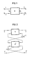
- a wave digital filter N is shown again for better understanding, the inputs of which are designated 1 and 2 and the input signals A 1 and A 2 occur there accordingly.
- the output signals B 1 and B2 appear at the connections 1 'and 2', the gate resistors R 1 and R 2 are indicated between the gates. Details of such wave digital filters can be found, for example, in the literature references in the accompanying bibliography, in particular in AEÜ 25, 79-89, 1971.
- two wave digital filters are connected, namely a wave digital filter N and a wave digital filter N T.
- the input lines 1 and 2 and the output lines 1 'and 2' can again be seen.
- the outputs of the wave digital filter N are now, so to speak, fed to the inputs of the wave digital filter N T , with a sign inverter (-1) I being connected in one of the connecting lines.
- These lines now lead to the inputs of the wave digital filter N T and its outputs are connected to the outputs 1 'and 2' of the overall circuit.
- the one output of the wave digital filter N T in the exemplary embodiment the output leading to the output line 2 ', in turn contains a sign inverter (-1) I.
- the wave digital filter N can and must be described by a scattering matrix S. then the wave digital filter N T have the scattering matrix S T.
- the input signals are denoted by a 1 and a 2 and the output signals by b 1 and b 2 .
- the further details are functional details which also refer directly to FIG. 1 and which will be discussed later.
- the circuit of FIG. 3 is practically identical to that of FIG. 2, but the multipliers u (n) and v (n) are also connected to the wave digital filter N T. To indicate this, the input signals are designated c 1 and c 2 there .
- FIG. 4 A possible modification is shown in FIG. 4, where it can be seen that the output signals b 1 and b 2 are connected together via inverters (-1) n and a subsequent summer to form the output signal d (nT).
- the individual circuit paths are connected to one another via the adders marked “plus”, delay elements of delay time T or 2T are also provided, and finally the multipliers already mentioned ( ⁇ 1 , ⁇ 2 , ⁇ 3 ) are also included.
- the input paths LP and HP can also be seen, and the combination at the output takes place via a multiplier with the coefficient 0.5.
- Some of the adders can also be replaced by subtractors, as indicated by the minus sign.
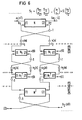
- FIG. 6 shows a wave digital filter N, which is followed by two further wave digital filters N1.
- the combination of the output signals b 1 and b 2 also takes place here to a certain extent via a “cross-connection” for the signal b 2 via a sign inverter “-1”.
- Multipliers u (n) and v (n) are connected to the other connecting lines, at which signals c 1 and c 2 then occur.
- the signals c 1 and c 2 are fed to the first inputs of the wave digital filter N 1 , the second input of which receives no input signal (0).
- An inverter (-1) then follows again in one of the output lines and multipliers u 1 (n), v 1 (n) then follow.
- the transmission circuit is now complete.
- the signals must now be assembled in the opposite order using the transposed wave digital filters N 1 T or N. This happens to a certain extent in the opposite order, each with the connection of inverters "-1", but without the use of multipliers, and the output signal b 2 (nT) is then present at one output of the transposed wave digital filter N.
- FIG. 7 An interpolating filter circuit is shown in FIG. 7, the inputs being labeled 1A, 2A, 3A and 4A.
- the exit . is marked with E.
- this is also a possible overall circuit in which corresponding further multipliers are then also required.
- These multipliers are designated g 1 to g 5 there , the individual functions can be found directly in the associated circuit diagram. Only further delay elements with the delay time 4T have to be used, which can also be found in the circuit.
- a wave digital filter (WDF) two-port has two input and two output connections. If this is used appropriately and a wave digital filter is connected to its transposed wave digital filter, the filter effect is completely compensated for, with the exception of an all-pass phase, and this is independent of selectivity requirements. This point of view also applies if every second sample at the connection points is reduced to zero, provided that a certain condition, which is easy to meet, is fulfilled. Very effective solutions are then possible.
- the method is of particular interest, for example, for subband coding.
- WVDFs wave digital filters
- WVDFs wave digital filters
- connections gates each of which consists of an input and an output connection 1.2 J.
- a conventional filter represents a two-port, so to speak
- a conventional wave digital filter has two input terminals and two output terminals.
- the filter have complementary transmission characteristics [3 to 6]
- the following figures show how some other interesting characteristics can be obtained by connecting two or more wave digital filters together, making use of the fact that each of these wave digital filters does more than just has one connection and more than one output.
- the design process can be repeated as often as required.
- the method can be used to achieve an exact solution to the problem for so-called quadrature mirror filters according to references [9] to [12], which are used in subband coding circuits [10, 11, 13 (subband coding)].
- N T can be derived from N by using flow reversal [14]. Specifically, the values of the multiplier coefficients in N D are then the same as in N, that is, for a given N, the corresponding N T can be obtained without approximation.
- S and S T It can therefore be shown that Equation 4 also applies in which As already explained in FIG. 2, the left side of equation (4) can be regarded as the scatter matrix of the overall circuit shown there. For this arrangement, the transfer function from the connections 1 to 2 'and from the connections 1' to 2 are thus zero and thus from the connections 1 to 1 'and from 2 to 3' are both det S.
- equation (2) the transfer function from the connections 1 to 2 'and from the connections 1' to 2 are thus zero and thus from the connections 1 to 1 'and from 2 to 3' are both det S.
- the circuit of FIG. 3 differs from the circuit of FIG. 2 in that the additional multipliers u (n) and v (n) are switched on. to halve the sampling rate in the special embodiment of FIG. 3.
- the functions u (n) and v (n) alternately assume the values 1 and zero and are thus either in phase or in opposite phase. This can be represented according to equations (8) and (9). It is also applies and thus the following values result for the signals c 1 and c 2
- Equation 15 holds the output signal at the output terminal 1 'contains no other frequency components than the input signal. This result is also retained, regardless of the design of the wave digital filter N, and even if this wave digital filter, for example, only fulfills very low separation requirements for the original signal in individual frequency bands, regardless of the fact that every second sample value is set to zero by the use the multipliers u (n) and v (n). The reconstructed signal is therefore available in inverted or non-inverted form at one of the outputs 2 'or 1'.
- the output signals b 1 (nT) and b 2 (nT) of the circuit of FIG. 3 are combined to form a new output signal d (nT) in the adder identified there by "+".
- the output signal b 2 runs via a sign inverter (-1) n .
- the value of the output signal d (nT) can thus be doubled.
- the above can be used directly for the circuit shown in FIG. 6.
- the crossover output signals c 1 and c 2 which are reduced in their sampling rate, are frequency-divided via further wave digital filters N 1 and, in turn, their sampling rate is reduced.
- the multipliers u 1 , v 1 must accordingly be provided there.
- these signals are processed further via the transposed wave digital filter N 1 T and combined in the output-side wave digital filter N T , so that the output signal b 2 (nT) can be taken there after the inverter (-1).
- the dimensioning method specified here has the advantage that an exact amplitude reproduction of the spectrum of the original signal is achieved even if the coefficients are rounded in an arbitrary manner.
Landscapes
- Physics & Mathematics (AREA)
- Engineering & Computer Science (AREA)
- Computer Hardware Design (AREA)
- Mathematical Physics (AREA)
- Compression, Expansion, Code Conversion, And Decoders (AREA)
- Complex Calculations (AREA)
- Transmission Systems Not Characterized By The Medium Used For Transmission (AREA)
- Dc Digital Transmission (AREA)
- Reduction Or Emphasis Of Bandwidth Of Signals (AREA)
Priority Applications (1)
| Application Number | Priority Date | Filing Date | Title |
|---|---|---|---|
| AT85103027T ATE70674T1 (de) | 1984-03-16 | 1985-03-15 | Digitale filteranordnung zur aufteilung von signalen in teilbaender. |
Applications Claiming Priority (2)
| Application Number | Priority Date | Filing Date | Title |
|---|---|---|---|
| DE3409817 | 1984-03-16 | ||
| DE3409817 | 1984-03-16 |
Publications (3)
| Publication Number | Publication Date |
|---|---|
| EP0155008A2 true EP0155008A2 (fr) | 1985-09-18 |
| EP0155008A3 EP0155008A3 (en) | 1987-06-03 |
| EP0155008B1 EP0155008B1 (fr) | 1991-12-18 |
Family
ID=6230789
Family Applications (1)
| Application Number | Title | Priority Date | Filing Date |
|---|---|---|---|
| EP85103027A Expired - Lifetime EP0155008B1 (fr) | 1984-03-16 | 1985-03-15 | Filtre numérique pour la séparation de signaux en sous-bandes |
Country Status (3)
| Country | Link |
|---|---|
| EP (1) | EP0155008B1 (fr) |
| AT (1) | ATE70674T1 (fr) |
| DE (1) | DE3584901D1 (fr) |
Cited By (3)
| Publication number | Priority date | Publication date | Assignee | Title |
|---|---|---|---|---|
| DE3627679A1 (de) * | 1986-08-14 | 1988-02-25 | Blaupunkt Werke Gmbh | Filteranordnung |
| GB2258963A (en) * | 1991-08-23 | 1993-02-24 | Sony Broadcast & Communication | Sub-band filters |
| EP0501690A3 (en) * | 1991-02-28 | 1993-07-21 | British Aerospace Public Limited Company | Apparatus for and method of digital signal processing |
Family Cites Families (1)
| Publication number | Priority date | Publication date | Assignee | Title |
|---|---|---|---|---|
| DE3314647A1 (de) * | 1983-04-22 | 1984-10-25 | Siemens AG, 1000 Berlin und 8000 München | Wellendigitalfilter unter verwendung von brueckenwellendigitalfiltern |
-
1985
- 1985-03-15 EP EP85103027A patent/EP0155008B1/fr not_active Expired - Lifetime
- 1985-03-15 AT AT85103027T patent/ATE70674T1/de active
- 1985-03-15 DE DE8585103027T patent/DE3584901D1/de not_active Expired - Lifetime
Cited By (5)
| Publication number | Priority date | Publication date | Assignee | Title |
|---|---|---|---|---|
| DE3627679A1 (de) * | 1986-08-14 | 1988-02-25 | Blaupunkt Werke Gmbh | Filteranordnung |
| EP0501690A3 (en) * | 1991-02-28 | 1993-07-21 | British Aerospace Public Limited Company | Apparatus for and method of digital signal processing |
| GB2258963A (en) * | 1991-08-23 | 1993-02-24 | Sony Broadcast & Communication | Sub-band filters |
| US5268905A (en) * | 1991-08-23 | 1993-12-07 | Sony United Kingdom Limited | Sub band filters |
| GB2258963B (en) * | 1991-08-23 | 1995-06-14 | Sony Broadcast & Communication | Sub band filters |
Also Published As
| Publication number | Publication date |
|---|---|
| EP0155008A3 (en) | 1987-06-03 |
| EP0155008B1 (fr) | 1991-12-18 |
| DE3584901D1 (de) | 1992-01-30 |
| ATE70674T1 (de) | 1992-01-15 |
Similar Documents
| Publication | Publication Date | Title |
|---|---|---|
| EP0290790B1 (fr) | Banc de filtres | |
| DE2626122C2 (de) | Anordnung zum Verarbeiten von Signalen in einem Frequenzmultiplex-Übertragungssystem | |
| DE2831059C2 (de) | Integrierender Kodeumsetzer | |
| DE3705209C2 (fr) | ||
| DE3621737C2 (fr) | ||
| EP0155008B1 (fr) | Filtre numérique pour la séparation de signaux en sous-bandes | |
| EP0256286B1 (fr) | Dispositif de filtrage | |
| DE3922469C2 (fr) | ||
| EP0397912B1 (fr) | Méthode et montage pour obtenir le gradient des signaux de sortie d'un réseau donné pour traiter des signaux à temps discret en fonction des paramètres du circuit | |
| DE2011772C3 (de) | Filter mit einer periodischen Frequenzcharakteristik | |
| EP0075311B1 (fr) | Dispositif pour la transmission de la parole utilisant le principe des vocodeurs à canaux | |
| DE3883414T2 (de) | Digitales Signalverarbeitungssystem mit einer Filterbank. | |
| DE3705206C2 (fr) | ||
| DE3836081C1 (en) | Filter bank for frequency multiplexing or frequency demultiplexing of channel signals | |
| EP0339037B1 (fr) | Filtre de demi-bande non recurrent | |
| EP0258574A2 (fr) | Dispositif de filtrage | |
| DE1912674A1 (de) | Digitaler Phasen-Entzerrer | |
| EP0065648B1 (fr) | Procédé de permutation en fréquence de bandes partielles | |
| DE3047450A1 (de) | "filter zur aenderung der abtastfrequenz" | |
| DE19627784C1 (de) | Digitale Filterweiche | |
| EP0367932A2 (fr) | Bancs de filtres pour le multiplexage/démultiplexage en fréquence de signaux de canaux | |
| DE3318228C2 (fr) | ||
| DE1902057C3 (de) | Verfahren und Schaltungsanordnung zur Ausfilterung eines Restseitenbandsignals aus einem Zweiseitenbandsignal | |
| EP0643483A1 (fr) | Banc de filtrage numérique | |
| DE3303132A1 (de) | Digitaler phasenlinearer tiefpass |
Legal Events
| Date | Code | Title | Description |
|---|---|---|---|
| PUAI | Public reference made under article 153(3) epc to a published international application that has entered the european phase |
Free format text: ORIGINAL CODE: 0009012 |
|
| AK | Designated contracting states |
Designated state(s): AT BE CH DE FR GB IT LI NL SE |
|
| PUAL | Search report despatched |
Free format text: ORIGINAL CODE: 0009013 |
|
| AK | Designated contracting states |
Kind code of ref document: A3 Designated state(s): AT BE CH DE FR GB IT LI NL SE |
|
| 17P | Request for examination filed |
Effective date: 19871106 |
|
| 17Q | First examination report despatched |
Effective date: 19900420 |
|
| GRAA | (expected) grant |
Free format text: ORIGINAL CODE: 0009210 |
|
| AK | Designated contracting states |
Kind code of ref document: B1 Designated state(s): AT BE CH DE FR GB IT LI NL SE |
|
| PG25 | Lapsed in a contracting state [announced via postgrant information from national office to epo] |
Ref country code: SE Effective date: 19911218 Ref country code: NL Effective date: 19911218 Ref country code: GB Effective date: 19911218 |
|
| REF | Corresponds to: |
Ref document number: 70674 Country of ref document: AT Date of ref document: 19920115 Kind code of ref document: T |
|
| REF | Corresponds to: |
Ref document number: 3584901 Country of ref document: DE Date of ref document: 19920130 |
|
| ET | Fr: translation filed | ||
| ITF | It: translation for a ep patent filed | ||
| NLV1 | Nl: lapsed or annulled due to failure to fulfill the requirements of art. 29p and 29m of the patents act | ||
| GBV | Gb: ep patent (uk) treated as always having been void in accordance with gb section 77(7)/1977 [no translation filed] | ||
| PLBE | No opposition filed within time limit |
Free format text: ORIGINAL CODE: 0009261 |
|
| STAA | Information on the status of an ep patent application or granted ep patent |
Free format text: STATUS: NO OPPOSITION FILED WITHIN TIME LIMIT |
|
| 26N | No opposition filed | ||
| PGFP | Annual fee paid to national office [announced via postgrant information from national office to epo] |
Ref country code: AT Payment date: 19960223 Year of fee payment: 12 |
|
| PGFP | Annual fee paid to national office [announced via postgrant information from national office to epo] |
Ref country code: BE Payment date: 19960319 Year of fee payment: 12 |
|
| PGFP | Annual fee paid to national office [announced via postgrant information from national office to epo] |
Ref country code: FR Payment date: 19960328 Year of fee payment: 12 |
|
| PGFP | Annual fee paid to national office [announced via postgrant information from national office to epo] |
Ref country code: DE Payment date: 19960520 Year of fee payment: 12 |
|
| PGFP | Annual fee paid to national office [announced via postgrant information from national office to epo] |
Ref country code: CH Payment date: 19960624 Year of fee payment: 12 |
|
| PG25 | Lapsed in a contracting state [announced via postgrant information from national office to epo] |
Ref country code: AT Effective date: 19970315 |
|
| PG25 | Lapsed in a contracting state [announced via postgrant information from national office to epo] |
Ref country code: LI Effective date: 19970331 Ref country code: CH Effective date: 19970331 Ref country code: BE Effective date: 19970331 |
|
| BERE | Be: lapsed |
Owner name: SIEMENS A.G. Effective date: 19970331 |
|
| REG | Reference to a national code |
Ref country code: CH Ref legal event code: PL |
|
| PG25 | Lapsed in a contracting state [announced via postgrant information from national office to epo] |
Ref country code: FR Free format text: LAPSE BECAUSE OF NON-PAYMENT OF DUE FEES Effective date: 19971128 |
|
| PG25 | Lapsed in a contracting state [announced via postgrant information from national office to epo] |
Ref country code: DE Effective date: 19971202 |
|
| REG | Reference to a national code |
Ref country code: FR Ref legal event code: ST |