EP0155117B1 - Dispositif pour détecter une tension - Google Patents
Dispositif pour détecter une tension Download PDFInfo
- Publication number
- EP0155117B1 EP0155117B1 EP85301327A EP85301327A EP0155117B1 EP 0155117 B1 EP0155117 B1 EP 0155117B1 EP 85301327 A EP85301327 A EP 85301327A EP 85301327 A EP85301327 A EP 85301327A EP 0155117 B1 EP0155117 B1 EP 0155117B1
- Authority
- EP
- European Patent Office
- Prior art keywords
- voltage
- layer
- capacitor
- polycrystalline silicon
- silicon dioxide
- Prior art date
- Legal status (The legal status is an assumption and is not a legal conclusion. Google has not performed a legal analysis and makes no representation as to the accuracy of the status listed.)
- Expired - Lifetime
Links
Images


Classifications
-
- G—PHYSICS
- G01—MEASURING; TESTING
- G01R—MEASURING ELECTRIC VARIABLES; MEASURING MAGNETIC VARIABLES
- G01R27/00—Arrangements for measuring resistance, reactance, impedance, or electric characteristics derived therefrom
-
- H—ELECTRICITY
- H03—ELECTRONIC CIRCUITRY
- H03K—PULSE TECHNIQUE
- H03K17/00—Electronic switching or gating, i.e. not by contact-making and –breaking
- H03K17/22—Modifications for ensuring a predetermined initial state when the supply voltage has been applied
-
- G—PHYSICS
- G01—MEASURING; TESTING
- G01R—MEASURING ELECTRIC VARIABLES; MEASURING MAGNETIC VARIABLES
- G01R19/00—Arrangements for measuring currents or voltages or for indicating presence or sign thereof
- G01R19/165—Indicating that current or voltage is either above or below a predetermined value or within or outside a predetermined range of values
- G01R19/16504—Indicating that current or voltage is either above or below a predetermined value or within or outside a predetermined range of values characterised by the components employed
- G01R19/16519—Indicating that current or voltage is either above or below a predetermined value or within or outside a predetermined range of values characterised by the components employed using FET's
Definitions
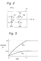
- a voltage detecting device for monitoring the magnitude of an input voltage, including voltage dividing circuitry comprising first and second capacitors, each of the type employing an oxide layer as the capacitor's dielectric, which capacitors are connected in series with one another, through a common node, between a reference voltage line and an input point to which the said input voltage is applied when the device is in use, and also including voltage detecting means, connected to the said common node, for generating an output signal when the potential at the said common node reaches a predetermined value, characterised in that the voltage detecting device further includes switching means arranged and connected so as to provide a conductive connection between the said common node and the reference voltage line when such monitoring is not required.
- Output data is transmitted from the Y-gates 6 via a sense amplifier 7 and an output data buffer 8 to an output terminal DO, while input data is supplied from an input terminal DI via an input data buffer/ latch circuit 9, a write/erase control circuit 10, and a charge pump circuit 11 to the Y-gates 6.
Landscapes
- Physics & Mathematics (AREA)
- General Physics & Mathematics (AREA)
- Read Only Memory (AREA)
- Non-Volatile Memory (AREA)
- Semiconductor Memories (AREA)
- Measurement Of Current Or Voltage (AREA)
Claims (7)
Applications Claiming Priority (2)
| Application Number | Priority Date | Filing Date | Title |
|---|---|---|---|
| JP35115/84 | 1984-02-28 | ||
| JP59035115A JPS60179998A (ja) | 1984-02-28 | 1984-02-28 | 電圧検出回路 |
Publications (3)
| Publication Number | Publication Date |
|---|---|
| EP0155117A2 EP0155117A2 (fr) | 1985-09-18 |
| EP0155117A3 EP0155117A3 (en) | 1986-12-10 |
| EP0155117B1 true EP0155117B1 (fr) | 1990-08-29 |
Family
ID=12432927
Family Applications (1)
| Application Number | Title | Priority Date | Filing Date |
|---|---|---|---|
| EP85301327A Expired - Lifetime EP0155117B1 (fr) | 1984-02-28 | 1985-02-27 | Dispositif pour détecter une tension |
Country Status (5)
| Country | Link |
|---|---|
| US (1) | US4636658A (fr) |
| EP (1) | EP0155117B1 (fr) |
| JP (1) | JPS60179998A (fr) |
| KR (1) | KR890004304B1 (fr) |
| DE (1) | DE3579333D1 (fr) |
Families Citing this family (11)
| Publication number | Priority date | Publication date | Assignee | Title |
|---|---|---|---|---|
| DE8714849U1 (de) * | 1986-12-23 | 1987-12-23 | Jenoptik Jena Gmbh, Ddr 6900 Jena | Geregelter CMOS-Substratspannungsgenerator |
| NL8800287A (nl) * | 1988-02-08 | 1989-09-01 | Philips Nv | Geheugenschakeling met een uitwisbaar programmeerbaar geheugen, generator voor het opwekken van een programmeerspanning voor het geheugen, spanningsregelaar en flankregelaar, beide geschikt voor toepassing in de generator, en een diode-element. |
| JP3124781B2 (ja) * | 1990-03-30 | 2001-01-15 | 富士通株式会社 | 半導体集積回路装置 |
| GB9320246D0 (en) * | 1993-10-01 | 1993-11-17 | Sgs Thomson Microelectronics | A driver circuit |
| KR100384854B1 (ko) * | 1997-03-21 | 2003-08-06 | 기아자동차주식회사 | 가변댐퍼의회전각측정장치 |
| US5874854A (en) * | 1997-03-28 | 1999-02-23 | International Business Machines Corporation | Control scheme for on-chip capacitor degating |
| US6204723B1 (en) * | 1999-04-29 | 2001-03-20 | International Business Machines Corporation | Bias circuit for series connected decoupling capacitors |
| US6518814B1 (en) * | 1999-12-28 | 2003-02-11 | Koninklijke Philips Electronics N.V. | High-voltage capacitor voltage divider circuit having a high-voltage silicon-on-insulation (SOI) capacitor |
| US6407898B1 (en) * | 2000-01-18 | 2002-06-18 | Taiwan Semiconductor Manufacturing Company Ltd. | Protection means for preventing power-on sequence induced latch-up |
| US7061308B2 (en) * | 2003-10-01 | 2006-06-13 | International Business Machines Corporation | Voltage divider for integrated circuits |
| WO2006052233A1 (fr) * | 2004-11-04 | 2006-05-18 | International Business Machines Corporation | Reducteur de tension pour des circuits integres |
Family Cites Families (8)
| Publication number | Priority date | Publication date | Assignee | Title |
|---|---|---|---|---|
| GB1357515A (en) * | 1972-03-10 | 1974-06-26 | Matsushita Electronics Corp | Method for manufacturing an mos integrated circuit |
| US3893146A (en) * | 1973-12-26 | 1975-07-01 | Teletype Corp | Semiconductor capacitor structure and memory cell, and method of making |
| CH615277A5 (en) * | 1976-08-31 | 1980-01-15 | Hitachi Ltd | Circuit arrangement for voltage detection |
| JPS55149871A (en) * | 1978-07-31 | 1980-11-21 | Fujitsu Ltd | Line voltage detector |
| US4451748A (en) * | 1982-01-15 | 1984-05-29 | Intel Corporation | MOS High voltage switching circuit |
| US4521696A (en) * | 1982-07-06 | 1985-06-04 | Motorola, Inc. | Voltage detecting circuit |
| US4543594A (en) * | 1982-09-07 | 1985-09-24 | Intel Corporation | Fusible link employing capacitor structure |
| US4527180A (en) * | 1983-01-31 | 1985-07-02 | Intel Corporation | MOS Voltage divider structure suitable for higher potential feedback regulation |
-
1984
- 1984-02-28 JP JP59035115A patent/JPS60179998A/ja active Granted
-
1985
- 1985-02-25 US US06/704,995 patent/US4636658A/en not_active Expired - Lifetime
- 1985-02-26 KR KR1019850001191A patent/KR890004304B1/ko not_active Expired
- 1985-02-27 EP EP85301327A patent/EP0155117B1/fr not_active Expired - Lifetime
- 1985-02-27 DE DE8585301327T patent/DE3579333D1/de not_active Expired - Lifetime
Also Published As
| Publication number | Publication date |
|---|---|
| EP0155117A3 (en) | 1986-12-10 |
| JPS60179998A (ja) | 1985-09-13 |
| KR890004304B1 (ko) | 1989-10-30 |
| EP0155117A2 (fr) | 1985-09-18 |
| JPH0127519B2 (fr) | 1989-05-29 |
| US4636658A (en) | 1987-01-13 |
| KR850006899A (ko) | 1985-10-21 |
| DE3579333D1 (de) | 1990-10-04 |
Similar Documents
| Publication | Publication Date | Title |
|---|---|---|
| US4799195A (en) | Semiconductor memory device with a sense amplifier | |
| US4870615A (en) | Nonvolatile floating gate semiconductor memory device | |
| US6269021B1 (en) | Memory cell of nonvolatile semiconductor memory device | |
| US5276646A (en) | High voltage generating circuit for a semiconductor memory circuit | |
| KR900003261B1 (ko) | 차지업(charge-up)회로 | |
| US5243554A (en) | Writable analog reference voltage storage device | |
| EP0467928B1 (fr) | Cellules de memoire vive non volatile amelioree utilisant deux elements differentiels de memoire non volatile pouvant etre desaccouples | |
| US5157281A (en) | Level-shifter circuit for integrated circuits | |
| KR930005978B1 (ko) | 불휘발성 반도체 메모리 시스템 | |
| KR930004175B1 (ko) | 반도체 집적 회로장치 | |
| US5396115A (en) | Current-sensing power-on reset circuit for integrated circuits | |
| EP0155117B1 (fr) | Dispositif pour détecter une tension | |
| JPH01100788A (ja) | 半導体集積回路装置 | |
| JP3093649B2 (ja) | 不揮発性半導体メモリ装置 | |
| US4912749A (en) | Nonvolatile semiconductor memory | |
| US6266276B1 (en) | Non-volatile semiconductor memory device and internal operation method for said non-volatile semiconductor memory device | |
| KR930000816B1 (ko) | 불휘발성 반도체메모리 | |
| US4404475A (en) | Integrated circuit high voltage pulse generator system | |
| EP0101107A2 (fr) | Méthode de test d'une mémoire matricielle à semi-conducteur | |
| US5404328A (en) | Memory cell having floating gate and semiconductor memory using the same | |
| EP0121798A2 (fr) | Dispositif de mémoire dynamique à semi-conducteur | |
| EP0244628B1 (fr) | Amplificateur de lecture pour dispositif de mémoire à semi-conducteur | |
| GB2072419A (en) | Mos integrated circuit device | |
| US5719490A (en) | Dual sourced voltage supply circuit | |
| JPH02282996A (ja) | Eepromメモリ素子を読出すための基準セル |
Legal Events
| Date | Code | Title | Description |
|---|---|---|---|
| PUAI | Public reference made under article 153(3) epc to a published international application that has entered the european phase |
Free format text: ORIGINAL CODE: 0009012 |
|
| AK | Designated contracting states |
Designated state(s): DE FR GB |
|
| PUAL | Search report despatched |
Free format text: ORIGINAL CODE: 0009013 |
|
| AK | Designated contracting states |
Kind code of ref document: A3 Designated state(s): DE FR GB |
|
| 17P | Request for examination filed |
Effective date: 19870202 |
|
| 17Q | First examination report despatched |
Effective date: 19890215 |
|
| GRAA | (expected) grant |
Free format text: ORIGINAL CODE: 0009210 |
|
| AK | Designated contracting states |
Kind code of ref document: B1 Designated state(s): DE FR GB |
|
| REF | Corresponds to: |
Ref document number: 3579333 Country of ref document: DE Date of ref document: 19901004 |
|
| ET | Fr: translation filed | ||
| PLBE | No opposition filed within time limit |
Free format text: ORIGINAL CODE: 0009261 |
|
| STAA | Information on the status of an ep patent application or granted ep patent |
Free format text: STATUS: NO OPPOSITION FILED WITHIN TIME LIMIT |
|
| 26N | No opposition filed | ||
| PGFP | Annual fee paid to national office [announced via postgrant information from national office to epo] |
Ref country code: FR Payment date: 20010213 Year of fee payment: 17 |
|
| PGFP | Annual fee paid to national office [announced via postgrant information from national office to epo] |
Ref country code: GB Payment date: 20010221 Year of fee payment: 17 Ref country code: DE Payment date: 20010221 Year of fee payment: 17 |
|
| REG | Reference to a national code |
Ref country code: GB Ref legal event code: IF02 |
|
| PG25 | Lapsed in a contracting state [announced via postgrant information from national office to epo] |
Ref country code: GB Free format text: LAPSE BECAUSE OF NON-PAYMENT OF DUE FEES Effective date: 20020227 |
|
| PG25 | Lapsed in a contracting state [announced via postgrant information from national office to epo] |
Ref country code: DE Free format text: LAPSE BECAUSE OF NON-PAYMENT OF DUE FEES Effective date: 20020903 |
|
| GBPC | Gb: european patent ceased through non-payment of renewal fee |
Effective date: 20020227 |
|
| PG25 | Lapsed in a contracting state [announced via postgrant information from national office to epo] |
Ref country code: FR Free format text: LAPSE BECAUSE OF NON-PAYMENT OF DUE FEES Effective date: 20021031 |
|
| REG | Reference to a national code |
Ref country code: FR Ref legal event code: ST |