EP0155225A2 - Méthode et appareils pour l'analyse de matériaux photosensibles à l'aide de microondes - Google Patents
Méthode et appareils pour l'analyse de matériaux photosensibles à l'aide de microondes Download PDFInfo
- Publication number
- EP0155225A2 EP0155225A2 EP85730027A EP85730027A EP0155225A2 EP 0155225 A2 EP0155225 A2 EP 0155225A2 EP 85730027 A EP85730027 A EP 85730027A EP 85730027 A EP85730027 A EP 85730027A EP 0155225 A2 EP0155225 A2 EP 0155225A2
- Authority
- EP
- European Patent Office
- Prior art keywords
- microwave
- sample holder
- waveguide
- measurement object
- photon
- Prior art date
- Legal status (The legal status is an assumption and is not a legal conclusion. Google has not performed a legal analysis and makes no representation as to the accuracy of the status listed.)
- Granted
Links
Images


Classifications
-
- G—PHYSICS
- G01—MEASURING; TESTING
- G01N—INVESTIGATING OR ANALYSING MATERIALS BY DETERMINING THEIR CHEMICAL OR PHYSICAL PROPERTIES
- G01N22/00—Investigating or analysing materials by the use of microwaves or radio waves, i.e. electromagnetic waves with a wavelength of one millimetre or more
Definitions
- the invention relates to a microwave measuring method and a measuring apparatus developed for carrying out this method for the contactless and non-destructive examination of photosensitive materials, e.g. Semiconductor layers, components or circuits and is based on a state of the art, as for example from "Journal of Applied Physics" Vol. 30 (No. 7), July 1959, pages 1054 ff, in particular pages 1057/1058 is known.
- photosensitive materials e.g. Semiconductor layers, components or circuits
- pages 1054 ff in particular pages 1057/1058 is known.
- Corresponding measuring equipment accordingly contains a waveguide system, a radiation source for generating an excess of charge carriers in the photosensitive material and more or less common measuring devices.
- photosensitivity is, of course, one of the most important material properties, which can be investigated by - also contact-free - excitation of charge carriers and their influence on a microwave field surrounding the system and which allows conclusions to be drawn about the quality of the material.
- a measurement of the change in the microwave field in a waveguide, in which a photosensitive material is located, by irradiation of the material (excitation of electrons via the band gap) by means of electrons or photons allows the excess conductivity of the material which is generated by this radiation to be determined (see eg the publication mentioned at the beginning in "J. Appl. Phys.” 30 (1959) 1054).
- b) and c) can be used for this.
- the proportionality constant is a function of the properties of the material without irradiation (optical parameters and dimensions) and can generally be evaluated if measurements over a larger frequency range or for samples with different thicknesses are possible. However, the evaluation is not necessary if only relative changes in the excess conductivity are compared and the other equilibrium properties properties (properties without radiation) of the material do not change or change only slightly.
- the measured excess conductivity can be correlated with the property of the investigated material in the photocells.
- the invention is based on the task of not only simply testing a photosensitive material, components etc. as a whole; rather, the surfaces of such layers should be examined with high resolution, microcopically fine, in a non-destructive and contact-free manner.
- this is achieved in that the material deposited in the microwave field is irradiated with electrons or photons focused sharply on a discrete area of the material surface to be examined and microstructures / structural defects are determined by varying the irradiated surface area.
- the photon or electron beam and the measurement object can be shifted relative to one another in accordance with the desired spatially resolving measurements.
- the material deposited in the microwave field can be moved under the electron or photon beam, so that the respectively irradiated area of the material with respect to the microwave field is always at the same location, i. H. Differences between such surface areas of the material can be determined independently of the formation of the microwave field in the waveguide. Both types of movement can also be overlaid.
- the relative movement between deposited material and jet preferably takes place step by step according to a predetermined grid.
- the step length of the relative movement should be in the pm range. In this way, a resolution in the required amount can be achieved, both these stride lengths and the sharpness of the focusing of the electron or photon beam must be coordinated with one another.
- a photon beam is generated by a laser, which can also be clocked.
- the then pulsed radiation enables a time-resolved measurement, i. H. in particular a partial elimination of the influences due to diffusion of charge carriers from the area of the actual light spot on the material.
- the measuring apparatuses according to the invention essentially differ in that, on the one hand, the positioning of the measurement object outside a waveguide, e.g. at a short distance behind an opening of a waveguide, behind an antenna, a microwave lens system or the like, but on the other hand also within the waveguide system, e.g. can be provided with a predetermined direction, expediently perpendicular to the direction of propagation.
- the pulsed radiation can take place by means of a tactile shutter in the beam path between the radiation source and the sample holder or also by means of a tactile modulation of the radiation source.
- a waveguide bend on which the sample holder is arranged and has an irradiation window.
- an irradiation window can be attached to the outer wall of the waveguide bend in the area of the normal projection of the center of the waveguide cross-sectional area on which the sample holder is arranged.
- Such elbows can advantageously be designed as 90-waveguide elbows. If the desired relative movement between the object to be measured and the beam can be brought about solely by means of a movable sample holder, i.e.
- a computer-aided control device for such an adjustment device, the radiation source and the beam steering system offers, in addition to the convenience for the measurements and their evaluation, the guarantee for high and repeatable accuracy.
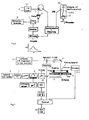
- the microwaves are generated by generator G, e.g. B. a detunable Gunn diode or a klystron. You get through an insulator I, a waveguide C, a circulator or directional coupler K and a whiten waveguide A to the sample holder S.
- the microwaves reflected by the measurement object in the sample holder S go back to the circulator (directional coupler K), and the reflected power passes through the waveguide E to the detector D1 (semiconductor diode or thermistor) and is measured there.
- the detector D1 semiconductor diode or thermistor
- the waveguides B and C are not necessary in every case and can be omitted under certain circumstances.
- the sample material can be irradiated from one side or the other with light or electrons. 2, 3, 4, three variants are shown.
- the variants according to FIGS. 2 and 3 relate to the irradiation of the samples for reflection measurements.
- the samples, which each cover or cover the waveguide cross section, can therefore be irradiated from the side facing away from the microwave field - FIG. 2 - or towards the side - FIG. 3.
- the waveguide can of course also be straight, ie. H. it need not be designed as manifold A.
- an irradiation window W1 is to be provided in the manifold A, through which the radiation reaches the sample surface. If the radiation is to strike perpendicularly, the radiation window must accordingly be provided in the area of the normal projection of the center M of the waveguide cross-sectional area which is covered by the sample, in the outer wall of the bend A.
- either radiation can also be used 3 take place, in which case the waveguide B need not be designed as a manifold.
- the variant shown in FIG. 4 does not require the waveguide A to be designed, but rather the waveguide B as a manifold and an irradiation window W2 corresponding to the manifold A and the irradiation window W1 to be provided there, see FIG. Fig. 3.
- the sample or the sample holder is then firmly positioned between the waveguides A and B, z. B. screwed in between.
- materials whose properties can be measured here are generally two-dimensional plates or layers. These are therefore placed on the cross-sectional area of the waveguide A or pressed there. If the dimensions of the measurement object are smaller than that of the waveguide cross-sectional area, it can be mounted on a support plate P, optionally provided with one or more holes, for. B. made of plastic.
- a metal cover plate R can be located behind the sample to enlarge the signal. This too can be provided with one or more holes, which is absolutely necessary if the excess microwave transmission is measured or if the measurement object is irradiated with light or electrons from a side on which metal is located.
- a plastic plate which may be provided with holes, can also be attached behind the sample.
- the apparatus for measuring the local dependence of the excess conductivity contains in particular a device with which the sample can be displaced over the cross-sectional area of the waveguide A.
- the end of the waveguide A, the cross-sectional area z. B. for reflection measurements with the test object / sample 0 till is covered, is held axially displaceably in a table top N by means of a body L for securing the position.
- the sample holder S can be formed, for example, from a two-part frame, the upper part of which has a milled channel - gauge - which carries vacuum or negative pressure. Bores are made in the lower part so that a support plate P, possibly also a plate-shaped measurement object O, adheres to the sample holder S.
- Objects 0 with smaller dimensions are placed on the support plate P and, if necessary, covered with a plate R made of metal.
- a waveguide B can be arranged above the sample holder S, which is also held axially displaceably in a table N by means of a body L for securing the position.
- the waveguide B with its open cross-sectional area is brought close to the surface of the measurement object 0.
- an intermediate layer Z, z. B. a quartz plate with 0.1 mm to 1 mm, preferably 0.5 mm thick, inserted. These then take the place of the sample 0 and cover plate R already drawn in the sample holder S.
- the sharply focused photon or electron beam arrives from an irradiation source Q via the beam steering system T to the object under test 0 (see also FIGS. 2, 3, 4).
- the sample holder S is connected via a linkage to an adjusting device XY, so that the sample 0 can be moved back and forth in the area of the cross-sectional area of the waveguide A or B and can be irradiated at various points. Because of the big difference union conditions in the microwave field, it is better to hold the local position of the respective irradiated spot on the surface of the sample 0 and the M eßob- ject of time travel over the cross sectional area of the waveguide A and B, respectively.
- the beam steering system T should at least allow pivoting movements for this.
- the irradiated spot can also be moved over the surface of the measurement object 0 in this way, or both movements - that of the sample holder S and that of the beam steering system T - can be superimposed.
- FIG. 6 and 7 schematically and in simplified form show a microwave measuring apparatus or a test setup for the location-based or location-time-based determination of structures, structural defects and the like of inhomogeneous semiconductor layers.
- Fig. 6 it can be seen that both photons - CW laser as radiation source Q1 and mechanical-optical beam steering system T1 - as well as electrons - electron beam tube Q2 and electro-magnetic system for beam steering T2 and focusing F2 - are used to irradiate a sample O. can.
- the values measured by the detector D1 as reflections from microwaves and precisely assigned to the relevant irradiated areas of the samples O are averaged via a synchronizer and a control and z. B. shown or displayed graphically.
- FIG. 7 shows in particular a shutter V in the beam path between photon beam source Q 1 and an optical focusing device F1, which also enables time-resolved measurements. Furthermore, an attenuator for the microwave power is provided, for example, between isolator I and circulator or directional coupler K in order to overdrive the de Avoid detector D1 or to be able to set the most favorable range of differently sensitive detectors D1.
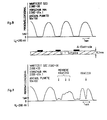
- the measurement curves shown in FIGS. 8 and 9 were recorded by Si semiconductor wafers, 0.3 mm thick, with a diameter of approx. 50 mm, i. H. approx. 2000 mm2 surface, on which circular Al electrodes with a diameter of 1 mm were applied.
- the microwave signal indicates - Fig. 8 - where the electrodes are and - Fig. 9 - where the surface of the Si and Al is damaged - here by deliberately applied scratches.
- the location of the irradiated area was fixed with respect to the microwave field, i. H. the sample is shifted over the waveguide cross-sectional area and the beam direction is not changed. Only relative changes in microwave reflection or transmission as a result of additionally excited charge carriers in the sample material in the area of the irradiated spot (approx. 0.1 ⁇ m to 10 ⁇ m diameter) are evaluated.
- This charge carrier intensity is dependent on the structure of the sample or its surface, so that, for. B. with X-Y shifts in the pm range a sufficiently high resolution to determine microstructures / structural defects u. Like. is achievable.
- a computer can be used for the measurements and their evaluation.
- Embodiments of the invention can also be integrated as a microwave detection system in commercial scanning electron microscopes.
Landscapes
- Physics & Mathematics (AREA)
- General Physics & Mathematics (AREA)
- Pathology (AREA)
- Life Sciences & Earth Sciences (AREA)
- Chemical & Material Sciences (AREA)
- Analytical Chemistry (AREA)
- Biochemistry (AREA)
- Health & Medical Sciences (AREA)
- General Health & Medical Sciences (AREA)
- Immunology (AREA)
- Electromagnetism (AREA)
- Testing Or Measuring Of Semiconductors Or The Like (AREA)
- Analysing Materials By The Use Of Radiation (AREA)
- Testing Of Individual Semiconductor Devices (AREA)
- Tests Of Electronic Circuits (AREA)
- Investigating Or Analyzing Non-Biological Materials By The Use Of Chemical Means (AREA)
- Investigating Or Analyzing Materials By The Use Of Electric Means (AREA)
Priority Applications (1)
| Application Number | Priority Date | Filing Date | Title |
|---|---|---|---|
| AT85730027T ATE64206T1 (de) | 1984-02-29 | 1985-02-26 | Verfahren und apparaturen zum untersuchen von photoempfindlichen materialien mittels mikrowellen. |
Applications Claiming Priority (2)
| Application Number | Priority Date | Filing Date | Title |
|---|---|---|---|
| DE3407850 | 1984-02-29 | ||
| DE19843407850 DE3407850A1 (de) | 1984-02-29 | 1984-02-29 | Mikrowellen-messverfahren und -messapparatur zur kontaktlosen und zerstoerungsfreien untersuchung photoempfindlicher materialien |
Publications (3)
| Publication Number | Publication Date |
|---|---|
| EP0155225A2 true EP0155225A2 (fr) | 1985-09-18 |
| EP0155225A3 EP0155225A3 (en) | 1989-01-25 |
| EP0155225B1 EP0155225B1 (fr) | 1991-06-05 |
Family
ID=6229485
Family Applications (1)
| Application Number | Title | Priority Date | Filing Date |
|---|---|---|---|
| EP85730027A Expired - Lifetime EP0155225B1 (fr) | 1984-02-29 | 1985-02-26 | Méthode et appareils pour l'analyse de matériaux photosensibles à l'aide de microondes |
Country Status (6)
| Country | Link |
|---|---|
| US (1) | US4704576A (fr) |
| EP (1) | EP0155225B1 (fr) |
| JP (1) | JPH0731139B2 (fr) |
| AT (1) | ATE64206T1 (fr) |
| CA (1) | CA1234927A (fr) |
| DE (2) | DE3407850A1 (fr) |
Families Citing this family (35)
| Publication number | Priority date | Publication date | Assignee | Title |
|---|---|---|---|---|
| HU196262B (en) * | 1986-03-17 | 1988-10-28 | Mta Mueszaki Fiz Kutato Inteze | Method for testing electrically active impuritles in semiconductor materials and structures and measuring arrangement for implementing method |
| DE3619314A1 (de) * | 1986-06-09 | 1987-12-10 | Hahn Meitner Kernforsch | Mikrowellen-messapparatur |
| JPS63119542A (ja) * | 1986-11-07 | 1988-05-24 | Toshiba Corp | 2次電子取込み装置 |
| WO1990005908A1 (fr) * | 1988-11-18 | 1990-05-31 | Magyar Tudományos Akadémia Müszaki Fizikai Kutató Intézete | Procede et appareil ameliores pour spectroscopie, par transitoires de micro-ondes, des niveaux profonds dans des semi-conducteurs |
| US5081414A (en) * | 1989-03-20 | 1992-01-14 | Semitex Co., Ltd. | Method for measuring lifetime of semiconductor material and apparatus therefor |
| US4902967A (en) * | 1989-05-18 | 1990-02-20 | The United States Of America As Represented By The Secretary Of The Navy | Scanning electron microscopy by photovoltage contrast imaging |
| FR2647223B1 (fr) * | 1989-05-22 | 1991-08-30 | Europ Propulsion | Dispositif de mesure de caracteristique electromagnetique d'un materiau a tres haute temperature |
| JPH0518896A (ja) * | 1990-02-22 | 1993-01-26 | Heinrich Hertz Inst Nachrichtentech Berlin Gmbh | 小さな吸光量の検出用測定方法 |
| US5103182A (en) * | 1990-04-02 | 1992-04-07 | Texas Instruments Incorporated | Electromagnetic wave measurement of conductive layers of a semiconductor wafer during processing in a fabrication chamber |
| JP2702807B2 (ja) * | 1990-08-09 | 1998-01-26 | 東芝セラミックス株式会社 | 半導体中の深い不純物準位の測定方法及びその装置 |
| HUT63497A (en) * | 1990-12-17 | 1993-08-30 | Semilab Felvezetoe Fiz Lab Rt | Method and apparatus for measuring minority charge carrier in semiconductor material |
| US5406214A (en) * | 1990-12-17 | 1995-04-11 | Semilab Felvezeto Fizikai Lab, Rt | Method and apparatus for measuring minority carrier lifetime in semiconductor materials |
| US5270222A (en) * | 1990-12-31 | 1993-12-14 | Texas Instruments Incorporated | Method and apparatus for semiconductor device fabrication diagnosis and prognosis |
| JP3121938B2 (ja) * | 1992-05-14 | 2001-01-09 | 株式会社神戸製鋼所 | 半導体ウエハの少数キャリアのライフタイム測定装置 |
| JPH07105427B2 (ja) * | 1992-10-19 | 1995-11-13 | 学校法人幾徳学園 | 半導体材料のライフタイム評価方法とその装置 |
| US5519193A (en) * | 1992-10-27 | 1996-05-21 | International Business Machines Corporation | Method and apparatus for stressing, burning in and reducing leakage current of electronic devices using microwave radiation |
| US5434505A (en) * | 1993-07-30 | 1995-07-18 | Litton Systems, Inc. | Method and apparatus for low temperature HEMT-like material testing |
| US5521839A (en) * | 1993-09-02 | 1996-05-28 | Georgia Tech Research Corporation | Deep level transient spectroscopy (DLTS) system and method |
| US5563067A (en) | 1994-06-13 | 1996-10-08 | Matsushita Electric Industrial Co., Ltd. | Cell potential measurement apparatus having a plurality of microelectrodes |
| USRE40209E1 (en) | 1994-06-13 | 2008-04-01 | Matsushita Electric Industrial Co., Ltd. | Cell potential measurement apparatus having a plurality of microelectrodes |
| US5508630A (en) * | 1994-09-09 | 1996-04-16 | Board Of Regents, University Of Texas Systems | Probe having a power detector for use with microwave or millimeter wave device |
| JP3670051B2 (ja) * | 1995-06-06 | 2005-07-13 | 株式会社神戸製鋼所 | 半導体試料のキャリアのライフタイム測定方法及びその装置 |
| JP2930182B2 (ja) * | 1995-06-20 | 1999-08-03 | 松下電器産業株式会社 | 神経細胞活動測定用2次元センサ及びこれを用いた測定装置 |
| JP2930181B2 (ja) * | 1995-06-20 | 1999-08-03 | 松下電器産業株式会社 | 神経細胞活動測定用2次元センサ及びこれを用いた測定装置 |
| US5886534A (en) * | 1995-10-27 | 1999-03-23 | The University Of Chicago | Millimeter wave sensor for on-line inspection of thin sheet dielectrics |
| US5767693A (en) * | 1996-09-04 | 1998-06-16 | Smithley Instruments, Inc. | Method and apparatus for measurement of mobile charges with a corona screen gun |
| US5867034A (en) * | 1997-01-30 | 1999-02-02 | Sokolov; Vladimir | Non-destructive method and apparatus for monitoring carrier lifetime of a semiconductor sample during fabrication |
| US6060709A (en) * | 1997-12-31 | 2000-05-09 | Verkuil; Roger L. | Apparatus and method for depositing uniform charge on a thin oxide semiconductor wafer |
| HUP9902355A2 (hu) * | 1999-07-12 | 2001-07-30 | SEMILAB Félvezető Fizikai Laboratórium Rt. | Nagy érzékenységű eljárás és berendezés kisebbségi töltéshordozók élettartamának mérésére félvezető anyagokban |
| HU227170B1 (en) * | 2000-02-17 | 2010-09-28 | Semilab Felvezetoe Fiz Lab Rt | Surface passivation method and arrangement for measuring life time of minority carrier of semiconductors |
| US7482072B2 (en) * | 2002-07-09 | 2009-01-27 | Grintellectual Reserve, Llc | Optimizing reactions in fuel cells and electrochemical reactions |
| DE102006051577B4 (de) | 2006-11-03 | 2011-07-21 | Deutsche Solar AG, 09599 | Vorrichtung und Verfahren zur Erfassung elektrischer Eigenschaften einer Probe aus einem anregbaren Material |
| US7725783B2 (en) * | 2007-07-20 | 2010-05-25 | International Business Machines Corporation | Method and apparatus for repeatable drive strength assessments of high speed memory DIMMs |
| JP5350345B2 (ja) * | 2010-09-22 | 2013-11-27 | 株式会社神戸製鋼所 | 薄膜半導体の結晶性評価装置および方法 |
| CN116930799B (zh) * | 2023-09-15 | 2023-12-08 | 江苏森标科技有限公司 | 一种电池片在线方阻检测系统 |
Family Cites Families (3)
| Publication number | Priority date | Publication date | Assignee | Title |
|---|---|---|---|---|
| JPS5236817B2 (fr) * | 1973-07-27 | 1977-09-19 | ||
| JPS54160133A (en) * | 1978-06-09 | 1979-12-18 | Toshiba Corp | Test unit for paper-like object |
| JPS57112041A (en) * | 1980-12-29 | 1982-07-12 | Fujitsu Ltd | Evaluation for silicon single crystal |
-
1984
- 1984-02-29 DE DE19843407850 patent/DE3407850A1/de not_active Ceased
-
1985
- 1985-02-26 EP EP85730027A patent/EP0155225B1/fr not_active Expired - Lifetime
- 1985-02-26 DE DE8585730027T patent/DE3583048D1/de not_active Expired - Lifetime
- 1985-02-26 AT AT85730027T patent/ATE64206T1/de not_active IP Right Cessation
- 1985-02-28 CA CA000475476A patent/CA1234927A/fr not_active Expired
- 1985-02-28 US US06/706,712 patent/US4704576A/en not_active Expired - Fee Related
- 1985-02-28 JP JP60037810A patent/JPH0731139B2/ja not_active Expired - Lifetime
Also Published As
| Publication number | Publication date |
|---|---|
| JPS60203840A (ja) | 1985-10-15 |
| DE3407850A1 (de) | 1985-09-05 |
| US4704576A (en) | 1987-11-03 |
| ATE64206T1 (de) | 1991-06-15 |
| CA1234927A (fr) | 1988-04-05 |
| JPH0731139B2 (ja) | 1995-04-10 |
| DE3583048D1 (de) | 1991-07-11 |
| EP0155225B1 (fr) | 1991-06-05 |
| EP0155225A3 (en) | 1989-01-25 |
Similar Documents
| Publication | Publication Date | Title |
|---|---|---|
| EP0155225B1 (fr) | Méthode et appareils pour l'analyse de matériaux photosensibles à l'aide de microondes | |
| DE3885575T2 (de) | Vorrichtung zur Analyse mittels Röntgenstrahlen. | |
| DE69933753T2 (de) | Verbessertes verfahren und vorrichtung zur schichtdickenbestimmung | |
| DE68921008T2 (de) | Photonenabtasttunneleffektmikroskop. | |
| DE69223088T2 (de) | Apparat zur Musterüberprüfung und Elektronenstrahlgerät | |
| DE102010034666B4 (de) | Röntgenanalysevorrichtung und Röntgenanalyseverfahren | |
| DE69103783T2 (de) | Verfahren und Vorrichtung zum Messen der Dicke einer Schicht. | |
| DE19609521C2 (de) | Abtastanalysator für photoinduzierten Strom mit der Fähigkeit photoinduzierten Strom in nicht-vorgespannten Proben nachzuweisen | |
| DE102004045145B4 (de) | Verfahren zur Kristallorientierungsmessung mittels Röntgenstrahlung und Vorrichtung zur Kristallorientierungsmessung mittels Röntgenstrahlung | |
| DE69609336T2 (de) | Nahfeld-leitfähigkeits-mikroskop | |
| DE102016222187A1 (de) | Verfahren zum Bestimmen eines Strahlprofils eines Laserstrahls und Bearbeitungsmaschine | |
| DE102014212563B4 (de) | Messvorrichtung und Verfahren zum Bestimmen einer Positionsänderung eines Teilchenstrahls eines Rasterteilchenmikroskops | |
| DE2554898C2 (de) | Verfahren und Vorrichtung zur akustischen Abbildung | |
| DE4015893A1 (de) | Vorrichtung zur beruehrungslosen und zerstoerungsfreien untersuchung der inneren und/oder aeusseren struktur absorptionsfaehiger prueflinge | |
| DE102007056944A1 (de) | Lumineszenz-Messgerät zur ortsaufgelösten Messung von Halbleiterproben | |
| EP0176745A1 (fr) | Dispositif et procédé pour mesurer des longueurs dans un microscope corpusculaire à balayage | |
| EP0443702A2 (fr) | Procédé de mesure pour déterminer de petites absorptions de lumière | |
| DE19882660B4 (de) | Optisches Verfahren für die Kennzeichnung der elektrischen Eigenschaften von Halbleitern und Isolierfilmen | |
| EP2097761B1 (fr) | Dispositif et procédé de détermination de propriétés électriques d'un échantillon en matériau excitable | |
| DE3926945A1 (de) | Vorrichtung zum messen der dauer einzelner kurzer optischer strahlungsimpulse | |
| DE19706973A1 (de) | Vorrichtung und Verfahren zur Untersuchung einer glatten Oberfläche einer Probe | |
| DE112015006104B4 (de) | Elektronenmikroskop | |
| DE4404154A1 (de) | Verfahren und Vorrichtung zum optischen Untersuchen einer Oberfläche | |
| WO2006000501A1 (fr) | Procede et dispositif de mesure d'un profil de faisceau d'un faisceau laser et dispositif de traitement au laser | |
| EP3426429A1 (fr) | Procédé de détermination de la position du foyer d'un dispositif de rayonnement laser et procédé d'usinage d'une pièce de travail avec un rayonnement laser |
Legal Events
| Date | Code | Title | Description |
|---|---|---|---|
| PUAI | Public reference made under article 153(3) epc to a published international application that has entered the european phase |
Free format text: ORIGINAL CODE: 0009012 |
|
| AK | Designated contracting states |
Designated state(s): AT BE CH DE FR GB IT LI LU NL SE |
|
| RAP1 | Party data changed (applicant data changed or rights of an application transferred) |
Owner name: HAHN-MEITNER-INSTITUT BERLIN GESELLSCHAFT MIT BESC |
|
| PUAL | Search report despatched |
Free format text: ORIGINAL CODE: 0009013 |
|
| AK | Designated contracting states |
Kind code of ref document: A3 Designated state(s): AT BE CH DE FR GB IT LI LU NL SE |
|
| 17P | Request for examination filed |
Effective date: 19890614 |
|
| 17Q | First examination report despatched |
Effective date: 19901107 |
|
| GRAA | (expected) grant |
Free format text: ORIGINAL CODE: 0009210 |
|
| AK | Designated contracting states |
Kind code of ref document: B1 Designated state(s): AT BE CH DE FR GB IT LI LU NL SE |
|
| REF | Corresponds to: |
Ref document number: 64206 Country of ref document: AT Date of ref document: 19910615 Kind code of ref document: T |
|
| ITF | It: translation for a ep patent filed | ||
| REF | Corresponds to: |
Ref document number: 3583048 Country of ref document: DE Date of ref document: 19910711 |
|
| GBT | Gb: translation of ep patent filed (gb section 77(6)(a)/1977) | ||
| ET | Fr: translation filed | ||
| PLBE | No opposition filed within time limit |
Free format text: ORIGINAL CODE: 0009261 |
|
| STAA | Information on the status of an ep patent application or granted ep patent |
Free format text: STATUS: NO OPPOSITION FILED WITHIN TIME LIMIT |
|
| 26N | No opposition filed | ||
| EPTA | Lu: last paid annual fee | ||
| EAL | Se: european patent in force in sweden |
Ref document number: 85730027.1 |
|
| PGFP | Annual fee paid to national office [announced via postgrant information from national office to epo] |
Ref country code: NL Payment date: 19960331 Year of fee payment: 12 |
|
| PGFP | Annual fee paid to national office [announced via postgrant information from national office to epo] |
Ref country code: BE Payment date: 19960401 Year of fee payment: 12 |
|
| PGFP | Annual fee paid to national office [announced via postgrant information from national office to epo] |
Ref country code: DE Payment date: 19960426 Year of fee payment: 12 |
|
| PGFP | Annual fee paid to national office [announced via postgrant information from national office to epo] |
Ref country code: GB Payment date: 19960514 Year of fee payment: 12 |
|
| PGFP | Annual fee paid to national office [announced via postgrant information from national office to epo] |
Ref country code: CH Payment date: 19960604 Year of fee payment: 12 |
|
| PGFP | Annual fee paid to national office [announced via postgrant information from national office to epo] |
Ref country code: LU Payment date: 19960801 Year of fee payment: 12 |
|
| PGFP | Annual fee paid to national office [announced via postgrant information from national office to epo] |
Ref country code: SE Payment date: 19960812 Year of fee payment: 12 |
|
| PGFP | Annual fee paid to national office [announced via postgrant information from national office to epo] |
Ref country code: AT Payment date: 19960814 Year of fee payment: 12 Ref country code: FR Payment date: 19960814 Year of fee payment: 12 |
|
| PG25 | Lapsed in a contracting state [announced via postgrant information from national office to epo] |
Ref country code: AT Effective date: 19970226 Ref country code: LU Free format text: LAPSE BECAUSE OF NON-PAYMENT OF DUE FEES Effective date: 19970226 Ref country code: GB Effective date: 19970226 |
|
| PG25 | Lapsed in a contracting state [announced via postgrant information from national office to epo] |
Ref country code: SE Effective date: 19970227 |
|
| PG25 | Lapsed in a contracting state [announced via postgrant information from national office to epo] |
Ref country code: BE Effective date: 19970228 Ref country code: CH Effective date: 19970228 Ref country code: LI Effective date: 19970228 |
|
| BERE | Be: lapsed |
Owner name: HAHN-MEITNER-INSTITUT BERLIN G.M.B.H. Effective date: 19970228 |
|
| PG25 | Lapsed in a contracting state [announced via postgrant information from national office to epo] |
Ref country code: NL Effective date: 19970901 |
|
| GBPC | Gb: european patent ceased through non-payment of renewal fee |
Effective date: 19970226 |
|
| REG | Reference to a national code |
Ref country code: CH Ref legal event code: PL |
|
| PG25 | Lapsed in a contracting state [announced via postgrant information from national office to epo] |
Ref country code: FR Effective date: 19971030 |
|
| PG25 | Lapsed in a contracting state [announced via postgrant information from national office to epo] |
Ref country code: DE Effective date: 19971101 |
|
| EUG | Se: european patent has lapsed |
Ref document number: 85730027.1 |
|
| NLV4 | Nl: lapsed or anulled due to non-payment of the annual fee |
Effective date: 19970901 |
|
| REG | Reference to a national code |
Ref country code: FR Ref legal event code: ST |