EP0155283B1 - Ionenstrahlkolonne mit brennpunkt - Google Patents
Ionenstrahlkolonne mit brennpunkt Download PDFInfo
- Publication number
- EP0155283B1 EP0155283B1 EP84903206A EP84903206A EP0155283B1 EP 0155283 B1 EP0155283 B1 EP 0155283B1 EP 84903206 A EP84903206 A EP 84903206A EP 84903206 A EP84903206 A EP 84903206A EP 0155283 B1 EP0155283 B1 EP 0155283B1
- Authority
- EP
- European Patent Office
- Prior art keywords
- lens
- ion beam
- ion
- source
- beam column
- Prior art date
- Legal status (The legal status is an assumption and is not a legal conclusion. Google has not performed a legal analysis and makes no representation as to the accuracy of the status listed.)
- Expired
Links
- 238000010884 ion-beam technique Methods 0.000 title claims abstract description 36
- 229910001338 liquidmetal Inorganic materials 0.000 claims abstract description 13
- 150000002500 ions Chemical class 0.000 claims description 33
- 230000004075 alteration Effects 0.000 claims description 16
- 229910052710 silicon Inorganic materials 0.000 claims description 13
- 239000010703 silicon Substances 0.000 claims description 13
- 230000001133 acceleration Effects 0.000 claims description 10
- XUIMIQQOPSSXEZ-UHFFFAOYSA-N Silicon Chemical compound [Si] XUIMIQQOPSSXEZ-UHFFFAOYSA-N 0.000 claims description 9
- 230000005684 electric field Effects 0.000 claims description 5
- 239000002245 particle Substances 0.000 claims description 4
- -1 silicon ions Chemical class 0.000 claims description 4
- 229910045601 alloy Inorganic materials 0.000 claims description 2
- 239000000956 alloy Substances 0.000 claims description 2
- PCHJSUWPFVWCPO-UHFFFAOYSA-N gold Chemical compound [Au] PCHJSUWPFVWCPO-UHFFFAOYSA-N 0.000 claims description 2
- 239000010931 gold Substances 0.000 claims description 2
- 229910001020 Au alloy Inorganic materials 0.000 claims 1
- 229910000676 Si alloy Inorganic materials 0.000 claims 1
- 239000012212 insulator Substances 0.000 description 4
- 238000000926 separation method Methods 0.000 description 4
- 238000002955 isolation Methods 0.000 description 2
- 239000012528 membrane Substances 0.000 description 2
- 201000009310 astigmatism Diseases 0.000 description 1
- 238000010586 diagram Methods 0.000 description 1
- 230000000694 effects Effects 0.000 description 1
- 239000006023 eutectic alloy Substances 0.000 description 1
- 230000005496 eutectics Effects 0.000 description 1
- 238000000605 extraction Methods 0.000 description 1
- 229910052737 gold Inorganic materials 0.000 description 1
- 239000012535 impurity Substances 0.000 description 1
- 238000002164 ion-beam lithography Methods 0.000 description 1
- 239000000463 material Substances 0.000 description 1
- 229910052751 metal Inorganic materials 0.000 description 1
- 230000003287 optical effect Effects 0.000 description 1
- 229920002120 photoresistant polymer Polymers 0.000 description 1
- XUIMIQQOPSSXEZ-IGMARMGPSA-N silicon-28 atom Chemical compound [28Si] XUIMIQQOPSSXEZ-IGMARMGPSA-N 0.000 description 1
- 239000000758 substrate Substances 0.000 description 1
Images


Classifications
-
- H—ELECTRICITY
- H01—ELECTRIC ELEMENTS
- H01J—ELECTRIC DISCHARGE TUBES OR DISCHARGE LAMPS
- H01J37/00—Discharge tubes with provision for introducing objects or material to be exposed to the discharge, e.g. for the purpose of examination or processing thereof
- H01J37/30—Electron-beam or ion-beam tubes for localised treatment of objects
- H01J37/3002—Details
- H01J37/3007—Electron or ion-optical systems
Definitions
- This invention is directed to a focused ion beam column particularly useful for scanning a small spot over a large field for the exposure of resist material.
- the column has the capability of exposing images smaller than 0.1 micrometer (micron) and has the capability of addressing a field of about 1 millimeter square at the target while maintaining the aberration limited spot size to less than about 0.1 pm.
- a two lens focused ion beam column comprising an ion source for producing charged ionic particles of a desired ion species.
- An acceleration electrode is used for extracting the positively charged ion particles to form an ion beam.
- a first accelerating lens focuses the desired ion species in the ion beam onto an analyzer slit.
- a second accelerating lens which demagnifies the beam is positioned downstream from the analyzer slit and focuses the beam of desired ion species onto a target plane.
- a deflector is positioned between the downstream, second lens and a target plane for reflecting the beam over a pattern of the desired plane. The diameter of the focused ion beam thereby is less than 0.1 pm, which is 1000 A.
- the two lens focused ion beam column known from this reference and being the generic art, has a scanfield which is also restricted to very small dimensions, so that only a small field can be scanned. This limited scanfield arises from a short working distance associated with the final lens.
- an object of the present invention to provide a two lens focused ion beam column, according to the pre-characterizing part of claim 1, wherein a small spot size can be scanned over a large field.
- the ion beam column has features which permit exposing small images on large scanfields to reduce the time lost in stepping between scanfields to provide a high rate of wafer exposure. The large scanfield eliminates the time and accuracy lost due to extra reregistration.
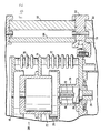
- Fig. 1 shows the ion beam column 10 of this invention as being mounted on a target chamber 12.
- Fig. 3 schematically illustrates the column 10 and shows its ion source 14 which produces an ion beam 16.
- Accelerator electrode 18 forms the first element of the three element first lens 20.
- the second and third elements 22 and 24 are seen in Figs. 1, 2 and 3.
- the first lens 20 is an asymmetric lens as illustrated in Figs. 1, 2 and 3.
- Asymmetric lens 20 focuses the ion beams 16 at mass analyzer slit 26.
- ExB mass separator 28 has its electric field plates shown in Figs. 1, 2 and 3. They lie perpendicular to the plane of the paper with their electric field gradient in the plane of the paper.
- a magnetic field perpendicular to the plane of the paper in the space between the electric field plates is supplied in a conventional manner.
- the electric and magnetic field strengths are arranged so that the desired species proceeds on a straight line along the axis of the column, as is indicated in Fig. 3.
- a membrane with analyzer slit 26 is positioned downstream on the axis so that the desired species passes through the slit and the undesired species is collected on the membrane around the slit.
- Alignment deflector 34 is positioned downstream of the slit 26 in order to maintain the beam of desired species on the axis.
- Demagnifying and accelerating lens 36 is positioned downstream on the axis of the ion beam.
- a Munro lens is illustrated as preferred. It is the second lens in the column and comprises first and second lens elements 38 and 40. Downstream from the Munro lens 36 is deflector 42 which serves as a device to deflect the beam so that it scans the field on target 44, see Fig. 3.
- Ion source 14 is a liquid metal ion source.
- the variety of ions available from liquid metal ion sources has recently been extended by the introduction of alloys, especially eutectic alloys of metallic elements.
- the liquid metal ion sources disclosed in U.S. Patents 4,318,029 and 4,318,030 can be employed as the source 14.
- Silicon is the preferred ion for exposure because it can be doubly charged and does not introduce impurities in the silicon target under the resist being exposed.
- the doubly charged silicon ion beam can be produced from an 80%/20% gold/silicon eutectic.
- the ion beam 16 is extracted from the source by means of acceleration electrode 18 which serves as the first element of asymmetric lens 20.
- the variation in the potential at which the silicon ions are created in the liquid metal cusp in the source represents the dominant factor in determining the minimum achievable spot size at the target.
- This potential variation or chromatic spread arises from the large potential gradients at the liquid metal cusp and has been characterized to be between 6 and 14 volts, with 10 volts being typical.
- the asymmetric lens 20 is used to image the emitting tip of the liquid metal source 14 at the separation slit 26. This decouples the beam properties at the slit 26 from variations in the extraction voltage.
- Asymmetric lens 20 operates at a voltage ratio of about 4 to produce an acceleration potential of 40 kilovolts prior to mass separation. The lens shape and spacing is such that with this potential the lens magnification is very near unity so that an aberration limited spot size of less than about 500 nm is achieved at the focus point of lens 20 at the separation slit 26.
- the ExB mass separator 28 separates the doubly charged silicon ions from the other ionic species in the beam.
- This type of device has the advantage of alignment on the optical axis and is of simple design.
- the electric and magnetic fields are as weak as possible to completely resolve doubly charged silicon from the nearest lying beam component which is singly charged silicon.
- the mass 29 and mass 30 isotopes of silicon are discriminated against by using the exposure characteristics of the photoresist on the target and also by isotopically enriching the silicon source to at least 99% silicon 28.
- the chromatic aberration introduced by the Ex B fields under these conditions are less than 40 nm at the mass separation slit 26 and this aberration is negligible compared to the contributions from the asymmetric lens 20.
- the final beam focusing is performed by the accelerating and demagnifying Munro lens 36, operating at a voltage ratio of 4 to 1.
- the lens spacing and shape is such that magnification under these conditions is 0.161, such that the overall system magnification is less than about 0.17. This minimizes the effect on spot size which results from the finite source size.
- the aberration limited beam spot size, when the beam is on axis at the target, for this combination of lenses, is about 70 nm for typical source operation, when the chromatic spread of the source is 10 volts and is about 98.3 nm when chromatic spread is 14 volts, the worst case.
- lens demagnification is required in the second lens 36, so that there is a large working distance between the second lens element 40 of Munro lens 36 and the target.
- the small beam divergence a 2 out of the first lens allows a long drift region between lenses.
- the long working distance out of the second lens permits the use of a long deflector 42 to achieve significant scanfield size up to about 1 millimeter square, while maintaining relatively small deflection angles, below 10 milliradians and with reasonable deflection voltages, for example less than 150 volts. These factors are critical in reducing scan related aberrations from field curvature, astigmatism and distortion.
- Table I describes a particular example of an embodiment of this invention.
- the figures are for a worst case chromatic aberration of 14 volts.
- the beam diameter total is the on-axis beam.
- lens 1 has a magnification near unity.
- Table II gives an example of a desired scanfield and the aberration that results from that scanfield.
- Fig. 3 shows the power supplies which provide the various potentials shown in Table III.
- the principal high voltage power supply 46 provides 120 KV potential to the floating frame 47 on which power supplies 52-60 are mounted and are referenced. Power to the supplies is provided through isolation transformer 50.
- Deflection power supply 48 provides the differential voltages necessary for beam deflection.
- Power supply 60 provides the cathode voltage and heater supply potential to ion source 14.
- Figs. 1 and 2 show the physical column structure by which the portions of the column system are held in alignment.
- ion source 14 is mounted on column cap 62.
- the lower edge of the cap carries annular grooves in which are fitted insulator tubes 64 and 66.
- Center plate 68 carries drift tube 70 thereunder, which at its lower end carries the first lens element 38 of Munro lens 36.
- Center plate 68 is at the potential of lens element 38.
- the analyzer plate carrying mass analyzer slit 26 is also mounted on center plate 68 and is at the potential of lens element 38.
- the third element 24 of asymmetric lens 30 and the ExB mass separator 28 are mounted on the center plate to lie at the same potential.
- ExB mass separator 28 has its field plates floating with respect to that potential to apply a transverse electric field.
- Insulators 72 carry support ring 74 which in turn carries therethrough the inverted cup-shaped second element 22 of asymmetric lens 20.
- Insulators 76 are mounted on the top of support ring 74 and carry thereon the accelerator electrode 18.
- Insulator tubes 78 and 80 are engaged between center plate 68 and the base ring 82, which in turn mounts on target chamber 12.
Landscapes
- Chemical & Material Sciences (AREA)
- Analytical Chemistry (AREA)
- Electron Sources, Ion Sources (AREA)
- Electron Beam Exposure (AREA)
Claims (9)
Priority Applications (1)
| Application Number | Priority Date | Filing Date | Title |
|---|---|---|---|
| AT84903206T ATE35347T1 (de) | 1983-07-12 | 1984-06-25 | Ionenstrahlkolonne mit brennpunkt. |
Applications Claiming Priority (2)
| Application Number | Priority Date | Filing Date | Title |
|---|---|---|---|
| US06/512,879 US4556798A (en) | 1983-07-12 | 1983-07-12 | Focused ion beam column |
| US512879 | 1983-07-12 |
Publications (2)
| Publication Number | Publication Date |
|---|---|
| EP0155283A1 EP0155283A1 (de) | 1985-09-25 |
| EP0155283B1 true EP0155283B1 (de) | 1988-06-22 |
Family
ID=24040992
Family Applications (1)
| Application Number | Title | Priority Date | Filing Date |
|---|---|---|---|
| EP84903206A Expired EP0155283B1 (de) | 1983-07-12 | 1984-06-25 | Ionenstrahlkolonne mit brennpunkt |
Country Status (6)
| Country | Link |
|---|---|
| US (1) | US4556798A (de) |
| EP (1) | EP0155283B1 (de) |
| JP (1) | JPH0628145B2 (de) |
| CA (1) | CA1214577A (de) |
| DE (1) | DE3472331D1 (de) |
| WO (1) | WO1985000693A1 (de) |
Families Citing this family (17)
| Publication number | Priority date | Publication date | Assignee | Title |
|---|---|---|---|---|
| KR890002747B1 (ko) * | 1983-11-07 | 1989-07-26 | 가부시기가이샤 히다찌세이사꾸쇼 | 이온 빔에 의한 성막방법 및 그 장치 |
| JPS60243960A (ja) * | 1984-05-18 | 1985-12-03 | Hitachi Ltd | イオンマイクロビ−ム装置 |
| JPS61237421A (ja) * | 1985-04-15 | 1986-10-22 | Hitachi Ltd | 半導体装置の製造方法 |
| JPH0685309B2 (ja) * | 1985-12-13 | 1994-10-26 | 株式会社日立製作所 | 液体金属イオン源 |
| US5035787A (en) * | 1987-07-22 | 1991-07-30 | Microbeam, Inc. | Method for repairing semiconductor masks and reticles |
| JPH071681B2 (ja) * | 1990-04-19 | 1995-01-11 | 株式会社日立製作所 | 荷電粒子線装置 |
| US5331172A (en) * | 1991-02-11 | 1994-07-19 | Microelectronics And Computer Technology Corporation | Ionized metal cluster beam systems and methods |
| US5156997A (en) * | 1991-02-11 | 1992-10-20 | Microelectronics And Computer Technology Corporation | Method of making semiconductor bonding bumps using metal cluster ion deposition |
| US5241182A (en) * | 1991-06-18 | 1993-08-31 | Fei Company | Precision electrostatic lens system and method of manufacture |
| WO1999013500A1 (fr) * | 1997-09-10 | 1999-03-18 | Hitachi, Ltd. | Appareil d'usinage par projection d'un faisceau d'ions |
| JP5033314B2 (ja) * | 2004-09-29 | 2012-09-26 | 株式会社日立ハイテクノロジーズ | イオンビーム加工装置及び加工方法 |
| WO2007008792A2 (en) * | 2005-07-08 | 2007-01-18 | Nexgensemi Holdings Corporation | Apparatus and method for controlled particle beam manufacturing |
| WO2008140585A1 (en) | 2006-11-22 | 2008-11-20 | Nexgen Semi Holding, Inc. | Apparatus and method for conformal mask manufacturing |
| JP2008166137A (ja) * | 2006-12-28 | 2008-07-17 | Sii Nanotechnology Inc | 集束イオンビーム装置 |
| US10991545B2 (en) | 2008-06-30 | 2021-04-27 | Nexgen Semi Holding, Inc. | Method and device for spatial charged particle bunching |
| US10566169B1 (en) | 2008-06-30 | 2020-02-18 | Nexgen Semi Holding, Inc. | Method and device for spatial charged particle bunching |
| US12493005B1 (en) | 2022-06-07 | 2025-12-09 | Nexgen Semi Holding, Inc. | Extended range active illumination imager |
Family Cites Families (6)
| Publication number | Priority date | Publication date | Assignee | Title |
|---|---|---|---|---|
| US3723733A (en) * | 1971-05-12 | 1973-03-27 | Hughes Aircraft Co | Stigmatic, crossed-field velocity filter |
| US3937958A (en) * | 1975-03-31 | 1976-02-10 | Minnesota Mining And Manufacturing Company | Charged particle beam apparatus |
| US4426582A (en) * | 1980-01-21 | 1984-01-17 | Oregon Graduate Center | Charged particle beam apparatus and method utilizing liquid metal field ionization source and asymmetric three element lens system |
| US4318029A (en) * | 1980-05-12 | 1982-03-02 | Hughes Aircraft Company | Liquid metal ion source |
| US4367429A (en) * | 1980-11-03 | 1983-01-04 | Hughes Aircraft Company | Alloys for liquid metal ion sources |
| JPS58500826A (ja) * | 1981-05-26 | 1983-05-19 | ヒユ−ズ・エアクラフト・カンパニ− | 集束されたイオンビ−ムを用いる精密微細加工用コラム |
-
1983
- 1983-07-12 US US06/512,879 patent/US4556798A/en not_active Expired - Lifetime
-
1984
- 1984-06-25 DE DE8484903206T patent/DE3472331D1/de not_active Expired
- 1984-06-25 JP JP59503256A patent/JPH0628145B2/ja not_active Expired - Lifetime
- 1984-06-25 WO PCT/US1984/000982 patent/WO1985000693A1/en not_active Ceased
- 1984-06-25 EP EP84903206A patent/EP0155283B1/de not_active Expired
- 1984-07-11 CA CA000458606A patent/CA1214577A/en not_active Expired
Non-Patent Citations (2)
| Title |
|---|
| Etended Abstracts, vol. 82, no. 1, May 1982, (Pennington, N.J., US), M. Komuro: "Focused ion beam using a triode gun", pages 464-465 * |
| Japanese Journal of Applied Physics, vol. 22, no. 5, part 2, May 1983, (Tokyo, JP), E. Miyauchi et al.: "A 100kV markless ion-implantation system with an Au-Si-Be liquid metal ion source for III-V compound semiconductors", pages L287-L288 * |
Also Published As
| Publication number | Publication date |
|---|---|
| US4556798A (en) | 1985-12-03 |
| JPH0628145B2 (ja) | 1994-04-13 |
| JPS60501828A (ja) | 1985-10-24 |
| WO1985000693A1 (en) | 1985-02-14 |
| EP0155283A1 (de) | 1985-09-25 |
| DE3472331D1 (en) | 1988-07-28 |
| CA1214577A (en) | 1986-11-25 |
Similar Documents
| Publication | Publication Date | Title |
|---|---|---|
| EP0155283B1 (de) | Ionenstrahlkolonne mit brennpunkt | |
| US4649316A (en) | Ion beam species filter and blanker | |
| EP2365514B1 (de) | Doppelstrahlige Ladungsträgerstrahlsäule und Betriebsverfahren dafür | |
| US5945677A (en) | Focused ion beam system | |
| US5146090A (en) | Particle beam apparatus having an immersion lens arranged in an intermediate image of the beam | |
| CN102468104B (zh) | 带有集成静电能量过滤器的带电粒子源 | |
| CN105161393A (zh) | 电子光学排布结构、多电子分束检验系统和方法 | |
| US6246058B1 (en) | Correction device for correcting chromatic aberration in particle-optical apparatus | |
| US20240170248A1 (en) | Particle beam system | |
| JP4527289B2 (ja) | オージェ電子の検出を含む粒子光学装置 | |
| US4929839A (en) | Focused ion beam column | |
| US5369279A (en) | Chromatically compensated particle-beam column | |
| US4563587A (en) | Focused ion beam microfabrication column | |
| WO2001009922A1 (en) | Electrostatic alignment of a charged particle beam | |
| CA2061160C (en) | Low aberration field emission electron gun | |
| EP0079931B1 (de) | Fokussierte ionenstrahl mikroherstellungssäule | |
| DE3703028A1 (de) | Rastermikroskop | |
| JPH10162769A (ja) | イオンビーム加工装置 | |
| Binh et al. | Microguns with 100-V electron beams | |
| CA2188997C (en) | Chromatically compensated particle-beam column | |
| CN1084041C (zh) | 粒子光学柱 | |
| WO2002041354A1 (en) | Multi-beam lithography apparatus provided with a differential vacuum system | |
| JPS6235622A (ja) | イオンビ−ム露光装置 |
Legal Events
| Date | Code | Title | Description |
|---|---|---|---|
| PUAI | Public reference made under article 153(3) epc to a published international application that has entered the european phase |
Free format text: ORIGINAL CODE: 0009012 |
|
| 17P | Request for examination filed |
Effective date: 19850201 |
|
| AK | Designated contracting states |
Designated state(s): AT CH DE FR GB LI NL |
|
| RAP1 | Party data changed (applicant data changed or rights of an application transferred) |
Owner name: HUGHES AIRCRAFT COMPANY |
|
| 17Q | First examination report despatched |
Effective date: 19870126 |
|
| GRAA | (expected) grant |
Free format text: ORIGINAL CODE: 0009210 |
|
| AK | Designated contracting states |
Kind code of ref document: B1 Designated state(s): AT CH DE FR GB LI NL |
|
| REF | Corresponds to: |
Ref document number: 35347 Country of ref document: AT Date of ref document: 19880715 Kind code of ref document: T |
|
| REF | Corresponds to: |
Ref document number: 3472331 Country of ref document: DE Date of ref document: 19880728 |
|
| ET | Fr: translation filed | ||
| PLBE | No opposition filed within time limit |
Free format text: ORIGINAL CODE: 0009261 |
|
| STAA | Information on the status of an ep patent application or granted ep patent |
Free format text: STATUS: NO OPPOSITION FILED WITHIN TIME LIMIT |
|
| 26N | No opposition filed | ||
| PGFP | Annual fee paid to national office [announced via postgrant information from national office to epo] |
Ref country code: FR Payment date: 19910513 Year of fee payment: 8 Ref country code: AT Payment date: 19910513 Year of fee payment: 8 |
|
| PGFP | Annual fee paid to national office [announced via postgrant information from national office to epo] |
Ref country code: GB Payment date: 19910515 Year of fee payment: 8 |
|
| PGFP | Annual fee paid to national office [announced via postgrant information from national office to epo] |
Ref country code: CH Payment date: 19910524 Year of fee payment: 8 |
|
| PGFP | Annual fee paid to national office [announced via postgrant information from national office to epo] |
Ref country code: DE Payment date: 19910530 Year of fee payment: 8 |
|
| PGFP | Annual fee paid to national office [announced via postgrant information from national office to epo] |
Ref country code: NL Payment date: 19910630 Year of fee payment: 8 |
|
| PG25 | Lapsed in a contracting state [announced via postgrant information from national office to epo] |
Ref country code: GB Effective date: 19920625 Ref country code: AT Effective date: 19920625 |
|
| PG25 | Lapsed in a contracting state [announced via postgrant information from national office to epo] |
Ref country code: LI Effective date: 19920630 Ref country code: CH Effective date: 19920630 |
|
| PG25 | Lapsed in a contracting state [announced via postgrant information from national office to epo] |
Ref country code: NL Effective date: 19930101 |
|
| NLV4 | Nl: lapsed or anulled due to non-payment of the annual fee | ||
| GBPC | Gb: european patent ceased through non-payment of renewal fee |
Effective date: 19920625 |
|
| PG25 | Lapsed in a contracting state [announced via postgrant information from national office to epo] |
Ref country code: FR Effective date: 19930226 |
|
| REG | Reference to a national code |
Ref country code: CH Ref legal event code: PL |
|
| PG25 | Lapsed in a contracting state [announced via postgrant information from national office to epo] |
Ref country code: DE Effective date: 19930302 |
|
| REG | Reference to a national code |
Ref country code: FR Ref legal event code: ST |