EP0156406A2 - IC-Kontaktdose - Google Patents
IC-Kontaktdose Download PDFInfo
- Publication number
- EP0156406A2 EP0156406A2 EP85200154A EP85200154A EP0156406A2 EP 0156406 A2 EP0156406 A2 EP 0156406A2 EP 85200154 A EP85200154 A EP 85200154A EP 85200154 A EP85200154 A EP 85200154A EP 0156406 A2 EP0156406 A2 EP 0156406A2
- Authority
- EP
- European Patent Office
- Prior art keywords
- contact
- lead
- tongue pieces
- substrate
- holes
- Prior art date
- Legal status (The legal status is an assumption and is not a legal conclusion. Google has not performed a legal analysis and makes no representation as to the accuracy of the status listed.)
- Withdrawn
Links
- 239000000758 substrate Substances 0.000 claims abstract description 22
- 238000005452 bending Methods 0.000 claims abstract description 9
- 238000000034 method Methods 0.000 claims description 3
- 238000003780 insertion Methods 0.000 claims description 2
- 230000037431 insertion Effects 0.000 claims description 2
- 230000013011 mating Effects 0.000 abstract 2
- 210000002105 tongue Anatomy 0.000 description 8
- 230000007547 defect Effects 0.000 description 2
- 238000004519 manufacturing process Methods 0.000 description 1
- 238000012986 modification Methods 0.000 description 1
- 230000004048 modification Effects 0.000 description 1
- 238000003825 pressing Methods 0.000 description 1
- 238000004080 punching Methods 0.000 description 1
Images

Classifications
-
- H—ELECTRICITY
- H05—ELECTRIC TECHNIQUES NOT OTHERWISE PROVIDED FOR
- H05K—PRINTED CIRCUITS; CASINGS OR CONSTRUCTIONAL DETAILS OF ELECTRIC APPARATUS; MANUFACTURE OF ASSEMBLAGES OF ELECTRICAL COMPONENTS
- H05K7/00—Constructional details common to different types of electric apparatus
- H05K7/02—Arrangements of circuit components or wiring on supporting structure
- H05K7/10—Plug-in assemblages of components, e.g. IC sockets
- H05K7/1007—Plug-in assemblages of components, e.g. IC sockets with means for increasing contact pressure at the end of engagement of coupling parts
Definitions
- the present invention relates to improvements in contacts of an IC socket having a no-load detachable mechanism.
- a conventional integrated circuit (IC) socket having a no-load detachable mechanism has a less danger of lead damage or bending, e.g., having a zero insertion force (ZIF) feature
- ZIF zero insertion force
- the conventional no-load IC socket has been used in the field of the associated equipment highly satisfactorily.
- This type of IC socket however, has the defect that the IC socket often provided poor contact to the IC leads because connection and disconnection between the IC leads and associated contacts are carried out structurally within a very small distance.
- the present invention provides an IC socket which removes the above defect and which enables the highly smooth mounting and removal of an IC on and from the IC socket without causing poor contact even for frequent mounting and removing operations.
- the present IC socket having a no-load detachable mechanism comprises a substrate having a plurality of contact embedding holes arranged in a row which correspond in number to the number of TC leads, a laterally moveable plate mounted on the substrate which slides laterally over the embedding holes through the operation of a handle provided at a portion of the substrate.
- the moveable plate is formed with a plurality of insert holes at positions corresponding to the embedding holes, and a plurality of contacts are mounted within the contact embedding holes.
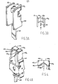
- Each contact has a leg portion extending outwardly from the substrate, a pair of opposing rectangular tongue pieces integrally formed with said leg portion, and abutment portions formed by bending inwardly tip ends of the tongue pieces by an angle more than 90 degrees so that said tip ends come into contact with each other.
- the side ends of the abutment portions are respectively formed with a sloped angle and a bevel angle so that said side ends come into smooth contact with a corresponding one of said IC leads.
- the sloped angle is formed by a vertically running "V"- shaped face, whereas the top portion of the "V"-shaped face has horizontally running bevels.
- FIG. 1 an IC socket which comprises a plastic substrate 13 formed therein with rows of contact embedding holes 11 1 , 11 2 ...11 n and 12 1 , 12 2 ...12 n corresponding in number to IC leads, a moveable plate 19 having projections 16 1 and 16 2 to be inserted into a pair of through-holes 15 1 and 15 2 made in the substrate 13 when engagedly mounted on the substrate, said plate being slidable on the substrate along array lines 17 and 18 of the embedding holes 11 1 , 11 2 ...11 n and 12 1 , 12 2 ...12 n through the turning operation of a handle 14 rotatable provided at a portion of the substrate, said moveable plate being provided with a plurality of insert holes 20 1 , 20 2 ...20 n and 21 1 , 21 2 ,..21 n at positions corresponding to the contact embedding holes 11 1 , 11 2 ...11 n and 12 1 , 12 2 2
- Such contacts 241, 24 2 ... are mounted within respective holes 23 1 , 23 2 ... arranged in a row on a substrate 22, and comprise respective leg portions 25 1 , 25 2 ... extending outwardly from the substrate 22.
- a prior art contact 33 is made by punching a resilient metallic plate and comprises opposing rectangular tongue piece 31 1 and 31 2 and leg portion 32.
- the tongue pieces 31 1 and 31 2 are formed at their upper portions with inwardly directed portions 34 1 and 34 2 raised by a pressing process, and the raised portions are positioned so that the faces of the raised portions come into contact with each other.
- an IC lead 35 is moved in the direction illustrated by arrow 36 by a movement of the moveable plate forcing the lead into the gap between the opposing raised portions 34 1 and 34 2 such that contact is established with the lead.
- the contact pressure of the raised portion often causes the deformation of the lead, resulting in a poor contact between the IC lead and raised portions.
- the major reason is due to the fact that it is difficult to provide the raised portions 341 and 34 2 at or close to the tops of the rectangular tongue pieces 31 1 and 32 2 from the viewpoint of its manufacturing technique and thus the raised portions are provided nearly in the middle of the tongue pieces.
- the IC lead does not come into contact with the contact at the base portion of the IC lead, but rather it is the tip of the lead which comes into contact with the raised portions of the contact, whereby a slight deformation of the lead often causes the shift of the contact position, applying an unnecessary force to the lead and causing the poor contact.
- the contact disadvantageously cannot provide the sufficient and positive contact pressure.
- a contact 41 which includes a leg portion 42 extending outwardly from the substrate, a pair of opposing rectangular tongue pieces 43 1 and 43 2 provided integrally with the leg portion, and abutment portions 44 1 and 44 2 formed by bending inwardly the tip end portions of the tongues by an angle more than 90 degrees and preferably in the range of 100 to 140 degrees so that the tip end portions come into contact with each other close to the top of the contact; and side ends 45 1 and 45 2 of the abutment portions 44 1 and 44 2 are respectively formed with a sloped angle and a bevel angle so that the side ends come into smooth contact with an IC lead 46.
Landscapes
- Engineering & Computer Science (AREA)
- Microelectronics & Electronic Packaging (AREA)
- Connecting Device With Holders (AREA)
Applications Claiming Priority (2)
| Application Number | Priority Date | Filing Date | Title |
|---|---|---|---|
| JP1984016090U JPS60129147U (ja) | 1984-02-09 | 1984-02-09 | 無負荷着脱機構を有するicソケツト |
| JP16090/84 | 1984-02-09 |
Publications (1)
| Publication Number | Publication Date |
|---|---|
| EP0156406A2 true EP0156406A2 (de) | 1985-10-02 |
Family
ID=11906824
Family Applications (1)
| Application Number | Title | Priority Date | Filing Date |
|---|---|---|---|
| EP85200154A Withdrawn EP0156406A2 (de) | 1984-02-09 | 1985-02-08 | IC-Kontaktdose |
Country Status (3)
| Country | Link |
|---|---|
| US (1) | US4647134A (de) |
| EP (1) | EP0156406A2 (de) |
| JP (1) | JPS60129147U (de) |
Families Citing this family (7)
| Publication number | Priority date | Publication date | Assignee | Title |
|---|---|---|---|---|
| US5489217A (en) * | 1994-10-11 | 1996-02-06 | Methode Electronics, Inc. | Zero insertion force pin grid array socket |
| US5597320A (en) * | 1995-01-03 | 1997-01-28 | Molex Incorporated | Zero insertion force electrical connector and terminal |
| US5629837A (en) * | 1995-09-20 | 1997-05-13 | Oz Technologies, Inc. | Button contact for surface mounting an IC device to a circuit board |
| US6046597A (en) * | 1995-10-04 | 2000-04-04 | Oz Technologies, Inc. | Test socket for an IC device |
| JPH11135175A (ja) * | 1997-10-31 | 1999-05-21 | Dai Ichi Denshi Kogyo Kk | ソケットコンタクト及びその製造方法 |
| GB2334631A (en) * | 1998-02-20 | 1999-08-25 | Mitel Semiconductor Ab | Zero insertion force test socket |
| JP3691294B2 (ja) * | 1999-07-30 | 2005-09-07 | ヒロセ電機株式会社 | 電気コネクタ |
Family Cites Families (6)
| Publication number | Priority date | Publication date | Assignee | Title |
|---|---|---|---|---|
| DE1142196B (de) * | 1956-10-31 | 1963-01-10 | Siemens Ag | Kontaktsteckverbindung |
| US3538486A (en) * | 1967-05-25 | 1970-11-03 | Amp Inc | Connector device with clamping contact means |
| US3543217A (en) * | 1968-06-25 | 1970-11-24 | Heyman Mfg Co | Multipurpose electric receptacle fitting and receptacle |
| US3676832A (en) * | 1970-12-28 | 1972-07-11 | Ibm | Connector |
| US4232931A (en) * | 1978-12-19 | 1980-11-11 | Hochiki Corporation | Connector for coaxial cables |
| US4498725A (en) * | 1982-06-02 | 1985-02-12 | Amp Incorporated | Electrical connector |
-
1984
- 1984-02-09 JP JP1984016090U patent/JPS60129147U/ja active Pending
-
1985
- 1985-01-04 US US06/688,646 patent/US4647134A/en not_active Expired - Fee Related
- 1985-02-08 EP EP85200154A patent/EP0156406A2/de not_active Withdrawn
Also Published As
| Publication number | Publication date |
|---|---|
| US4647134A (en) | 1987-03-03 |
| JPS60129147U (ja) | 1985-08-30 |
Similar Documents
| Publication | Publication Date | Title |
|---|---|---|
| US4780603A (en) | Integrated circuit card and connector arrangement using same | |
| EP0295046B1 (de) | Prüfsockel mit verbesserter Kontakteinrastung | |
| EP0233914B1 (de) | An einer oberfläche montierter verbinder | |
| EP0030763B1 (de) | Andruckverbinder für einen integrierten Schaltungsbaustein | |
| KR0159828B1 (ko) | 인쇄 회로 기판용 전기 커넥터 | |
| US5676555A (en) | Card edge connector having means for applying inward transverse force on printed wiring boards | |
| EP0571105B1 (de) | Sockelkontakt | |
| EP0757849B1 (de) | Elektrischer steckverbinder mit oberflächenmontierbaren kontakten | |
| WO2008030657A2 (en) | Electrical connector | |
| JPH02253580A (ja) | 表面実装型電気コネクタ | |
| US6287137B1 (en) | Inspectable electrical connector for a PGA package | |
| US5292265A (en) | Edge mounted circuit board electrical connector | |
| EP0650643A1 (de) | Kartenverbinder mit flacher rückseite | |
| US6139348A (en) | Electric connector with an elastically deformable contact pin | |
| US6908328B2 (en) | Electrical connector with accurately secured contacts | |
| EP0851539A2 (de) | Elektrischer Flachkabelverbinder | |
| US5692920A (en) | Zero insertion force electrical connector and terminal | |
| US4647134A (en) | IC socket contact | |
| US6953350B2 (en) | Straddle electrical connector with two-stage connecting clamp | |
| JPH0349189B2 (de) | ||
| US5707241A (en) | Slide locking connector | |
| US5791929A (en) | Zero insertion force electrical connector and terminal | |
| JPH0668940A (ja) | Fpc接続用コネクタ | |
| EP0299989B1 (de) | Schaltungspaneelbuchse hoher dichte | |
| US5865649A (en) | Card edge connector having means for preventing overstress of contact elements |
Legal Events
| Date | Code | Title | Description |
|---|---|---|---|
| PUAI | Public reference made under article 153(3) epc to a published international application that has entered the european phase |
Free format text: ORIGINAL CODE: 0009012 |
|
| AK | Designated contracting states |
Kind code of ref document: A2 Designated state(s): AT BE CH DE FR GB IT LI LU NL SE |
|
| RBV | Designated contracting states (corrected) |
Designated state(s): DE FR GB |
|
| STAA | Information on the status of an ep patent application or granted ep patent |
Free format text: STATUS: THE APPLICATION HAS BEEN WITHDRAWN |
|
| 18W | Application withdrawn |
Withdrawal date: 19870212 |
|
| RIN1 | Information on inventor provided before grant (corrected) |
Inventor name: NONAKA, YOSHIMASA |