EP0156480B1 - Taktsteuer-Signalgenerator für Teletext-Signalentzerrer - Google Patents
Taktsteuer-Signalgenerator für Teletext-Signalentzerrer Download PDFInfo
- Publication number
- EP0156480B1 EP0156480B1 EP85300952A EP85300952A EP0156480B1 EP 0156480 B1 EP0156480 B1 EP 0156480B1 EP 85300952 A EP85300952 A EP 85300952A EP 85300952 A EP85300952 A EP 85300952A EP 0156480 B1 EP0156480 B1 EP 0156480B1
- Authority
- EP
- European Patent Office
- Prior art keywords
- timing control
- signal
- control signals
- timing
- level
- Prior art date
- Legal status (The legal status is an assumption and is not a legal conclusion. Google has not performed a legal analysis and makes no representation as to the accuracy of the status listed.)
- Expired
Links
- 230000015654 memory Effects 0.000 claims description 29
- 230000008859 change Effects 0.000 claims description 17
- 230000001360 synchronised effect Effects 0.000 claims description 7
- 230000004044 response Effects 0.000 claims description 3
- 238000010586 diagram Methods 0.000 description 6
- 238000000034 method Methods 0.000 description 4
- 230000008569 process Effects 0.000 description 4
- 239000000284 extract Substances 0.000 description 2
- 229910002056 binary alloy Inorganic materials 0.000 description 1
- 230000005540 biological transmission Effects 0.000 description 1
- 238000010276 construction Methods 0.000 description 1
- 230000006872 improvement Effects 0.000 description 1
- 238000005259 measurement Methods 0.000 description 1
- 230000004048 modification Effects 0.000 description 1
- 238000012986 modification Methods 0.000 description 1
- 230000008707 rearrangement Effects 0.000 description 1
- 230000000630 rising effect Effects 0.000 description 1
- 238000005070 sampling Methods 0.000 description 1
Images


Classifications
-
- H—ELECTRICITY
- H04—ELECTRIC COMMUNICATION TECHNIQUE
- H04N—PICTORIAL COMMUNICATION, e.g. TELEVISION
- H04N21/00—Selective content distribution, e.g. interactive television or video on demand [VOD]
- H04N21/40—Client devices specifically adapted for the reception of or interaction with content, e.g. set-top-box [STB]; Operations thereof
- H04N21/47—End-user applications
- H04N21/488—Data services, e.g. news ticker
- H04N21/4888—Data services, e.g. news ticker for displaying teletext characters
-
- H—ELECTRICITY
- H04—ELECTRIC COMMUNICATION TECHNIQUE
- H04N—PICTORIAL COMMUNICATION, e.g. TELEVISION
- H04N21/00—Selective content distribution, e.g. interactive television or video on demand [VOD]
- H04N21/40—Client devices specifically adapted for the reception of or interaction with content, e.g. set-top-box [STB]; Operations thereof
- H04N21/47—End-user applications
-
- H—ELECTRICITY
- H04—ELECTRIC COMMUNICATION TECHNIQUE
- H04N—PICTORIAL COMMUNICATION, e.g. TELEVISION
- H04N7/00—Television systems
- H04N7/025—Systems for the transmission of digital non-picture data, e.g. of text during the active part of a television frame
- H04N7/035—Circuits for the digital non-picture data signal, e.g. for slicing of the data signal, for regeneration of the data-clock signal, for error detection or correction of the data signal
-
- H—ELECTRICITY
- H04—ELECTRIC COMMUNICATION TECHNIQUE
- H04N—PICTORIAL COMMUNICATION, e.g. TELEVISION
- H04N5/00—Details of television systems
- H04N5/44—Receiver circuitry for the reception of television signals according to analogue transmission standards
- H04N5/445—Receiver circuitry for the reception of television signals according to analogue transmission standards for displaying additional information
- H04N5/44504—Circuit details of the additional information generator, e.g. details of the character or graphics signal generator, overlay mixing circuits
Definitions
- the present invention relates to a waveform equalizer for a Teletext signal and, more particularly, to an improvement in an operation timing control signal generator for use in this waveform equalizer.
- Teletext services whereby textual and graphic information is inserted into television broadcast signals and this teletext signal is converted to a television signal in a TV receiver to be displayed on the screen.
- the Teletext signal is inserted, in the form of a two-level signal and, subsequent to a color burst signal, into one or more horizontal scanning lines in the vertical blanking interval of the television signal.
- a data packet of the Teletext signal consists of a header and information data. According to the system in Japan, the data packet has 320 samples and the sampling clock rate is 5.73 mega samples/second.
- waveform equalizer waveform equalizer
- the video signal has to be processed on a real-time basis to remove ghost components.
- the ghost canceller has to be designed so as to operate at high speed, which has led them to be large in circuit scale and costly. It is economically disadvantageous to use such a picture ghost canceller to remove the ghost components from the Teletext signal having a frequency band narrower than the video signal. Further, since the above picture ghost cancellers cannot eliminate short-delay ghosts, they cannot be adapted for a Teletext signal equalizer without modification.
- the Teletext signal is transmitted within the vertical blanking interval of the television signal, the real-time process is not always necessary to eliminate the waveform distortions. That is, the waveform equalizing process can be performed during a video signal interval (one field interval). This means that an equalizer which may be simple in arrangement and operate at low speed is enough for equalization of the waveform of the Teletext signal.
- An example of the waveform equalizer for the Teletext signal is disclosed in Japanese Laid-Open Patent Publication No. 56 (1981)-166674 (JP-A-58/66 846, Pub. Date 21.04.1983).
- timing control signals are needed to determine the operation timings of circuits. Further, for the waveform equalizing process, about 90,000 shots of 5.73 MHz clock pulses are needed in one field interval (about 16 milliseconds). A low-speed microprocessor is not adapted for generating such high-speed timing signals.
- a conventional timing control signal generator mainly consists of TTL logic ICs including counters, flip-flops and the like. However, in this case, the number of elements constituting the counters increases, causing the circuit scale to be remarkably enlarged. Actually, about 300 general-purpose logic ICs are used.
- a timing control signal generator comprises a synchronous circuit means connected to receive a television signal for generating a field start signal indicative of the start of a vertical blanking interval and sample clock pulses which have a frequency equal to the sample clock rate of a Teletext signal and are phase-locked with samples of the Teletext signal; first and second counter means; and first and second read only memories (ROMs).
- ROMs read only memories
- the first ROM stores the respective level information of the timing control signals at respective level change timings of the timing control signals, while the second ROM stores information as to a time duration between each level change timing and the next level change timing of a predetermined timing control signal.
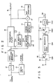
- a television signal demodulated by a demodulator (not shown) is applied through an input terminal 11 to an analog-to-digital (A/D) converter 12 and a timing signal generating circuit 13.
- the television signal is converted to a 6-bit digital form by the A/D converter 12.
- a digital output signal of the A/D converter 12 is applied to an input waveform memory 14, which extracts a Teletext signal in response to the timing signal generator 13 and stores the waveform of the Teletext signal in a digital form.
- the A/D converter 12 may be constituted so as to convert only the Teletext signal to a digital signal.
- the A/D converter 12 converts each sample of the two-level Teletext signal to six-bit digital data including a sign bit. As will be easily understood, in the case where the Teletext signal is subjected to waveform distortions due to ghost components, the amplitude of each sample varies depending upon the magnitude of ghost . components.
- the Teletext signal waveform read out from the input waveform memory 14 is applied to a transversal filter 15 for waveform equalization.
- An output signal of the transversal filter 15 is sent to a utilization circuit (not shown) through an output terminal 16, and to a subtracter 17 and a reference waveform generator 18.
- the reference waveform generator 18 examines the sign of a digital output signal of the transversal filter 15 and applies an output signal to the subtracter 17.
- the output signal of the reference waveform generator 18 is +1 when the sign is plus and -1 when it is minus.
- the subtracter 17 calculates the difference between the output signals of the transversal filter 15 and reference waveform generator 18, thereby producing data indicative of an error in the waveform.
- the error waveform data is stored in an error waveform memory 19.
- the error waveform data from the error waveform memory 19 and the Teletext signal waveform from the input waveform memory 14 are applied to a tap weight computing circuit 20, which computes the correlation between the input waveform and the error waveform to obtain optimum tap weights of the transversal filter 15.
- the tap weights are stored in a tap weight memory 21, thereby applying tap weight data to the transversal filter 15.
- the number of taps of the transversal filter 15 is 24.
- the error waveform computation, tap weight computation and convolution computation in the transversal filter 15 may be performed within one field interval of the television signal.
- the operation of the Teletext signal waveform equalizer is governed by a clock signal CK (5.73 MHz) in the case of the Teletext system in Japan) and various kinds of timing control signals from the timing signal generator 13.
- the input waveform memory 14 is comprised of a shift register with 324 stages each connected to receive a word of 6-bits in parallel as shown in Fig. 3.
- the shift register is divided into a 300-stage shift register 33 and a 24-stage shift register 35.
- a switching circuit 32 is connected between an input terminal 31 and the shift register 35, while a switching circuit 34 is connected between the shift registers 33 and 35.
- Each of the electronic-type switching circuits 32 and 34 is of a single-pole double-throw type having stationary contacts A and B. The contacts A and B of the switching circuit 32 are connected to the input terminal 31 and the output of shift register 35, respectively.
- the contacts A and B of the switching circuits 34 are connected to outputs of the shift registers 33 and 35, respectively.
- the electronic switching circuits 32 and 34 are controlled by the operation of timing control signals SW1 and SW2 respectively, which are generated from the timing signal generator 13.
- Clock signals CK1 and CK2 of 5.73 MHz from the timing signal generator 13 are supplied to the shift registers 33 and 35, respectively, so that digital data is shifted right in the shift registers 33 and 35.
- the number of stages of the shift register 35 is equal to the number of taps of the transversal filter 15.
- 0 denotes that the clock signal is supplied to the corresponding shift register and X means that no clock signal is supplied.
- the timing signal generator 13 receives the TV signal to generate a field start signal FSTRT indicative of the start of a field, the sample clock signals CK, CK1 and CK2 phase-locked to the color burst signal, and various operation timing control signals including SW1 and SW2.
- the sample clock frequency (5.73 MHz) is set at 8/5 times the color burst signal frequency (3.58 MHz) of the NTSC color television system.
- the timing signal generator 13 detects a vertical blanking interval of a TV signal to generate the field start signal FSTRT.
- the switching circuits 32 and 34 are switched to the side B by the timing control signals SW1 and SW2, respectively. This occurs from the start of the field until the beginning of the Teletext signal, which allows the shift registers 33 and 35 to be disconnected from the A/D converter 12.
- the switching circuits 32 and 34 are switched to the side A by the timing control signals SW1 and SW2, respectively, thereby permitting the digital Teletext signal to be loaded into the shift registers 33 and 35.
- the switching circuits 32 and 34 are changed over to the side B by the control signals SW1 and SW2 and thereafter an error waveform operation mode EW is started.
- the error waveform operation is executed 48 times for every 24 samples.
- the clock pulse CK1 is not generated but 24 clock pulses CK2 are generated.
- the data in the shift register 35 recirculates while being loaded into the transversal filter 15.
- the switching circuit 34 is switched to the side A, for only one clock pulse interval, by the switch control signal SW2 while the switching circuit 32 remains switched to the side B.
- the shift registers 33 and 35 serve as a circulating shift register for the interval EW1-@ so that the data is shifted one stage right.
- the convolution is computed in accordance with the 24 sample data loaded in the transversal filter 15 and the tap weight coefficients from the tap weight memory 26.
- the result of the computation is applied to the subtracter 17 to produce an error waveform component which is stored in the error waveform memory 19.
- the data is read out 48 times on a 24-sample data unit basis from the input waveform memory 14, so that the convolution computation is executed 48 times and the data necessary for the gain computation for 24 taps of the transversal filter 15 is stored in the error waveform memory 19.
- the rearrangement mode is executed to rearrange data in the shift registers 33 and 35 in the original input sequence.
- the switching circuit 32 is switched to the side B and the switching circuit 34 is switched to the side A. 276 clock pulses CK1 and CK2 are applied to the shift registers 33 and 35, respectively, and 324 sample data are rearranged in the original input sequence.
- the processes of tap-weight computing in the tap weight computing circuit 20, writing the computed tap weight into the tap gain memory 21, and correcting the tap weights of the transversal filter 15 are executed.
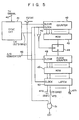
- a video signal is applied, through an inputterminal 40, to a synchronous circuit 41 which detects a vertical sync signal and extracts a color burst signal.
- the synchronous circuit 41 produces the field start signal FSTRT and the sample clock signal CK of 5.73 MHz.
- the field start signal FSTRT is applied to clear terminals of first and second counters 42 and 48, thereby initializing these counters every field.
- the sample clock signal CK is applied to the A/D converter 12 through a terminal 46 and to clock terminals of the counter 42 and a latch circuit 50.
- the counter 42 is a binary counter having bit outputs which is responsive to the rising edge of the sample clock signal CK to vary output state in accordance with the binary system. Outputs of the counter 42 are coupled to address inputs of a first read only memory (ROM) 43.
- ROM read only memory
- Binary data indicative of the changing points, occurring after the start of the field, of the operation timing control signals such as SW1 and SW2 has been stored in the ROM 43.
- Data of 1 is stored in addresses of the ROM 43 which correspond to times at which the level of at least one of the timing control signals including SW1 and SW2 changes after the start of the field, while data of 0 is stored in other addresses thereof.
- the addresses of the ROM 43 are designated by the counter 42 for measuring time from the start of the field on the basis of the sample clock signal CK. Therefore, data of 1 is read out from the ROM 43 whenever times, at which the level of the timing control signal should vary (these times have been predetermined), elapse with reference to the start time of the field.
- An output signal of the ROM 43 is latched in a flip-flop 44 responsive to an inverted sample clock signal from an inverter 45, thereby driving the second counter 48.
- the counter 48 is a binary counter like the first counter 43, which counts 1 data outputs of the ROM 43, i.e., changing points of the timing control signal, thereby accessing a second ROM 49.
- the ROM 49 has, for instance, eight outputs corresponding to the number of necessary timing control signals for one address. ROM 49 stores, in each address thereof (corresponding to one changing point of the timing control signals) designated by counter 48, the level information (1 or 0) of each timing control signal at each changing point of the timing control signals. Consequently, eight data representative of the levels of eight timing control signals are read out from the ROM 49 at every changing point of the- timing control signals.
- Timing control signals T1 to T8 are taken from output terminals 47a to 47h of the latch circuit 50.
- the control signals SW1 and SW2 as shown in Fig. 4 are taken from the output terminals T1 and T2.
- the timing control signals for the Teletext signal waveform equalizer which have little regularity and must vary at a speed of 5.73 MHz, can be generated on a relatively small circuit scale.
- the timing control signal generator may be sufficiently constituted by 10 to 20 general-purpose ICs.
- an eight-bit low-speed ROM is used as the first ROM.
- the sample clock signal CK is applied to a three-bit binary counter 57 so that its frequency is divided by 8.
- the MSB output of the counter 57 is applied to the clock input of the first counter 42.
- Outputs of the first counter 42 designate addresses of the first ROM 43.
- the MSB output of the counter 57 is inverted by an inverter 54 and then applied to a clock input of a latch circuit 55.
- the latch circuit 55 latches output data of the ROM 43 at the falling edge of the MSB output of the counter 57.
- a selector 56 sequentially selects one of eight outputs of the ROM 43 in response to three-bit outputs of the counter 57 and sends it to the flip flop 44 in Fig. 5. Thereafter, various timing control signals are produced in a similar manner as in the case of Fig. 5.
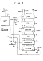
- a synchronous circuit 61 receives a video signal through an input terminal 60 to produce the field start signal FSTRT and sample clock signal CK.
- the field start signal FSTRT is applied to clear terminals of first and second counters 62 and 63.
- the sample clock signal CK is applied to a clock terminal of the counter 62 through an AND gate 64.
- the AND gate 64 is enabled by the Q output of a flip-flop 65. As will be described later, the AND gate 64 is enabled by the flip-flop 65 when at least one of the timing control signals changes. Therefore, the counter 62 counts one shot of sample clock signal CK when the level of at least one of the timing control signals changes after the counter 62 has been cleared by the field start signal FSTRT.
- Outputs of the counter 62 are coupled to address inputs of first and second ROMs 66 and 67.
- the ROM 66 stores in each address the level data of 8 timing control signals at each change point thereof.
- the data read out from the ROM 66 is latched in a latch circuit 68 responsive to the sample clock CK from the AND gate 64.
- the latch circuit 68 holds data read out from the ROM 66 at the previous change point until the next change occurs in the timing control signals.
- Eight timing control signals are generated from eight outputs 68a to 68h of the latch circuit 68 in a similar manner as the foregoing embodiment.
- the ROM 67 stores data as to the respective time durations of the 1-level intervals and 0-level intervals of one timing control signal, in other words, data as to time duration between adjacent change points of this timing control signal.
- the counter 63 is cleared through an OR gate 69 by the field start signal FSTRT or the Q output of the flip-flop 65.
- the counter 63 counts the sample clock signal CK to measure time running from a changing point of the timing control signal indicated by the Q output of the flip-flop 65.
- the outputs of the ROM 67 and counter 63 are compared by a comparator 70. When both outputs coincide, the comparator 70 sends a 1 output to the D input of the flip-flop 65.
- the inverted signal of the sample clock CK is applied through an inverter 71 to the clock terminal of the flip-flop 65.
- the flip-flop 65 holds the 1 output of the comparator 70 at the falling edge of the sample clock CK.
- the AND gate 64 is enabled to cause the counter 62 to count one sample clock CK, and at the same time the counter 63 is cleared, thereby allowing the measurement of time to be restarted. In this way, the timing control signals, necessary for the waveform equalization, are generated.
- capacities of ROMs may be smaller than those in the case of Fig. 5.
Landscapes
- Engineering & Computer Science (AREA)
- Multimedia (AREA)
- Signal Processing (AREA)
- Television Systems (AREA)
- Picture Signal Circuits (AREA)
- Cable Transmission Systems, Equalization Of Radio And Reduction Of Echo (AREA)
Claims (3)
Applications Claiming Priority (2)
| Application Number | Priority Date | Filing Date | Title |
|---|---|---|---|
| JP59025974A JPS60171833A (ja) | 1984-02-16 | 1984-02-16 | 文字信号用波形等化器 |
| JP25974/84 | 1984-02-16 |
Publications (2)
| Publication Number | Publication Date |
|---|---|
| EP0156480A1 EP0156480A1 (de) | 1985-10-02 |
| EP0156480B1 true EP0156480B1 (de) | 1988-04-20 |
Family
ID=12180697
Family Applications (1)
| Application Number | Title | Priority Date | Filing Date |
|---|---|---|---|
| EP85300952A Expired EP0156480B1 (de) | 1984-02-16 | 1985-02-13 | Taktsteuer-Signalgenerator für Teletext-Signalentzerrer |
Country Status (3)
| Country | Link |
|---|---|
| US (1) | US4625241A (de) |
| EP (1) | EP0156480B1 (de) |
| JP (1) | JPS60171833A (de) |
Families Citing this family (12)
| Publication number | Priority date | Publication date | Assignee | Title |
|---|---|---|---|---|
| DE3751410T2 (de) * | 1986-04-18 | 1996-04-11 | Nagra Plus Sa | Decoder für ein Fernsehgebührensystem. |
| US5220426A (en) * | 1988-02-05 | 1993-06-15 | Karlock James A | Circuitry for removing information from, or modifying information in, the vertical interval of a television signal |
| US4870297A (en) * | 1988-02-05 | 1989-09-26 | Karlock James A | Circuitry for removing information from, or modifying information in, the vertical interval of a television signal |
| DE3809075A1 (de) * | 1988-03-18 | 1989-09-28 | Philips Patentverwaltung | Steuersignalgenerator fuer die verarbeitung eines videosignales |
| CA1305788C (en) * | 1988-03-22 | 1992-07-28 | Tatsuya Shiki | Ghost canceling apparatus |
| JP2594639B2 (ja) * | 1989-03-23 | 1997-03-26 | 株式会社日立製作所 | テレビジョン映像受信信号波形歪み検出方法並びにそれに使用するテレビジョン映像信号送信装置および受信装置 |
| DE4343951A1 (de) * | 1993-12-22 | 1995-06-29 | Inst Rundfunktechnik Gmbh | Verfahren zum Empfangen von in einem Fernsehsignal übertragenen Teletextdaten |
| DE19741434C2 (de) * | 1997-09-19 | 1999-07-08 | Siemens Ag | Abtrennstufe zum Abtrennen eines Signals, das in Austastlücken eines Videosignals übertragen wird und Entzerrungsverfahren für ein solches Signal |
| DE60139253D1 (de) * | 2000-05-22 | 2009-08-27 | Panasonic Corp | Chipkarte |
| US6806910B2 (en) * | 2001-01-04 | 2004-10-19 | Zoran Microelectronics Ltd. | Processing multiple streams of data encoded in respective VBI channels with a shared equalizer |
| JP3771223B2 (ja) * | 2003-02-26 | 2006-04-26 | ローム株式会社 | タイミング調整装置 |
| US7332936B2 (en) * | 2004-12-03 | 2008-02-19 | Semiconductor Energy Laboratory Co., Ltd. | Semiconductor circuit, display device, electronic apparatus |
Family Cites Families (2)
| Publication number | Priority date | Publication date | Assignee | Title |
|---|---|---|---|---|
| US4202012A (en) * | 1977-03-15 | 1980-05-06 | Matsushita Electric Industrial Co., Ltd. | Sampling clock reproducing device |
| JPS55109023A (en) * | 1979-02-14 | 1980-08-21 | Toshiba Corp | Automatic equalizer |
-
1984
- 1984-02-16 JP JP59025974A patent/JPS60171833A/ja active Pending
-
1985
- 1985-02-13 EP EP85300952A patent/EP0156480B1/de not_active Expired
- 1985-02-14 US US06/701,515 patent/US4625241A/en not_active Expired - Lifetime
Also Published As
| Publication number | Publication date |
|---|---|
| US4625241A (en) | 1986-11-25 |
| EP0156480A1 (de) | 1985-10-02 |
| JPS60171833A (ja) | 1985-09-05 |
Similar Documents
| Publication | Publication Date | Title |
|---|---|---|
| US4625241A (en) | Timing control signal generator for teletext signal waveform equalizer | |
| KR900006472B1 (ko) | 샘플링 클록 재생회로 | |
| US4673983A (en) | Picture-in-picture television receivers | |
| EP0469647B1 (de) | Entscheidungsrückgekoppelter Dekodierer mit Pipeline-Struktur | |
| US4404600A (en) | Ghost signal cancelling apparatus | |
| US6480239B1 (en) | Ghost cancellation reference signal with bessel chirps and PN sequences, and TV receiver using such signal | |
| JPH0834598B2 (ja) | 信号遷移強調装置 | |
| US7133481B2 (en) | Synchronization detection apparatus | |
| KR920003719B1 (ko) | 디코더용 등화기 | |
| JP2000506716A (ja) | 同一チャネル干渉を受けるdtv信号用受信機のチャネル等化器の動作方法 | |
| CA1154102A (en) | Intelligent teletext decoder | |
| EP0187540B1 (de) | Schaltung zur Geräuschunterdrückung für Videosignale | |
| JP2000244777A (ja) | 波形等化装置 | |
| GB2174567A (en) | Deriving frame interval signals | |
| EP0056052B1 (de) | Synchronisierender kreis, anpassbar an verschiedene fernsehsysteme | |
| GB2063627A (en) | Arrangement for determining a data slicing level for a bi-amplitude data pulse signal | |
| US4651212A (en) | Signal offset circuitry for digital deghosting system | |
| US5194832A (en) | Transversal equalizer | |
| JPS6259950B2 (de) | ||
| SU1672587A1 (ru) | Устройство коррекции искажений сигнала телевизионного изображени | |
| KR0170637B1 (ko) | 디2-멀티 아날로그 콤포넌트 디코더 집적회로 | |
| KR20030065177A (ko) | 디스플레이 장치의 샤프니스 보정장치 | |
| KR0139158B1 (ko) | 고스트제거기준(gcr)신호검출방법 및 그 장치 | |
| JPH0518308B2 (de) | ||
| KR950001506B1 (ko) | 자동 위상 등화 장치 |
Legal Events
| Date | Code | Title | Description |
|---|---|---|---|
| PUAI | Public reference made under article 153(3) epc to a published international application that has entered the european phase |
Free format text: ORIGINAL CODE: 0009012 |
|
| 17P | Request for examination filed |
Effective date: 19850222 |
|
| AK | Designated contracting states |
Designated state(s): DE FR GB NL |
|
| 17Q | First examination report despatched |
Effective date: 19870518 |
|
| RBV | Designated contracting states (corrected) |
Designated state(s): FR GB |
|
| GRAA | (expected) grant |
Free format text: ORIGINAL CODE: 0009210 |
|
| AK | Designated contracting states |
Kind code of ref document: B1 Designated state(s): FR GB |
|
| ET | Fr: translation filed | ||
| PLBE | No opposition filed within time limit |
Free format text: ORIGINAL CODE: 0009261 |
|
| STAA | Information on the status of an ep patent application or granted ep patent |
Free format text: STATUS: NO OPPOSITION FILED WITHIN TIME LIMIT |
|
| 26N | No opposition filed | ||
| REG | Reference to a national code |
Ref country code: GB Ref legal event code: 746 Effective date: 19981007 |
|
| REG | Reference to a national code |
Ref country code: FR Ref legal event code: D6 |
|
| PGFP | Annual fee paid to national office [announced via postgrant information from national office to epo] |
Ref country code: GB Payment date: 20000209 Year of fee payment: 16 |
|
| PGFP | Annual fee paid to national office [announced via postgrant information from national office to epo] |
Ref country code: FR Payment date: 20000210 Year of fee payment: 16 |
|
| PG25 | Lapsed in a contracting state [announced via postgrant information from national office to epo] |
Ref country code: GB Free format text: LAPSE BECAUSE OF NON-PAYMENT OF DUE FEES Effective date: 20010213 |
|
| GBPC | Gb: european patent ceased through non-payment of renewal fee |
Effective date: 20010213 |
|
| PG25 | Lapsed in a contracting state [announced via postgrant information from national office to epo] |
Ref country code: FR Free format text: LAPSE BECAUSE OF NON-PAYMENT OF DUE FEES Effective date: 20011031 |
|
| REG | Reference to a national code |
Ref country code: FR Ref legal event code: ST |