EP0157207A2 - Thyristor à commande d'extinction - Google Patents
Thyristor à commande d'extinction Download PDFInfo
- Publication number
- EP0157207A2 EP0157207A2 EP85102520A EP85102520A EP0157207A2 EP 0157207 A2 EP0157207 A2 EP 0157207A2 EP 85102520 A EP85102520 A EP 85102520A EP 85102520 A EP85102520 A EP 85102520A EP 0157207 A2 EP0157207 A2 EP 0157207A2
- Authority
- EP
- European Patent Office
- Prior art keywords
- layer
- thyristor
- conductivity type
- substrate
- gate turn
- Prior art date
- Legal status (The legal status is an assumption and is not a legal conclusion. Google has not performed a legal analysis and makes no representation as to the accuracy of the status listed.)
- Ceased
Links
Images

Classifications
-
- H—ELECTRICITY
- H10—SEMICONDUCTOR DEVICES; ELECTRIC SOLID-STATE DEVICES NOT OTHERWISE PROVIDED FOR
- H10D—INORGANIC ELECTRIC SEMICONDUCTOR DEVICES
- H10D62/00—Semiconductor bodies, or regions thereof, of devices having potential barriers
- H10D62/10—Shapes, relative sizes or dispositions of the regions of the semiconductor bodies; Shapes of the semiconductor bodies
- H10D62/102—Constructional design considerations for preventing surface leakage or controlling electric field concentration
- H10D62/103—Constructional design considerations for preventing surface leakage or controlling electric field concentration for increasing or controlling the breakdown voltage of reverse-biased devices
- H10D62/104—Constructional design considerations for preventing surface leakage or controlling electric field concentration for increasing or controlling the breakdown voltage of reverse-biased devices having particular shapes of the bodies at or near reverse-biased junctions, e.g. having bevels or moats
-
- H—ELECTRICITY
- H10—SEMICONDUCTOR DEVICES; ELECTRIC SOLID-STATE DEVICES NOT OTHERWISE PROVIDED FOR
- H10D—INORGANIC ELECTRIC SEMICONDUCTOR DEVICES
- H10D18/00—Thyristors
- H10D18/60—Gate-turn-off devices
-
- H—ELECTRICITY
- H10—SEMICONDUCTOR DEVICES; ELECTRIC SOLID-STATE DEVICES NOT OTHERWISE PROVIDED FOR
- H10D—INORGANIC ELECTRIC SEMICONDUCTOR DEVICES
- H10D62/00—Semiconductor bodies, or regions thereof, of devices having potential barriers
- H10D62/10—Shapes, relative sizes or dispositions of the regions of the semiconductor bodies; Shapes of the semiconductor bodies
- H10D62/13—Semiconductor regions connected to electrodes carrying current to be rectified, amplified or switched, e.g. source or drain regions
- H10D62/141—Anode or cathode regions of thyristors; Collector or emitter regions of gated bipolar-mode devices, e.g. of IGBTs
- H10D62/142—Anode regions of thyristors or collector regions of gated bipolar-mode devices
-
- H—ELECTRICITY
- H10—SEMICONDUCTOR DEVICES; ELECTRIC SOLID-STATE DEVICES NOT OTHERWISE PROVIDED FOR
- H10D—INORGANIC ELECTRIC SEMICONDUCTOR DEVICES
- H10D62/00—Semiconductor bodies, or regions thereof, of devices having potential barriers
- H10D62/60—Impurity distributions or concentrations
Definitions
- the present invention relates to a gate turn-off thyristor, and more particularly, to a gate turn-off thyristor which is improved in its current cut-off performance by minimizing the current amplification factor of one of the transistor elements in the thyristor structure.
- the gate turn-off thyristor (referred to as simply a "GTO" thyristor, hereinafter) is a thyristor which is capable of cutting off current by a gate control in which current is drawn out from the gate and is therefore put into practical use in, for example, an inverter device for controlling the speed of a motor.
- the turn-off gain G o f f (i.e. the ratio between the on-state current flowing when the thyristor is conductive and the gate turn-off current required for cutting off the current) of the thyristor is, as is well known, given by the following formula:
- a 32 represents the current amplification factor of one of the transistor elements in the thyristor structure which has a gate control terminal connected to its base, while a 12 represents the current amplification factor of the other transistor element of the thyristor structure.
- a P base type thyristor which is more general, will be described hereinafter, and the current amplification factors a 32 and ⁇ 12 will be respectively referred to as "a(n-p-n): and "a(p-n-p)".
- the first method features doping with a heavy metal, such as gold. Doping with a heavy metal is done with the intent of reducing the carrier life in the N B layer and thereby decreasing the coefficient of transportation of carriers to the base and, as a result, the current amplification factor a(p-n-p) is minimized.
- a heavy metal such as gold
- the second method of minimizing the current amplification factor a(p-n-p) features shunting the P emitter.
- This structure is equivalent to a structure in which the emitter and base of a p-n-p transistor are shunted to each other through a resistor. It is intended by the equivalent shunt resistor to reduce the effective emitter injection efficiency in the p-n-p transistor, thereby minimizing the current amplification factor a(p-n-p).
- the heavy-metal doping method advantageously makes it possible to improve the current cut-off performance of a thyristor element without impairing its fundamental functional aspect as a thyristor.
- the heavy-metal doping method is disadvantageous in that a relatively short carrier lifetime in the N B layer involves increases in the on-state voltage and the leakage current and in that doping with a heavy metal may cause various problems at high temperature including a lowering in the performance of the thyristor element.
- the second method in which the P emitter is short-circuited advantageously makes it possible to overcome the disadvantage of the first method since it is possible to maintain the carrier lifetime at a high level.
- the second method involves a disadvantage in that the thyristor loses the function of blocking the reverse voltage since the P E layer is shunted by the N +- type layers.
- the GTO thyristor was mainly applied to a voltage-type inverter device. In this device, only a forward voltage is applied to a thyristor element therein, that is, no reverse voltage is applied to the thyristor element. Therefore, early GTO thyristors did not need the capability of blocking a reverse voltage.
- the thyristor has been applied to devices other than the voltage type inverter, such as a current type inverter, converter and chopper. In these devices, a reverse voltage equal in magnitude to a forward voltage is applied to a thyristor element.
- a primary object of the present invention is to realize a GTO thyristor of high current cut-off performance by overcoming the respective disadvantages of the above-described conventional methods, that is, by preventing the occurrence of any lowering in various other characteristics, while, at the same time, maintaining the function of blocking the reverse voltage.
- a gate turn-off thyristor which includes a semiconductor substrate having a first layer which is exposed on one of its main surfaces and is of a first conductivity type, a second layer which is adjacent to the first layer and is of a second conductivity type, a third layer which is adjacent to the second layer and is exposed on the other main surface of the substrate, said third layer being of the-first conductivity type, a fourth layer which is adjacent to the third layer and is exposed on the main surface of the substrate, said fourth layer being of the second conductivity type, and a fifth layer which is provided between the first layer and the second layer and which is of the first conductivity type.
- the fifth layer has an impurity concentration which is selected to be smaller than that in said second layer.
- the structure includes PN junctions formed respectively between adjacent ones of said layers which are different from each other in conductivity type.
- a first main electrode is conductively connected to at least the first layer
- a second main electrode is conductively connected to the fourth layer
- a gate electrode is connected to the third layer.
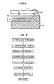
- thyristors generally include a P emitter (a P E layer) connected to an anode electrode A, and an N base (an N B layer) adjacent to the P emitter.
- a P base (a P B layer) adjacent to the N base (an N B layer) is also generally connected to a gate electrode G.
- an N emitter (an N E layer) adjacent to the P base is typically connected to a cathode electrode K.
- the P E layer adjacent to the N B layer is provided with a P-type layer of low impurity concentration (referred to as a " ⁇ layer”, hereinafter) interposed between the F E layer and the N B layer.
- ⁇ layer P-type layer of low impurity concentration
- Fig. 1B shows an impurity concentration profile for the structure of Fig. lA.
- the distance x on the abscissa corresponds to the same dimension shown in Fig. lA.
- the ordinate represents impurity concentration (i.e., the number of impurity atoms per cm 3 ).
- the impurity concentration in the ⁇ layer is set such as to be lower than that in the N B layer, that is, about one-tenth of that in the N B layer. For example, when the impurity concentration in the N B layer is 5 x 10 14 atom/cm 3 , the impurity concentration in the ⁇ layer is set to 5 x I0 13 ato m/cm 3 .
- the injection efficiency y at a PN junction is represented by the following formula:
- the injection efficiency y is substantially equal to 1.
- the injection efficiency y is equal to 0.5.
- the injection efficiency y is substantially equal to 0.
- the provisions of the ⁇ layer of low impurity concentration on the side of the P E layer on which it is in contact with the N B layer as in the case of the present invention makes it possible to minimize the injection efficiency at the PN junction concerned.
- the structure of the present invention is regarded as an arrangement in which the emitter and base of a p-n-p transistor are shunted to each other through a capacitance C, as shown by an equivalent circuit of Fig. 1C.
- the GTO thyristor When the GTO thyristor is turned ON, the anode current is by-passed through the capacitance C to charge the same, whereby it is possible to lower the current amplification factor a(p-n-p) effectively.
- the GTO thyristor When the GTO thyristor is turned OFF, the p-n-p transistor can be quickly turned OFF by the discharge current from the capacitance C.
- Fig. 2A is a schematic illustration for describing the turn-on operation of the GTO thyristor in accordance with the present invention.
- the impurity concentration in the ⁇ layer is lower than that in the N B layer, it is possible to substantially prevent the injection of holes into the N B layer from the ⁇ layer.
- the holes injected from the P E layer as shown by the arrow 10 are employed to increase the carrier concentration in the r layer.
- the hole concentration in the ⁇ layer is rapidly increased to exceed the electron concentration in the N B layer.
- the injection of holes into the N B layer occurs, causing the GTO thyristor to turn ON.
- the anode current flows as shown by the arrow 11.
- the ⁇ layer is filled up with the holes injected from the P E layer and therefore operates as an emitter which excellently injects the holes into the N B layer.
- Fig. 2B is a schematic illustration for describing the turn-off operation of the thyristor in accordance with the present invention.
- the gate turn-off current 21 sweeps the excess carriers in the P B layer and draws in the anode current to the gate G as shown by the arrow 22.
- the holes injected into the N B layer from the 7 layer return back to the 7 layer as shown by the arrow 23 due to a rapid reduction in the amount of excess carriers in the ⁇ layer and, therefore, the excess carriers in the N B layer are rapidly swept out.
- the turn-off ability of the thyristcr element is improved by the above-described mechanism.
- the GTO thyristor in accordance with the present invention has the function of blocking the reverse voltage. This is because the ⁇ -N B junction formed all over one surface of the N B layer has an excellent voltage-blocking performance and because the junction is not exposed such as to shunt to the anode electrode.
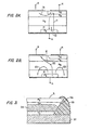
- Figs. 3 and 4 are schematic sectional views respectively showing the structure of an end surface passivation of a conventional GTO thyristor and that of the GTO thyristor in accordance with the present invention.
- Fig. 3 shows the end surface structure of a conventional GTO thyristor showing a GTO thyristor element 31, an anode electrode 32 and a protective element 33 (e.g., passivation glass) and having a reverse-voltage blocking characteristic.
- a GTO thyristor element 31 an anode electrode 32 and a protective element 33 (e.g., passivation glass) and having a reverse-voltage blocking characteristic.
- machining known as "bevelling”.
- the end surface 31A of the GTO thyristor element 31 is machined such that the sectional area of the portion of the thyristor on the side thereof which is closer to the N B layer of low impurity concentration is smaller than that of the portion of the thyristor on the other side thereof.
- Fig. 4 shows one example of the end surface structure of the GTO thyristor in accordance with the invention. It shows a GTO thyristor element 41, an anode electrode 42 and a protective layer 43.
- the depletion layer 44 (the shaded portion in the figure) is satisfactorily expanded, thus preventing any lowering of the reverse-voltage blocking characteristic.
- the GTO thyristor in accordance with the present invention a single bevelling allows both the forward blocking junction and the reverse blocking junction to have positive bevelling and, therefore, it is easy to improve the voltage blocking characteristic.
- the anode electrode 42 may be provided only on the P E layer as in the case of this embodiment. From the viewpoint of minimization of the current amplification factor a(p-n-p), however, it is preferable that the anode electrode 42 should also be provided on the ⁇ layer as shown in Fig. lA.
- the GTO thyristor in accordance with the present invention is improved in its current cut-off characteristic by the above-described operational function of the ⁇ -N B junction. Therefore, as will be clear from this fact, there is no need for doping with a heavy metal, such as gold.
- Fig. 5 is a flowchart showing one example of a method of manufacturing the GTO thyristor in accordance with the present invention.
- a ⁇ layer is epitaxially grown on one of the surfaces of an N-type silicon substrate, thereby forming a ⁇ -N B junction.
- the GTO thyristor in accordance with the present invention is easily produced by adding to the conventional manufacturing method only the growth of the a epitaxial layer carried out in the initial step of the manufacturing process. Accordingly, there is no difficulty in production of the GTO thyristor in accordance with the present invention.
- the present invention it is possible to obtain a high-performance GTO thyristor which has the function of blocking a reverse voltage and is not required to be doped with any heavy metal. Further, the manufacture of the thyristor is neither difficult nor complicated. Accordingly, the manufacturing cost is not greatly increased. Furthermore, the GTO thyristor in accordance with the present invention makes it possible to obtain a reverse-voltage blocking characteristic which is superior to that obtained by the conventional thyristor structure.
Landscapes
- Thyristors (AREA)
Applications Claiming Priority (2)
| Application Number | Priority Date | Filing Date | Title |
|---|---|---|---|
| JP59042124A JPS60187058A (ja) | 1984-03-07 | 1984-03-07 | 半導体装置 |
| JP42124/84 | 1984-03-07 |
Publications (2)
| Publication Number | Publication Date |
|---|---|
| EP0157207A2 true EP0157207A2 (fr) | 1985-10-09 |
| EP0157207A3 EP0157207A3 (fr) | 1987-09-30 |
Family
ID=12627191
Family Applications (1)
| Application Number | Title | Priority Date | Filing Date |
|---|---|---|---|
| EP85102520A Ceased EP0157207A3 (fr) | 1984-03-07 | 1985-03-06 | Thyristor à commande d'extinction |
Country Status (3)
| Country | Link |
|---|---|
| US (1) | US4682198A (fr) |
| EP (1) | EP0157207A3 (fr) |
| JP (1) | JPS60187058A (fr) |
Cited By (2)
| Publication number | Priority date | Publication date | Assignee | Title |
|---|---|---|---|---|
| WO1988002555A1 (fr) * | 1986-09-30 | 1988-04-07 | Licentia Patent-Verwaltungs-Gmbh | Composant semi-conducteur comportant une zone p cote anode et une zone de base n adjacente faiblement dopee |
| EP0564007A1 (fr) * | 1987-11-20 | 1993-10-06 | Siemens Aktiengesellschaft | Thyristor à tension de retournement réduite |
Families Citing this family (4)
| Publication number | Priority date | Publication date | Assignee | Title |
|---|---|---|---|---|
| JP2911470B2 (ja) * | 1989-03-08 | 1999-06-23 | キヤノン株式会社 | 文字処理装置及び方法 |
| US6738149B2 (en) | 1992-01-27 | 2004-05-18 | Canon Kabushiki Kaisha | Method and apparatus for selecting a preferential font |
| FR2781899B1 (fr) * | 1998-07-30 | 2000-10-06 | St Microelectronics Sa | Generateur de courant constant |
| DE19837944A1 (de) * | 1998-08-21 | 2000-02-24 | Asea Brown Boveri | Verfahren zur Fertigung eines Halbleiterbauelements |
Family Cites Families (12)
| Publication number | Priority date | Publication date | Assignee | Title |
|---|---|---|---|---|
| JPS4418193Y1 (fr) * | 1966-04-14 | 1969-08-06 | ||
| US3855611A (en) * | 1973-04-11 | 1974-12-17 | Rca Corp | Thyristor devices |
| JPS5230389A (en) * | 1975-09-03 | 1977-03-08 | Hitachi Ltd | Thyristor |
| JPS5290273A (en) * | 1976-01-23 | 1977-07-29 | Hitachi Ltd | Semiconductor device |
| US4292646A (en) * | 1977-01-07 | 1981-09-29 | Rca Corporation | Semiconductor thyristor device having integral ballast means |
| JPS5916416B2 (ja) * | 1977-04-30 | 1984-04-16 | 株式会社日立製作所 | サイリスタ |
| JPS54771U (fr) * | 1977-06-06 | 1979-01-06 | ||
| CH622127A5 (fr) * | 1977-12-21 | 1981-03-13 | Bbc Brown Boveri & Cie | |
| DE2941021C2 (de) * | 1979-10-10 | 1985-07-04 | Licentia Patent-Verwaltungs-Gmbh, 6000 Frankfurt | Halbleiterbauelement mit mindestens einer Emitter-Basis-Struktur |
| JPS5673466A (en) * | 1979-11-21 | 1981-06-18 | Nec Corp | Thyristor |
| EP0074133B1 (fr) * | 1981-08-25 | 1987-01-28 | BBC Aktiengesellschaft Brown, Boveri & Cie. | Thyristor |
| JPS60189260A (ja) * | 1984-03-09 | 1985-09-26 | Toshiba Corp | 逆阻止型ゲートターンオフサイリスタ |
-
1984
- 1984-03-07 JP JP59042124A patent/JPS60187058A/ja active Pending
-
1985
- 1985-03-06 EP EP85102520A patent/EP0157207A3/fr not_active Ceased
- 1985-03-07 US US06/709,139 patent/US4682198A/en not_active Expired - Fee Related
Cited By (3)
| Publication number | Priority date | Publication date | Assignee | Title |
|---|---|---|---|---|
| WO1988002555A1 (fr) * | 1986-09-30 | 1988-04-07 | Licentia Patent-Verwaltungs-Gmbh | Composant semi-conducteur comportant une zone p cote anode et une zone de base n adjacente faiblement dopee |
| US5063428A (en) * | 1986-09-30 | 1991-11-05 | eupec Europaische Gesellschaft fur Leistungshalbleiter mbH & Co. KG | Semiconductor element having a p-zone on the anode side and an adjacent, weakly doped n-base zone |
| EP0564007A1 (fr) * | 1987-11-20 | 1993-10-06 | Siemens Aktiengesellschaft | Thyristor à tension de retournement réduite |
Also Published As
| Publication number | Publication date |
|---|---|
| JPS60187058A (ja) | 1985-09-24 |
| US4682198A (en) | 1987-07-21 |
| EP0157207A3 (fr) | 1987-09-30 |
Similar Documents
| Publication | Publication Date | Title |
|---|---|---|
| EP0009367B1 (fr) | Thyristor de commande d'extinction | |
| US7276771B2 (en) | Diode and method for manufacturing the same | |
| US5372954A (en) | Method of fabricating an insulated gate bipolar transistor | |
| US4717940A (en) | MIS controlled gate turn-off thyristor | |
| US5070377A (en) | Semiconductor device and method of manufacturing the same | |
| US5200632A (en) | Conductivity modulation mosfet | |
| US5751023A (en) | Semiconductor device and method of manufacturing the same | |
| US3210620A (en) | Semiconductor device providing diode functions | |
| US5270230A (en) | Method for making a conductivity modulation MOSFET | |
| US4936928A (en) | Semiconductor device | |
| US4901120A (en) | Structure for fast-recovery bipolar devices | |
| US3460009A (en) | Constant gain power transistor | |
| US4089020A (en) | High power semiconductor diode | |
| US5264378A (en) | Method for making a conductivity modulation MOSFET | |
| EP0752724A2 (fr) | Méthode pour la formation d'un transistor à effet de champ avec contact de drain allié | |
| US4682198A (en) | Gate turn-off thyristor with integral capacitive anode | |
| US3646411A (en) | Surface barrier junction diode | |
| JPS6016753B2 (ja) | 半導体スイツチング素子およびその制御方法 | |
| US3500141A (en) | Transistor structure | |
| EP0092645B1 (fr) | Transistor et circuit comportant un transistor | |
| JPS6124832B2 (fr) | ||
| US3688164A (en) | Multi-layer-type switch device | |
| US7161230B2 (en) | Insulated gate bipolar transistor having a high switching speed and method for fabricating the same | |
| EP0845813A1 (fr) | Transistor bipolaire à grille isolée | |
| JPS5931869B2 (ja) | 静電誘導形サイリスタ |
Legal Events
| Date | Code | Title | Description |
|---|---|---|---|
| PUAI | Public reference made under article 153(3) epc to a published international application that has entered the european phase |
Free format text: ORIGINAL CODE: 0009012 |
|
| AK | Designated contracting states |
Designated state(s): CH DE GB LI |
|
| PUAL | Search report despatched |
Free format text: ORIGINAL CODE: 0009013 |
|
| AK | Designated contracting states |
Kind code of ref document: A3 Designated state(s): CH DE GB LI |
|
| 17P | Request for examination filed |
Effective date: 19871002 |
|
| 17Q | First examination report despatched |
Effective date: 19900606 |
|
| STAA | Information on the status of an ep patent application or granted ep patent |
Free format text: STATUS: THE APPLICATION HAS BEEN REFUSED |
|
| 18R | Application refused |
Effective date: 19940107 |
|
| RIN1 | Information on inventor provided before grant (corrected) |
Inventor name: SAKURADA, SHUROKU Inventor name: IKEDA, YASUHIKO |