EP0157389A2 - Dispositif de protection pour un transistor MOS - Google Patents
Dispositif de protection pour un transistor MOS Download PDFInfo
- Publication number
- EP0157389A2 EP0157389A2 EP85103818A EP85103818A EP0157389A2 EP 0157389 A2 EP0157389 A2 EP 0157389A2 EP 85103818 A EP85103818 A EP 85103818A EP 85103818 A EP85103818 A EP 85103818A EP 0157389 A2 EP0157389 A2 EP 0157389A2
- Authority
- EP
- European Patent Office
- Prior art keywords
- mos transistor
- transistor
- gate
- integrated circuit
- drain
- Prior art date
- Legal status (The legal status is an assumption and is not a legal conclusion. Google has not performed a legal analysis and makes no representation as to the accuracy of the status listed.)
- Granted
Links
Images



Classifications
-
- H—ELECTRICITY
- H10—SEMICONDUCTOR DEVICES; ELECTRIC SOLID-STATE DEVICES NOT OTHERWISE PROVIDED FOR
- H10D—INORGANIC ELECTRIC SEMICONDUCTOR DEVICES
- H10D89/00—Aspects of integrated devices not covered by groups H10D84/00 - H10D88/00
- H10D89/60—Integrated devices comprising arrangements for electrical or thermal protection, e.g. protection circuits against electrostatic discharge [ESD]
- H10D89/601—Integrated devices comprising arrangements for electrical or thermal protection, e.g. protection circuits against electrostatic discharge [ESD] for devices having insulated gate electrodes, e.g. for IGFETs or IGBTs
-
- G—PHYSICS
- G11—INFORMATION STORAGE
- G11C—STATIC STORES
- G11C16/00—Erasable programmable read-only memories
- G11C16/02—Erasable programmable read-only memories electrically programmable
- G11C16/06—Auxiliary circuits, e.g. for writing into memory
- G11C16/10—Programming or data input circuits
-
- H—ELECTRICITY
- H10—SEMICONDUCTOR DEVICES; ELECTRIC SOLID-STATE DEVICES NOT OTHERWISE PROVIDED FOR
- H10D—INORGANIC ELECTRIC SEMICONDUCTOR DEVICES
- H10D84/00—Integrated devices formed in or on semiconductor substrates that comprise only semiconducting layers, e.g. on Si wafers or on GaAs-on-Si wafers
- H10D84/80—Integrated devices formed in or on semiconductor substrates that comprise only semiconducting layers, e.g. on Si wafers or on GaAs-on-Si wafers characterised by the integration of at least one component covered by groups H10D12/00 or H10D30/00, e.g. integration of IGFETs
- H10D84/82—Integrated devices formed in or on semiconductor substrates that comprise only semiconducting layers, e.g. on Si wafers or on GaAs-on-Si wafers characterised by the integration of at least one component covered by groups H10D12/00 or H10D30/00, e.g. integration of IGFETs of only field-effect components
- H10D84/83—Integrated devices formed in or on semiconductor substrates that comprise only semiconducting layers, e.g. on Si wafers or on GaAs-on-Si wafers characterised by the integration of at least one component covered by groups H10D12/00 or H10D30/00, e.g. integration of IGFETs of only field-effect components of only insulated-gate FETs [IGFET]
Definitions
- the present invention relates to a semiconductor integrated circuit having a function to prevent a rupture of a MOS transistor.
- Erasable/programmable read only memories need an operating voltage of, e.g., 5 V and a writing voltage of, e.g., 20 V, which is higher than this operating voltage in the data program mode or data writing mode.
- an operating voltage of, e.g., 5 V and a writing voltage of, e.g., 20 V which is higher than this operating voltage in the data program mode or data writing mode.
- various devices are adopted.
- Fig. 1 schematically shows a memory circuit including a floating gate type MOS transistor TR1 which constitutes a memory cell.
- a floating gate type MOS transistor TR1 which constitutes a memory cell.
- One end of a current path of the MOS transistor TR1 is grounded and the other end is connected to a high voltage terminal VH through MOS transistors TR2 and TR3 in series.
- Row and column selection signals from row and column decoders (not shown) are supplied to gates of the MOS transistors T R 1 and TR2, while a data signal is supplied to a gate of the MOS transistor TR3 in the writing mode.
- the row and column selection signals with a voltage level of VH (20 V), are supplied to the gates of the MOS transistors TR1 and TR2, and the data signal at the VH level is supplied to the gate of the MOS transistor TR3.
- the data signal of 0 V is supplied to the gate of the MOS transistor TR3, thereby making the MOS transistor TR3 non-conductive.
- MOS transistors have a lower drain avalanche breakdown voltage due to the electric field between the drain and the gate in the case where the gate voltage of 0 V is applied rather than the case where turn-on voltage is applied to the gate.
- the gate insulation film becomes thin, so that the electric field between the drain and the gate becomes strong and this causes the breakdown voltage to be lowered.
- n +- type regions 1 and 2 are formed to face each other in the surface area of a p-type substrate 3.
- An n - -type region 4 is formed so as to come into contact with the n +- type region 2 and extend in the direction of the n +- type region I.
- a gate insulation film 5 is formed on the partial area of the p-type substrate 3 between the n +- type region 1 and the n - -type region 4.
- a gate electrode 6 is further formed on the gate insulation film 5.
- the n +- type region 1 forms the source and the n -type region 2 and n - -type region 4 cooperatively form the drain.
- a data signal is supplied to the gate electrode 6 and the n +- type region 2 is connected to the high voltage terminal VH and the n +- type region 1 is connected to, for example, a drain of the MOS transistor TR2.
- a semiconductor integrated circuit comprising a MOS transistor and a transistor circuit in which one end of a current path is connected to a drain of this MOS transistor and which has an avalanche breakdown voltage lower than the avalanche breakdown voltage of this MOS transistor.
- the transistor circuit when a high voltage is applied to the drain of the MOS transistor, the transistor circuit is made conductive, thereby preventing this high voltage from being continuously applied to the drain of the MOS transistor.
- Fig. 3 shows a semiconductor integrated circuit according to one embodiment of the present invention.
- This semiconductor integrated circuit includes a floating gate type MOS transistor TR11 and MOS transistors TR12 and TR13 which are connected between the high voltage terminal VH and the ground terminal and are constituted similarly to the MOS transistors TR1 to TR3 shown in Fig. 1; and a MOS transistor TR14 whose drain is connected to the high voltage terminal VH and whose gate and source are grounded through a resistor R l.
- the MOS transistor TR13 is constituted similarly to the transistor structure shown in Fig. 2. As shown in Fig.
- the MOS transistor TR14 is constituted by n +- type regions 11 and 12 which are formed in the surface area of the p-type substrate 3 and serve as the source and drain, respectively; a gate insulation film 13 formed on the partial area of the p-type substrate 3 between the n +- type regions 11 and 12; and a gate electrode 14 formed on the insulation film 13.
- the n +- type region 11, which serves as the source, is electrically coupled to the gate electrode 14 and is also grounded through the resistor Rl.
- the n +- type region 12, which serves as the drain, is connected to the high voltage terminal VH.
- the gate insulation film 13 of the MOS transistor TR14 shown in Fig. 4 is formed thicker than the gate insulation film 5 (Fig. 2) of the MOS transistor TR13.
- MOS transistor TR14 In the case of employing the silicon gate technology to form the MOS transistor TR14 without increasing the number of manufacturing steps, it is convenient to form the MOS transistor TR14 by using a field oxide film as the gate insulation film on the partial area of the substrate between the n +- type regions 11 and 12 and by forming an aluminum layer on this oxide film.
- a voltage VHl at the high voltage terminal VH upon breakdown of the pn junction in the MOS transistor TR14 is set at a voltage level lower than a voltage VH2 which is applied to the high voltage terminal VH when the gate insulation film 5 of the MOS transistor TR13 is broken.
- n +- type regions 11 and 12 are, for instance, 4 ⁇ m and a breakdown of the pn junction between the n +- type region 12 and the p-type substrate 3 occurs when a voltage of 26 V is applied to the high voltage terminal VH.
- a voltage over 26 V is applied to the high voltage terminal VH due to the influence of static electricity under a condition that the high voltage terminal VH is disconnected from a power source (not shown).
- the present inventors increased the value of the resistor Rl in order to suppress the current flowing through the MOS transistor TR14.
- the value of the resistor Rl was set to 50 ohms and a high voltage was applied to the high voltage terminal VH, the MOS transistor TR13 was broken but the MOS transistor TR14 operated normally.
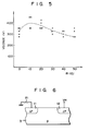
- Fig. 5 shows the voltages applied to the high voltage terminal VH when the MOS transistors TR13 and TR14 were broken when the value of the resistor Rl is set to 0, 10, 20, 30, 40, and 50 ohms (n).
- this high voltage was charged in a capacitor of 200 pF, this capacitor was connected to the high voltage terminal VH by use of a switch, thereby allowing this high voltage to be applied to the high voltage terminal VH.
- this high voltage was changed by 25 V at a time.
- a black dot indicates a voltage applied to the high voltage terminal VH when the MOS transistor TR14 of each sample was broken, while a mark x represents a voltage applied to the high voltage terminal VH when the MOS transistor TR13 of each sample was broken.
- Fig. 6 shows a semiconductor device which can be used in place of the MOS transistor TR14 shown in Fig. 4.
- This semiconductor device is constituted similarly to that shown in Fig. 4 except that the gate electrode 14 is removed.
- the p-type substrate 3 and n +- type regions 11 and 12 form the base, emitter and collector of a bipolar transistor, respectively.
- Fig. 7 shows a semiconductor circuit which is used in place of the MOS transistor TR14 and resistor Rl shown in Fig. 3.
- This semiconductor circuit includes a depletion type (D-type) MOS transistor TR15 which is grounded through a capacitor Cl and in which one end of a current path is connected to the high voltage terminal VH and the other end is connected to a gate thereof; and a gate controlled diode GCD whose gate is connected to the junction between the MOS transistor TR15 and the capacitor C1.
- D-type MOS transistor TR15 depletion type MOS transistor TR15 which is grounded through a capacitor Cl and in which one end of a current path is connected to the high voltage terminal VH and the other end is connected to a gate thereof; and a gate controlled diode GCD whose gate is connected to the junction between the MOS transistor TR15 and the capacitor C1.
- the gate controlled diode GCD is constituted by an n +- type region 15 formed in the surface area of the p-type substrate 3; a gate insulation film 16 formed on a portion of the p-type substrate 3 and on a portion of the n +- type region 15; and a gate electrode 17 formed on the gate insulation film 16.
- This gate electrode 17 is connected to a gate terminal VG which is coupled with the junction between the MOS transistor TR15 and the capacitor Cl.
- the n +- type region 15 is connected to the high voltage terminal VH.
- the substrate 3 is grounded.
- the gate controlled diode GCD having a structure as shown in Fig. 8, the relation between the gate voltage VG and the avalanche breakdown voltage applied to the high voltage terminal VH when a breakdown of the diode GCD occurred is as shown in Fig. 9.
- the gate voltage VG when the gate voltage VG is 0 V, the breakdown voltage is at its lowest point. In the embodiment, this gate voltage - breakdown voltage characteristic is used. Practically speaking, when the high voltage terminal VH is disconnected from the power source, the gate voltage VG is set at 0 V to cause a breakdown of the diode GCD at a low breakdown voltage, thereby preventing the MOS transistor TR13 from being broken, as shown in Fi g . 3.
- the gate voltage VG is set at the VH level and the breakdown voltage of the diode GCD is raised, thereby preventing the MOS transistor TR13 and diode GCD from being broken.
- the gate voltage VG slowly increases due to a time constant which is determined by the MOS transistor TR15 and capacitor Cl, so that a breakdown of the diode GCD occurs at a voltage lower than the breakdown voltage of the MOS transistor TR13.
- the charges produced by the static electricity are discharged rapidly through this diode GCD, in which the breakdown occurred, thereby preventing the MOS transistor TR13 from being broken due to the high voltage which is applied to the high voltage terminal VH and steeply rises.
- Fig. 10 is a modified form of the semiconductor integrated circuit shown in Fig. 7.
- This semiconductor integrated circuit is constituted similarly to that shown in Fig. 7 except that in place of the capacitor Cl, a D-type MOS transistor TR16 whose current path is connected between a power source terminal VC adapted to receive the operating voltage of, e.g., 5 V and the MOS transistor TR16, and whose gate is grounded is used.
- a D-type MOS transistor TR16 whose current path is connected between a power source terminal VC adapted to receive the operating voltage of, e.g., 5 V and the MOS transistor TR16, and whose gate is grounded is used.
- a voltage of, e.g., 5 V is applied to the power source terminal VC and a voltage of 20 V is applied to the high voltage terminal VH.
- the gate voltage of the MOS transistor TR16 is 0 V and a voltage of 5 V is applied to its source, so that the MOS transistor TR16 is kept non-conductive. Therefore, a voltage of 20 V is applied to the gate of the gate controlled diode GCD through the D-type MOS transistor TR15, causing the breakdown voltage of the diode GCD to be greatly increased.
- Fig. 11 shows a semiconductor device which is constituted similarly to that shown in Fig. 8 except that the device of Fig. 11 is provided with an n +- type region 18 formed in the surface area of the p-type substrate 3 at the location apart from the gate insulation layer 16 so as to face the n +- type region 15.
- the gate controlled diode GCD constituted in this way, when an avalanche breakdown of the diode GCD occurs, the potential of the substrate 3 increases and the n +- type regions 15 and 18 and p-type substrate 3 may function as the collector, emitter and base of a bipolar transistor, respectively. Due to this, a large quantity of charges produced at the high voltage terminal VH are discharged to the ground through the n +- type region 15, p-type substrate 3 and n +- type region 18, thereby rapidly lowering the potential at the high voltage terminal VH.
- the present invention has been described above with respect to the embodiments, the invention is not limited to only those embodiments.
- the invention can be also applied to a semiconductor integrated circuit without such a high voltage terminal VH. Namely, even in the MOS transistor having the structure shown in Fig. 2, in which the operation voltage of 5 V instead of the high voltage of 20 V is supplied to the drain, there is a case where when this drain is disconnected from the power source, an abnormally high voltage is applied to this drain due to the static electricity.
- the use of the protecting circuits as shown in Figs. 3, 7 and 10 makes it possible to prevent a similar breakdown of the MOS transistor in the manner as described above.
- the capacitor Cl may be omitted in the case where the parasitic capacitance between the gate of the gate controlled diode GCD and the ground is large.
Landscapes
- Metal-Oxide And Bipolar Metal-Oxide Semiconductor Integrated Circuits (AREA)
- Semiconductor Integrated Circuits (AREA)
Applications Claiming Priority (4)
| Application Number | Priority Date | Filing Date | Title |
|---|---|---|---|
| JP63584/84 | 1984-03-31 | ||
| JP59063583A JPS60207365A (ja) | 1984-03-31 | 1984-03-31 | 半導体集積回路 |
| JP63583/84 | 1984-03-31 | ||
| JP6358484A JPH0626240B2 (ja) | 1984-03-31 | 1984-03-31 | 半導体集積回路 |
Publications (3)
| Publication Number | Publication Date |
|---|---|
| EP0157389A2 true EP0157389A2 (fr) | 1985-10-09 |
| EP0157389A3 EP0157389A3 (en) | 1986-11-20 |
| EP0157389B1 EP0157389B1 (fr) | 1991-06-26 |
Family
ID=26404708
Family Applications (1)
| Application Number | Title | Priority Date | Filing Date |
|---|---|---|---|
| EP85103818A Expired EP0157389B1 (fr) | 1984-03-31 | 1985-03-29 | Dispositif de protection pour un transistor MOS |
Country Status (3)
| Country | Link |
|---|---|
| US (1) | US4725915A (fr) |
| EP (1) | EP0157389B1 (fr) |
| DE (1) | DE3583301D1 (fr) |
Cited By (2)
| Publication number | Priority date | Publication date | Assignee | Title |
|---|---|---|---|---|
| EP0301521A1 (fr) * | 1987-07-29 | 1989-02-01 | Kabushiki Kaisha Toshiba | Dispositif semi-conducteur de mémoire non volatile |
| GB2274203A (en) * | 1993-01-07 | 1994-07-13 | Seiko Epson Corp | Semiconductor device protection |
Families Citing this family (7)
| Publication number | Priority date | Publication date | Assignee | Title |
|---|---|---|---|---|
| KR900008746B1 (ko) * | 1986-11-19 | 1990-11-29 | 삼성전자 주식회사 | 접합 파괴장치 반도체장치 |
| JP3199808B2 (ja) * | 1991-05-14 | 2001-08-20 | セイコーインスツルメンツ株式会社 | 半導体集積回路装置 |
| US5371395A (en) * | 1992-05-06 | 1994-12-06 | Xerox Corporation | High voltage input pad protection circuitry |
| US5428498A (en) * | 1992-09-28 | 1995-06-27 | Xerox Corporation | Office environment level electrostatic discharge protection |
| JP3111943B2 (ja) * | 1997-10-16 | 2000-11-27 | 日本電気株式会社 | 半導体集積回路 |
| US6794719B2 (en) * | 2001-06-28 | 2004-09-21 | Koninklijke Philips Electronics N.V. | HV-SOI LDMOS device with integrated diode to improve reliability and avalanche ruggedness |
| US20060176638A1 (en) * | 2005-02-10 | 2006-08-10 | Fultec Semiconductors, Inc. | Minimized wire bonds in transient blocking unit packaging |
Family Cites Families (9)
| Publication number | Priority date | Publication date | Assignee | Title |
|---|---|---|---|---|
| US3518454A (en) * | 1967-10-20 | 1970-06-30 | Bell Telephone Labor Inc | Bidirectional transmission circuit |
| US3512058A (en) * | 1968-04-10 | 1970-05-12 | Rca Corp | High voltage transient protection for an insulated gate field effect transistor |
| GB1518984A (en) * | 1974-07-16 | 1978-07-26 | Nippon Electric Co | Integrated circuit |
| JPS54136278A (en) * | 1978-04-14 | 1979-10-23 | Nec Corp | Semiconductor device |
| JPS56118371A (en) * | 1980-02-22 | 1981-09-17 | Fujitsu Ltd | Semiconductor integrated circuit device |
| US4342045A (en) * | 1980-04-28 | 1982-07-27 | Advanced Micro Devices, Inc. | Input protection device for integrated circuits |
| IT1150062B (it) * | 1980-11-19 | 1986-12-10 | Ates Componenti Elettron | Protezione di ingresso per circuito integrato di tipo mos, a bassa tensione di alimentazione e ad alta densita' di integrazione |
| US4602267A (en) * | 1981-02-17 | 1986-07-22 | Fujitsu Limited | Protection element for semiconductor device |
| US4527213A (en) * | 1981-11-27 | 1985-07-02 | Tokyo Shibaura Denki Kabushiki Kaisha | Semiconductor integrated circuit device with circuits for protecting an input section against an external surge |
-
1985
- 1985-03-29 US US06/717,695 patent/US4725915A/en not_active Expired - Lifetime
- 1985-03-29 DE DE8585103818T patent/DE3583301D1/de not_active Expired - Lifetime
- 1985-03-29 EP EP85103818A patent/EP0157389B1/fr not_active Expired
Cited By (5)
| Publication number | Priority date | Publication date | Assignee | Title |
|---|---|---|---|---|
| EP0301521A1 (fr) * | 1987-07-29 | 1989-02-01 | Kabushiki Kaisha Toshiba | Dispositif semi-conducteur de mémoire non volatile |
| US5010520A (en) * | 1987-07-29 | 1991-04-23 | Kabushiki Kaisha Toshiba | Nonvolatile semiconductor memory device with stabilized data write characteristic |
| GB2274203A (en) * | 1993-01-07 | 1994-07-13 | Seiko Epson Corp | Semiconductor device protection |
| GB2274203B (en) * | 1993-01-07 | 1996-08-07 | Seiko Epson Corp | Semiconductor device |
| US5614752A (en) * | 1993-01-07 | 1997-03-25 | Seiko Epson Corporation | Semiconductor device containing external surge protection component |
Also Published As
| Publication number | Publication date |
|---|---|
| EP0157389A3 (en) | 1986-11-20 |
| EP0157389B1 (fr) | 1991-06-26 |
| US4725915A (en) | 1988-02-16 |
| DE3583301D1 (de) | 1991-08-01 |
Similar Documents
| Publication | Publication Date | Title |
|---|---|---|
| US5072273A (en) | Low trigger voltage SCR protection device and structure | |
| US5079608A (en) | Power MOSFET transistor circuit with active clamp | |
| US4131908A (en) | Semiconductor protection device having a bipolar lateral transistor | |
| US4449158A (en) | Input protection circuit for MIS transistor | |
| US5010380A (en) | Voltage stress alterable ESD protection structure | |
| US3934159A (en) | Semiconductor circuit devices using insulated gate-type field effect elements having protective diodes | |
| US4786956A (en) | Input protection device for integrated circuits | |
| US4609931A (en) | Input protection MOS semiconductor device with zener breakdown mechanism | |
| US4481521A (en) | Insulated gate field effect transistor provided with a protective device for a gate insulating film | |
| EP0215493B1 (fr) | Circuit à transistors MOS protégé | |
| US4562454A (en) | Electronic fuse for semiconductor devices | |
| US5281841A (en) | ESD protection element for CMOS integrated circuit | |
| US6329691B1 (en) | Device for protection of sensitive gate dielectrics of advanced non-volatile memory devices from damage due to plasma charging | |
| US4725915A (en) | Semiconductor integrated circuit | |
| US4725875A (en) | Memory cell with diodes providing radiation hardness | |
| KR900004726B1 (ko) | 대규모 집적회로용 보호회로 | |
| US3601625A (en) | Mosic with protection against voltage surges | |
| JPH05267690A (ja) | E2promメモリセル | |
| EP0472592B1 (fr) | Structure et dispositif de protection muni d'un redresseur au silicium commande a basse tension de declenchement | |
| US4649414A (en) | PNPN semiconductor switches | |
| KR970004452B1 (ko) | 정전보호회로 | |
| US4437135A (en) | Semiconductor integrated circuit device | |
| EP0606667A1 (fr) | Dispositif semi-conducteur avec un circuit intégré pourvu de moyens de protection contre des surtensions | |
| EP0106417B1 (fr) | Circuit intégré comportant un dispositif de protection d'entrée | |
| KR930006983B1 (ko) | 불휘발성 반도체메모리장치 |
Legal Events
| Date | Code | Title | Description |
|---|---|---|---|
| PUAI | Public reference made under article 153(3) epc to a published international application that has entered the european phase |
Free format text: ORIGINAL CODE: 0009012 |
|
| 17P | Request for examination filed |
Effective date: 19850329 |
|
| AK | Designated contracting states |
Designated state(s): DE FR GB |
|
| PUAL | Search report despatched |
Free format text: ORIGINAL CODE: 0009013 |
|
| AK | Designated contracting states |
Kind code of ref document: A3 Designated state(s): DE FR GB |
|
| 17Q | First examination report despatched |
Effective date: 19881013 |
|
| GRAA | (expected) grant |
Free format text: ORIGINAL CODE: 0009210 |
|
| AK | Designated contracting states |
Kind code of ref document: B1 Designated state(s): DE FR GB |
|
| REF | Corresponds to: |
Ref document number: 3583301 Country of ref document: DE Date of ref document: 19910801 |
|
| ET | Fr: translation filed | ||
| PLBE | No opposition filed within time limit |
Free format text: ORIGINAL CODE: 0009261 |
|
| STAA | Information on the status of an ep patent application or granted ep patent |
Free format text: STATUS: NO OPPOSITION FILED WITHIN TIME LIMIT |
|
| 26N | No opposition filed | ||
| REG | Reference to a national code |
Ref country code: GB Ref legal event code: 746 Effective date: 19981008 |
|
| REG | Reference to a national code |
Ref country code: FR Ref legal event code: D6 |
|
| REG | Reference to a national code |
Ref country code: GB Ref legal event code: IF02 |
|
| PGFP | Annual fee paid to national office [announced via postgrant information from national office to epo] |
Ref country code: FR Payment date: 20040309 Year of fee payment: 20 |
|
| PGFP | Annual fee paid to national office [announced via postgrant information from national office to epo] |
Ref country code: GB Payment date: 20040324 Year of fee payment: 20 |
|
| PGFP | Annual fee paid to national office [announced via postgrant information from national office to epo] |
Ref country code: DE Payment date: 20040408 Year of fee payment: 20 |
|
| PG25 | Lapsed in a contracting state [announced via postgrant information from national office to epo] |
Ref country code: GB Free format text: LAPSE BECAUSE OF EXPIRATION OF PROTECTION Effective date: 20050328 |
|
| REG | Reference to a national code |
Ref country code: GB Ref legal event code: PE20 |