EP0158197A2 - Démodulateur - Google Patents
Démodulateur Download PDFInfo
- Publication number
- EP0158197A2 EP0158197A2 EP85103430A EP85103430A EP0158197A2 EP 0158197 A2 EP0158197 A2 EP 0158197A2 EP 85103430 A EP85103430 A EP 85103430A EP 85103430 A EP85103430 A EP 85103430A EP 0158197 A2 EP0158197 A2 EP 0158197A2
- Authority
- EP
- European Patent Office
- Prior art keywords
- resistor
- input
- operational amplifier
- resistance value
- partial
- Prior art date
- Legal status (The legal status is an assumption and is not a legal conclusion. Google has not performed a legal analysis and makes no representation as to the accuracy of the status listed.)
- Withdrawn
Links
- 230000005669 field effect Effects 0.000 claims abstract description 11
- 239000010409 thin film Substances 0.000 claims description 2
- 230000003321 amplification Effects 0.000 description 2
- 238000001914 filtration Methods 0.000 description 2
- 238000003199 nucleic acid amplification method Methods 0.000 description 2
- 230000001419 dependent effect Effects 0.000 description 1
- 238000010586 diagram Methods 0.000 description 1
- 230000000694 effects Effects 0.000 description 1
- 230000009466 transformation Effects 0.000 description 1
Images
Classifications
-
- H—ELECTRICITY
- H03—ELECTRONIC CIRCUITRY
- H03D—DEMODULATION OR TRANSFERENCE OF MODULATION FROM ONE CARRIER TO ANOTHER
- H03D1/00—Demodulation of amplitude-modulated oscillations
- H03D1/22—Homodyne or synchrodyne circuits
- H03D1/2272—Homodyne or synchrodyne circuits using FET's
Definitions
- the invention relates to a demodulator of the type specified in the preamble of claim 1.
- Such demodulators or rectifiers are used to convert a sinusoidal signal of a specific frequency into a direct voltage that is proportional to the amplitude of the sinusoidal signal.
- the field effect transistor or FET operated as a switch is driven in such a way that the switch is open during the positive half-wave of the sine wave and the switch is closed during the negative half-wave or vice versa.
- the output voltage of the operational amplifier is then usually given a low-pass filter for filtering out the harmonics that arise.
- the input resistance at the inverting input of the operational amplifier and the negative feedback resistance are dimensioned the same to achieve a voltage gain of the operational amplifier of 1 when the switch is open and approximately -1 when the switch is closed.
- the input resistance at the non-inverting input of the operational amplifier corresponds to approximately half of the other input resistance.
- the known demodulator has a relatively high error which is caused by various influences.
- the invention has for its object to significantly improve a demodulator of the type mentioned with regard to the accuracy in converting the amplitude of a sinusoidal input voltage into an amplitude-proportional output voltage.
- an error in the voltage gain of the operational amplifier is eliminated, which is caused by the fact that when the switch is closed, the volume resistance of the field effect transistor is not infinitely small, but a non-negligible value of z. B. has 30 ⁇ .
- the voltage gain of the operational amplifier during the negative half-wave of the sine signal does not reach the same amount as during the positive half-wave, but remains smaller.
- This error is completely compensated for by the inventive design of the negative feedback resistance of the operational amplifier.
- the amount of voltage amplification is the same in each half-wave of the sine signal.
- an error in the output voltage of the operational amplifier is compensated, which is caused by the input quiescent or bias current of the operational amplifier.
- This error manifests itself in an error voltage (offset voltage) at the output of the operational amplifier which is independent of the input voltage and which is additively superimposed on the output voltage of the demodulator and takes on different amounts when the switch is open and closed. While the offset voltage almost disappears when the switch is open, when the switch is closed it assumes a negative value which is dependent on the input resistance at the non-inverting input of the operational amplifier and on the forward resistance of the FET. This means that the output voltage during the negative half wave of the input voltage is not proportional to its amplitude.
- the inventive division of the input resistance at the non-inverting input of the operational amplifier and the inventive design of the partial resistors completely compensate for this error of the inaccurate amplitude proportionality of the output voltage, namely in that in every half-wave of the sinusoidal input voltage at the demodulator, the constant voltage error caused by the bias current at the output of the operational amplifier is the same amount.
- the amplitude proportionality of the output voltage is granted on average.
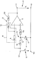
- the drawing shows a circuit diagram of a demodulator for converting a sinusoidal input voltage U E into an output voltage U A proportional to the magnitude of the amplitude.
- the demodulator or rectifier shown in the drawing with its input 10 and its output 11 has an operational amplifier 12, the output of which is fed back via a negative feedback resistor 13 to the inverting input.
- the two inputs of the operational amplifier are each connected via an input resistor 14 or 15 to a connecting terminal 101 of the input 10 of the demodulator which forms the signal input.
- the on the terminal 102 of the input 10 which is at the reference potential of the input signal is connected to the one terminal 112 of the output 11, while the other terminal 111 of the output 11 is connected to the output of the operational amplifier 12.
- the input resistor 15 connected to the non-inverting input of the operational amplifier 12 is divided into two partial resistors 151 and 152.
- the drain of a field effect transistor 17, hereinafter referred to as FET 17 is connected, the source of which is connected to terminal 102 of input 10 and terminal 112 of output 11 of the demodulator, respectively that the FET 17 is connected via the second partial resistor 152 of the input resistor 15 to the non-inverting input of the operational amplifier 12.
- the FET 17 is operated intermittently as a switch in such a way that it opens during the positive half wave of the sinusoidal input voltage U E present at the input 10 of the demodulator (FET 17 blocked) and closes during the negative half wave of the input voltage U E (FET 17 continuously) or vice versa.
- the switch When the switch is open, the voltage gain of the operational amplifier is "+1" and the output voltage U A at the output is always the same as the input voltage U E.
- the switch is closed, that is to say when the FET 17 is turned on, the FET 17 has a forward resistance, the resistance value of which is denoted by R F. Resistance values are understood here and below to be ohmic resistances.
- the Resistance value of the input resistor l4 is with R 1 , the input resistor 15 with R 2 or the partial resistors 151 or 152 with R 21 or R 22 and the negative feedback resistor 13 with R G. designated.
- the negative feedback resistor 13 is also divided into two partial resistors 131 and 132, the resistance values of which are denoted by R G1 and R G2 .
- resistance values are now dimensioned so that they satisfy the following equations: being for G1. (2) it is assumed that the resistance value R G of the negative feedback resistor 13 is approximately equal to the resistance value R 1 of the input resistor 14 (R G ⁇ R 1 ).
- the input resistor 14 at the inverting input of the operational amplifier 12 and the partial resistor Stand 131 of the negative feedback resistor 13 are arranged in thin film technology on a single chip 18, which is symbolized in the drawing by dashed lines. This compensates for a temperature response in these two resistors and has no negative effects on the voltage gain of the operational amplifier 12.
- a transistor can be used instead of the FET, which can be controlled without power.
- another electronic switch for. B. a transistor can be used.
Landscapes
- Engineering & Computer Science (AREA)
- Power Engineering (AREA)
- Amplifiers (AREA)
- Control Of Amplification And Gain Control (AREA)
Applications Claiming Priority (2)
| Application Number | Priority Date | Filing Date | Title |
|---|---|---|---|
| DE3413902 | 1984-04-13 | ||
| DE19843413902 DE3413902A1 (de) | 1984-04-13 | 1984-04-13 | Demodulator |
Publications (2)
| Publication Number | Publication Date |
|---|---|
| EP0158197A2 true EP0158197A2 (fr) | 1985-10-16 |
| EP0158197A3 EP0158197A3 (fr) | 1987-09-02 |
Family
ID=6233445
Family Applications (1)
| Application Number | Title | Priority Date | Filing Date |
|---|---|---|---|
| EP85103430A Withdrawn EP0158197A3 (fr) | 1984-04-13 | 1985-03-22 | Démodulateur |
Country Status (2)
| Country | Link |
|---|---|
| EP (1) | EP0158197A3 (fr) |
| DE (1) | DE3413902A1 (fr) |
Cited By (1)
| Publication number | Priority date | Publication date | Assignee | Title |
|---|---|---|---|---|
| US5949267A (en) * | 1996-10-09 | 1999-09-07 | Nokia Mobile Phones Limited | Circuit arrangement for generating signals with different phases |
Families Citing this family (2)
| Publication number | Priority date | Publication date | Assignee | Title |
|---|---|---|---|---|
| DE29505771U1 (de) * | 1995-04-04 | 1995-05-24 | Christian Schwaiger Kg, 90579 Langenzenn | Wechselspannungsamplituden-Detektionsschaltung |
| DE19616946C2 (de) * | 1996-04-27 | 1998-12-10 | Knick Elektronische Mesgeraete | Vorrichtung zum indirekten Messen von Wechselströmen und -spannungen |
Family Cites Families (1)
| Publication number | Priority date | Publication date | Assignee | Title |
|---|---|---|---|---|
| US4031479A (en) * | 1976-02-23 | 1977-06-21 | The United States Of America As Represented By The Secretary Of The Navy | Peak detecting demodulator |
-
1984
- 1984-04-13 DE DE19843413902 patent/DE3413902A1/de not_active Withdrawn
-
1985
- 1985-03-22 EP EP85103430A patent/EP0158197A3/fr not_active Withdrawn
Cited By (1)
| Publication number | Priority date | Publication date | Assignee | Title |
|---|---|---|---|---|
| US5949267A (en) * | 1996-10-09 | 1999-09-07 | Nokia Mobile Phones Limited | Circuit arrangement for generating signals with different phases |
Also Published As
| Publication number | Publication date |
|---|---|
| EP0158197A3 (fr) | 1987-09-02 |
| DE3413902A1 (de) | 1985-10-24 |
Similar Documents
| Publication | Publication Date | Title |
|---|---|---|
| DE2748647C2 (de) | Verstärker für elektrische Signale | |
| DE3836805A1 (de) | Isolationsverstaerker mit genauem spannungs/arbeitszyklus-konverter, niedriger brummspannung, grosser bandbreite und ladungsabgeglichenem demodulator | |
| DE1938776A1 (de) | Hochleistungs-Messverstaerker | |
| DE2258690C3 (de) | Schaltung zum Vergleichen der Werte zweier Impedanzen | |
| DE2617488A1 (de) | Schaltungsanordnung zur temperaturkompensation bei einem quarzoszillator | |
| DE1438969B2 (de) | Stabilisiertes gleichstromversorgungsgeraet | |
| DE2023842A1 (de) | Trennschaltung | |
| DE1945125B2 (de) | Analogmultiplikator | |
| DE3000291C2 (de) | Schaltungsanordnung zur Umwandlung einer Widerstandsänderung in eine Frequenzänderung | |
| EP0052221A1 (fr) | Circuit de traitement de signaux | |
| DE3413902A1 (de) | Demodulator | |
| DE2329579C3 (de) | Quadrier- oder Effektivwertgleichrichter-Schaltung | |
| DE1183136B (de) | Regelstufe zur automatischen Verstaerkungsregelung | |
| DE1512342B2 (fr) | ||
| DE2810951C2 (de) | Kompensationsschaltung für elektronische Meßgeräte | |
| DE3143669A1 (de) | Schaltung zum messen des effektivwertes einer wechselspannung | |
| AT392709B (de) | Elektronische multiplizierschaltung | |
| DE2422030C3 (de) | Gleichrichter für amplitudenmodulierte elektrische Hochfrequenzschwingungen | |
| DE2950369C2 (de) | Schaltungsanordnung zur Verschiebung des Ausgangsstrombereich es eines Operationsverstärkers | |
| DE2814784C3 (de) | Schalteinrichtung | |
| DE2627293B2 (de) | Verfahren und Vorrichtung zur elektronischen Regelung der Blindleistung eines elektrischen Wechselstromnetzes | |
| DE2329254A1 (de) | Stromwandler mit aktivem lastabschluss | |
| DE1438969C (de) | Stabilisiertes Gleichstromversorgungsgerät | |
| DE2131335C3 (de) | Elektrische Schaltungsanordnung zur Ermittlung der Phasenlage eines Wechselstromsignals | |
| DE2531475B2 (de) | Schaltungsanordnung mit einer steuerbaren impedanz |
Legal Events
| Date | Code | Title | Description |
|---|---|---|---|
| PUAI | Public reference made under article 153(3) epc to a published international application that has entered the european phase |
Free format text: ORIGINAL CODE: 0009012 |
|
| AK | Designated contracting states |
Designated state(s): AT BE CH DE FR GB IT LI LU NL SE |
|
| PUAL | Search report despatched |
Free format text: ORIGINAL CODE: 0009013 |
|
| AK | Designated contracting states |
Kind code of ref document: A3 Designated state(s): AT BE CH DE FR GB IT LI LU NL SE |
|
| 17P | Request for examination filed |
Effective date: 19870922 |
|
| 17Q | First examination report despatched |
Effective date: 19891002 |
|
| STAA | Information on the status of an ep patent application or granted ep patent |
Free format text: STATUS: THE APPLICATION HAS BEEN WITHDRAWN |
|
| 18W | Application withdrawn |
Withdrawal date: 19900525 |
|
| RIN1 | Information on inventor provided before grant (corrected) |
Inventor name: WEILAND, WALTER |