EP0158565B1 - Verfahren zur Herstellung eines Halbleiterlaserspiegels mittels ionischer Bearbeitung - Google Patents
Verfahren zur Herstellung eines Halbleiterlaserspiegels mittels ionischer Bearbeitung Download PDFInfo
- Publication number
- EP0158565B1 EP0158565B1 EP85400624A EP85400624A EP0158565B1 EP 0158565 B1 EP0158565 B1 EP 0158565B1 EP 85400624 A EP85400624 A EP 85400624A EP 85400624 A EP85400624 A EP 85400624A EP 0158565 B1 EP0158565 B1 EP 0158565B1
- Authority
- EP
- European Patent Office
- Prior art keywords
- laser
- mask
- faces
- layer
- machining
- Prior art date
- Legal status (The legal status is an assumption and is not a legal conclusion. Google has not performed a legal analysis and makes no representation as to the accuracy of the status listed.)
- Expired
Links
- 238000000034 method Methods 0.000 title claims description 28
- 239000004065 semiconductor Substances 0.000 title claims description 17
- 230000008569 process Effects 0.000 title claims description 9
- 238000010276 construction Methods 0.000 title 1
- 238000000992 sputter etching Methods 0.000 title 1
- 238000003754 machining Methods 0.000 claims description 29
- 239000000758 substrate Substances 0.000 claims description 21
- 238000005530 etching Methods 0.000 claims description 10
- 238000000407 epitaxy Methods 0.000 claims description 3
- 239000000126 substance Substances 0.000 description 23
- 150000002500 ions Chemical class 0.000 description 18
- 239000000243 solution Substances 0.000 description 15
- XKRFYHLGVUSROY-UHFFFAOYSA-N Argon Chemical compound [Ar] XKRFYHLGVUSROY-UHFFFAOYSA-N 0.000 description 12
- 238000004519 manufacturing process Methods 0.000 description 12
- VEXZGXHMUGYJMC-UHFFFAOYSA-N Hydrochloric acid Chemical compound Cl VEXZGXHMUGYJMC-UHFFFAOYSA-N 0.000 description 11
- 229910001218 Gallium arsenide Inorganic materials 0.000 description 10
- 238000003776 cleavage reaction Methods 0.000 description 9
- 239000000463 material Substances 0.000 description 9
- 239000013078 crystal Substances 0.000 description 8
- 230000007017 scission Effects 0.000 description 8
- 229910052786 argon Inorganic materials 0.000 description 7
- 230000007547 defect Effects 0.000 description 7
- 238000010884 ion-beam technique Methods 0.000 description 7
- 239000000203 mixture Substances 0.000 description 5
- 230000001133 acceleration Effects 0.000 description 4
- 230000000694 effects Effects 0.000 description 4
- 238000010849 ion bombardment Methods 0.000 description 4
- 230000000873 masking effect Effects 0.000 description 4
- 230000003287 optical effect Effects 0.000 description 4
- 238000006243 chemical reaction Methods 0.000 description 3
- 239000011347 resin Substances 0.000 description 3
- 229920005989 resin Polymers 0.000 description 3
- 241001415961 Gaviidae Species 0.000 description 2
- VYPSYNLAJGMNEJ-UHFFFAOYSA-N Silicium dioxide Chemical compound O=[Si]=O VYPSYNLAJGMNEJ-UHFFFAOYSA-N 0.000 description 2
- -1 argon ions Chemical class 0.000 description 2
- YFXPPSKYMBTNAV-UHFFFAOYSA-N bensultap Chemical compound C=1C=CC=CC=1S(=O)(=O)SCC(N(C)C)CSS(=O)(=O)C1=CC=CC=C1 YFXPPSKYMBTNAV-UHFFFAOYSA-N 0.000 description 2
- 230000015572 biosynthetic process Effects 0.000 description 2
- 230000008878 coupling Effects 0.000 description 2
- 238000010168 coupling process Methods 0.000 description 2
- 238000005859 coupling reaction Methods 0.000 description 2
- 230000007423 decrease Effects 0.000 description 2
- 238000000151 deposition Methods 0.000 description 2
- 239000007789 gas Substances 0.000 description 2
- PCHJSUWPFVWCPO-UHFFFAOYSA-N gold Chemical compound [Au] PCHJSUWPFVWCPO-UHFFFAOYSA-N 0.000 description 2
- 239000010931 gold Substances 0.000 description 2
- 229910052737 gold Inorganic materials 0.000 description 2
- 230000006872 improvement Effects 0.000 description 2
- 239000013307 optical fiber Substances 0.000 description 2
- 230000005855 radiation Effects 0.000 description 2
- 230000035939 shock Effects 0.000 description 2
- 239000006104 solid solution Substances 0.000 description 2
- 238000001228 spectrum Methods 0.000 description 2
- 229910018072 Al 2 O 3 Inorganic materials 0.000 description 1
- BYMMIQCVDHHYGG-UHFFFAOYSA-N Cl.OP(O)(O)=O Chemical compound Cl.OP(O)(O)=O BYMMIQCVDHHYGG-UHFFFAOYSA-N 0.000 description 1
- RTAQQCXQSZGOHL-UHFFFAOYSA-N Titanium Chemical compound [Ti] RTAQQCXQSZGOHL-UHFFFAOYSA-N 0.000 description 1
- MODGUXHMLLXODK-UHFFFAOYSA-N [Br].CO Chemical compound [Br].CO MODGUXHMLLXODK-UHFFFAOYSA-N 0.000 description 1
- 229910045601 alloy Inorganic materials 0.000 description 1
- 239000000956 alloy Substances 0.000 description 1
- PNEYBMLMFCGWSK-UHFFFAOYSA-N aluminium oxide Inorganic materials [O-2].[O-2].[O-2].[Al+3].[Al+3] PNEYBMLMFCGWSK-UHFFFAOYSA-N 0.000 description 1
- 230000005540 biological transmission Effects 0.000 description 1
- 238000009933 burial Methods 0.000 description 1
- 239000003153 chemical reaction reagent Substances 0.000 description 1
- 238000011109 contamination Methods 0.000 description 1
- 229910052593 corundum Inorganic materials 0.000 description 1
- 239000002178 crystalline material Substances 0.000 description 1
- 230000008021 deposition Effects 0.000 description 1
- 238000001312 dry etching Methods 0.000 description 1
- 230000005684 electric field Effects 0.000 description 1
- 230000008030 elimination Effects 0.000 description 1
- 238000003379 elimination reaction Methods 0.000 description 1
- 239000000835 fiber Substances 0.000 description 1
- 230000036541 health Effects 0.000 description 1
- 230000010354 integration Effects 0.000 description 1
- 239000007788 liquid Substances 0.000 description 1
- 238000004020 luminiscence type Methods 0.000 description 1
- 230000007246 mechanism Effects 0.000 description 1
- 229910052751 metal Inorganic materials 0.000 description 1
- 239000002184 metal Substances 0.000 description 1
- 238000001465 metallisation Methods 0.000 description 1
- 230000010355 oscillation Effects 0.000 description 1
- 238000005424 photoluminescence Methods 0.000 description 1
- 230000000135 prohibitive effect Effects 0.000 description 1
- 230000009467 reduction Effects 0.000 description 1
- 239000000377 silicon dioxide Substances 0.000 description 1
- 235000012239 silicon dioxide Nutrition 0.000 description 1
- 239000010936 titanium Substances 0.000 description 1
- 229910052719 titanium Inorganic materials 0.000 description 1
- 229910001845 yogo sapphire Inorganic materials 0.000 description 1
Images


Classifications
-
- H—ELECTRICITY
- H01—ELECTRIC ELEMENTS
- H01S—DEVICES USING THE PROCESS OF LIGHT AMPLIFICATION BY STIMULATED EMISSION OF RADIATION [LASER] TO AMPLIFY OR GENERATE LIGHT; DEVICES USING STIMULATED EMISSION OF ELECTROMAGNETIC RADIATION IN WAVE RANGES OTHER THAN OPTICAL
- H01S5/00—Semiconductor lasers
- H01S5/02—Structural details or components not essential to laser action
- H01S5/028—Coatings ; Treatment of the laser facets, e.g. etching, passivation layers or reflecting layers
Definitions
- the subject of the present invention is a method of producing a semiconductor laser mirror, by ion machining.
- a double heterostructure consists of a stack of thin layers of different semiconductor alloys, these layers being deposited on a monocrystalline substrate, either by epitaxy in liquid or gas phase, or by molecular beam.
- the active region where both light radiation and electron-hole pairs are confined has the shape of a ribbon whose width is about ten microns and the length included between 100 and 300 ilm. This length is that which separates the two cleaved faces of the crystal, faces which form the mirrors of the resonant cavity of the laser.
- the privileged field of semiconductor lasers is that of optical telecommunications.
- the materials constituting the layers of the double heterostructure are taken from the family of ternary solid solutions of general formula Ga 1-x Al x As where x is between 0 and 1
- the layers are epitaxied on a GaAs substrate.
- the materials constituting the layers are taken from the family of quaternary solid solutions of general formula Ga 1-x ln x As 1-y P y where y is between 0 and 1.
- the layers are epitaxially grown on an InP substrate.
- RIE dry reactive chemical attack
- the object of the invention is to overcome the difficulties encountered in these different techniques.
- the invention recommends the use of ionic machining for the production of one or more mirrors of the laser, and this under particular masking conditions.
- Ion machining is an etching technique widely used in the production of current electronic devices (integrated circuits). This is a dry etching using ions (argon for example) accelerated by an electric field in an ion gun, in particular of the KAUFMAN type. These accelerated ions fall on a target from where they drive out the atoms by a mechanism of transfer of momentum.
- ions argon for example
- Ion machining has an essential characteristic which is the directivity of the ion beam used. This directivity makes it possible to precisely control the slope of the engraved wall.
- the interest of ionic machining to make laser mirrors was described by the applicant during the Conference entitled "Second European Conference on Integrated Optics" which was held in Florence (Italy) on October 17 and 18, 1983 ( Conference Publication No. 227, pages 24-26).
- the present invention relates to the conditions for implementing this technique and aims to improve the quality of the mirrors obtained.
- the improvement provided by the present invention mainly relates to the masking step occurring during the ion bombardment operation.
- the use of the usual mask materials has proved unsatisfactory for deep ionic machining (of the order of 4-5 ⁇ m). In all cases, the faces obtained are rough and their flatness poor. The applicant has found that the origin of these defects was due to the poor definition of the mask used.
- the applicant proposes to use, as a mask, a layer of crystalline material opaque to the ion beam, this layer being delimited laterally by at least one face constituting the side of the mask, this face being a crystallographic plane. of the material used. In this way, the side of the mask is perfectly defined and the ionic machining operation, which is carried out through this mask, leads to perfect etching, the etched side is smooth and flat.
- the invention therefore relates to a method of producing a semiconductor laser mirror by ion machining, in which a semiconductor structure is subjected to ion bombardment through a mask whose side determines the location of the mirror to be machined, this process being characterized by the fact that this mask is constituted by a crystalline layer whose side is a crystallographic plane.
- the mask is obtained by epitaxy of a crystalline layer on the semiconductor structure, then by chemical attack on this layer to form the crystallographic plane.
- the mask consists of a thin strip with cleaved faces placed and preferably bonded to the semiconductor structure.
- the ion bombardment takes place in a direction inclined relative to the plane perpendicular to the semiconductor structure. It has been observed, in fact, by the applicant, that with normal incidence, an etching plane is obtained which is slightly inclined with respect to the plane normal to the structure (angle of the order of 27 °). By increasing the angle of incidence of the beam compared to normal, the obliquity of the machined face decreases.
- the inclination of the incident ion beam relative to the sample to be machined can be carried out in two different ways either by directly tilting the rotating substrate holder on which the sample is placed, or by placing the sample on a block making an angle a with the substrate holder which remains horizontal. A perfectly vertical face can be obtained for an angle of incidence close to 230 using the first technique and 12 ° using the second technique.
- the basic structure constituting the laser will not be described in detail since it is widely known. It suffices to recall that it is a double heterostructure generally comprising a first confinement layer, an active layer, a second confinement layer, a contact layer and a metallic layer.
- the semiconductor layers undergo a proton bombardment intended to delimit an active ribbon.
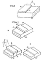
- Figure 1 shows such a heterostructure 10 on which has been deposited an epitaxial layer 12 serving as a mask for an etching operation symbolized by the arrows 14.
- the epitaxial layer 12 has a sidewall 16 which is a crystallographic plane for the crystal constituting the layer 12. This plane is obtained by chemical attack on the layer 12. This chemical attack is carried out in a conventional manner by protecting the epitaxial layer 12 by a mask whose edge defines the flank 16.
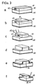
- Figure 2a illustrates another variant in which the mask is a thin strip 20, cleaved along two faces 21, 22 and bonded to a heterostructure 24.
- the strip can be made of GaAs for example and the crystallographic planes of cleavage can correspond, for example, to the crystal orientations (110 ) or (110).
- FIG. 2b illustrates the step of ionic machining with an ion beam 30 whose direction makes an angle ⁇ with the normal to the structure. This angle can be around twenty degrees.
- a step 32 is then obtained, the flank 34 of which is vertical and perfectly smooth and flat.
- FIG. 2c illustrates the mesa 32 obtained after elimination of the mask 20.
- the face 34 constitutes the reflecting face forming a mirror.
- the method of the invention makes it possible to avoid these difficulties as will be seen in the following two examples.
- Such a laser can be produced using a double heterostructure GaAIAs on GaAs or GaInAsP on InP.
- the bar 46 forming the mask consists of a thin layer of Ga x Al 1-x As with x greater than about 0.5 epitaxially grown on the substrate .
- Tests carried out by the applicant have made it possible to obtain lasers with a split face and a machined face for which the threshold currents measured were typically 120 mA for ribbons of 12 ⁇ m wide and cavity lengths of 380 ⁇ m and 18 mA for buried tapes 5.5 ⁇ m wide and cavity lengths of 60 ⁇ m. These threshold current values are equivalent to those obtained with lasers of the same length and with two cleaved faces.
- Such a laser can only be produced using a double GaInAsP heterostructure on InP because InP has different chemical attack properties than those of other III-V materials. Indeed, there are chemical solutions such as pure hydrochloric acid (HCI) or hydrochloric acid-orthophosphoric acid mixture (HCI-H 3 P0 4 ), for which certain crystallographic planes of InP have very low attack speeds compared to other plans. This difference in attack speeds has the effect of showing the planes for which the speeds are the lowest. These plans thus form the profiles of the mesas obtained.
- HCI hydrochloric acid
- HCI-H 3 P0 4 hydrochloric acid-orthophosphoric acid mixture
- the planes (110) and (110) are perpendicular to the planes (001) of the substrate and have an almost zero attack speed. After chemical attack in a pure HCl solution, rectangular mesas with straight edges can then be formed. However, no other solution has shown similar effects on GaAs or on GalnAsP.
- the laser obtained has two reflective faces 86, 88 obtained by ion machining.
- This structure poses the delicate problem of its connection to an optical fiber. Indeed, as the edge of the laser (which is at the level of the active layer 66) does not coincide with the edge of the substrate 62, it is difficult to put an optical fiber of a few tens of microns in diameter in immediate contact with the laser . For this reason, we may prefer a structure with only one side pickled by ionic machining, the other side being cleaved.
- the production steps are identical to those of the laser described above, except that instead of using a U-shaped mask, an H-shaped mask is used. This mask is shown in top view in FIG. 5. It bears the reference 100.
- the active ribbon bears the reference 102.
- the structure is cleaved in the middle, along a cleavage plane 104.
- the method of the invention also makes it possible to produce more complex structures than those which have just been described.
- These are structures comprising not only a laser but also an optical guide or a photodetector (for example a photodiode). This is included in a feedback loop used to adjust the laser supply current according to the detected power.
- Such a device is shown in FIG. 6. It comprises a laser formed by a double heterostructure 110 deposited on a substrate 111, this heterostructure comprising in particular an active layer 112. Opposite this laser, another heterostructure 114 operates as a photodetector; it has an active layer 116 located in the plane of the layer 120 and which receives part 118 of the radiation emitted by the laser.
- the assembly also includes ohmic contacts 115, 117 and 119.
- the groove separating the laser 110 and the photodetector 114 is obtained in the case of a double heterostructure in InP, by the method of the invention, that is to say by ionic machining through a mask with a crystallographic flank.
- the mask is pierced with an opening corresponding to the groove to be engraved.
- an ion beam 120 inclined relative to the normal is used (to obtain, as explained above, a reflecting face 122 perpendicular to the plane of the layers of the heterostructure) one obtains, on the side of the photodiode, an etched face 123 which is substantially inclined relative to the normal plane.
- this arrangement makes it possible to eliminate any risk of feedback due to a reflection of the beam 118 on the face 123 with reinjection into the laser 110.
- the production of the groove by ion machining makes it possible to obtain a very small width of the order of 10 ⁇ m, which strengthens the coupling between the laser 110 and the photodiode 114.
- Figure 7 shows, in section, the previous elements during the ion machining operation.
- the mask 125 has flanks 126 and 127 which are, according to the essential characteristic of the invention, crystallographic planes.
- the index-guided ribbon lasers have improved laser performance compared to gain-guided structures (reduction of threshold current, improvement in power-current linearity, mode stability and above all possibility of operating in only one longitudinal mode).
- gain-guided structures reduction of threshold current, improvement in power-current linearity, mode stability and above all possibility of operating in only one longitudinal mode.
- a longitudinal single-mode laser is not suitable as a light source for transmissions by multimode fibers. Longitudinal multimode operation is preferable. Such an operation can be obtained in index-guided structures, provided that the ribbon is inclined by relation to the direction perpendicular to the plane of the cleaved faces.
- This arrangement can be easily obtained by machining the two faces of the laser in two directions parallel to each other but at an angle of a few degrees relative to the direction of the ribbon. This is what is illustrated in FIG. 8 where we see a structure 130 of the buried ribbon type, limited by faces 131, 132, inclined by a dangle 0 relative to the plane perpendicular to the direction of the ribbon.
- one of the two diodes operates as a laser, the other as a frequency modulator, which makes it possible to stabilize the oscillation mode.
- Such a device has made it possible to obtain stable longitudinal single-mode spectra, even at high modulation frequencies.
- FIG. 9 shows a device of this type, obtained by a very simple production method which uses the technique of the invention described above.
- a heterostructure 140 having an active ribbon 142, and bounded by two cleaved faces 144 and 145.
- a mask is placed having an opening of approximately 5 ⁇ m, this opening being perpendicular to the direction of the active ribbon.
- the sides of this mask are crystallographic planes.
- an ionic machining is carried out which has the effect of digging a groove 146 delimited by two faces 148, 149.
- an emitting laser 150 is obtained and on the other a modulator device 152
- the two devices are integrated on the same support.
- the machining process which has just been described with the aid of these various examples is essentially based on removal of material by ion bombardment.
- the incident ions transfer significant amounts of movement to the atoms of the crystal lattice and thus cause their uprooting. But these shocks also induce crystal defects.
- the degree of disturbance of the bombarded surface depends on the acceleration voltage of the ions the lower this voltage the less the defects created are important. But the engraving speed decreases with tension. A compromise must therefore be found in order to obtain a satisfactory etching speed while limiting the disturbance of the machined surface.
- a first etching can be carried out with a voltage of 500 volts and an ion current density of 0.5 mA / cm 2 for one hour, immediately followed by a second etching at a voltage of 300 Volts and an ion density of 0.2 mA / cm 2 for a few tens of minutes.
- the first etching with high acceleration voltage and high argon pressure makes it possible to reach a depth of approximately 5 ⁇ m, which generally corresponds to the total thickness of the layers of a conventional double heterostructure.
- the second etching, at low acceleration voltage and at low argon pressure, makes it possible to strip the surface obtained after the first attack by creating a slightly disturbed surface.
- Residual defects can be definitively eliminated by immersing the sample for a few seconds in a chemical solution composed of 1 volume of H 2 SO 4 , 8 8 volumes of H 2 0 2 and 1 volume of H 2 0 at 0 ° C, in the case of GaAs or in a mixture of bromemethanol at 5% o in the case of InP.
Landscapes
- Physics & Mathematics (AREA)
- Condensed Matter Physics & Semiconductors (AREA)
- General Physics & Mathematics (AREA)
- Electromagnetism (AREA)
- Optics & Photonics (AREA)
- Semiconductor Lasers (AREA)
- Drying Of Semiconductors (AREA)
Claims (4)
Applications Claiming Priority (2)
| Application Number | Priority Date | Filing Date | Title |
|---|---|---|---|
| FR8405223A FR2562339B1 (fr) | 1984-04-03 | 1984-04-03 | Procede de realisation d'un miroir de laser a semi-conducteur, par usinage ionique |
| FR8405223 | 1984-04-03 |
Publications (2)
| Publication Number | Publication Date |
|---|---|
| EP0158565A1 EP0158565A1 (de) | 1985-10-16 |
| EP0158565B1 true EP0158565B1 (de) | 1988-06-08 |
Family
ID=9302778
Family Applications (1)
| Application Number | Title | Priority Date | Filing Date |
|---|---|---|---|
| EP85400624A Expired EP0158565B1 (de) | 1984-04-03 | 1985-03-29 | Verfahren zur Herstellung eines Halbleiterlaserspiegels mittels ionischer Bearbeitung |
Country Status (6)
| Country | Link |
|---|---|
| US (1) | US4865684A (de) |
| EP (1) | EP0158565B1 (de) |
| JP (1) | JPS61501739A (de) |
| DE (1) | DE3563285D1 (de) |
| FR (1) | FR2562339B1 (de) |
| WO (1) | WO1985004529A1 (de) |
Families Citing this family (8)
| Publication number | Priority date | Publication date | Assignee | Title |
|---|---|---|---|---|
| DE3738053A1 (de) * | 1987-11-09 | 1989-05-18 | Siemens Ag | Laseranordnung mit mindestens einem laserresonator und einem damit verkoppelten passiven resonator |
| KR900009229B1 (ko) * | 1988-04-28 | 1990-12-24 | 한국 과학기술원 | 선택적 에피택시법에 의한 표면 방출형 AlGaAs/GaAs 반도체 레이저 다이오드의 제조방법 |
| JP2991716B2 (ja) * | 1988-08-16 | 1999-12-20 | 三菱化学株式会社 | エッチトミラー型化合物半導体レーザー装置及び集積素子 |
| US5259925A (en) * | 1992-06-05 | 1993-11-09 | Mcdonnell Douglas Corporation | Method of cleaning a plurality of semiconductor devices |
| JPH0677181A (ja) * | 1992-08-26 | 1994-03-18 | Matsushita Electric Ind Co Ltd | 化合物半導体の微細構造形成方法 |
| KR0178492B1 (ko) * | 1995-12-21 | 1999-04-15 | 양승택 | 기울어진 공진기로 편광특성이 제어된 표면방출 레이저 다이오드 제조방법 |
| JPH09298339A (ja) * | 1996-04-30 | 1997-11-18 | Rohm Co Ltd | 半導体レーザの製法 |
| US6781099B2 (en) * | 2001-03-12 | 2004-08-24 | Karl-Heinz Krah Gmbh | Electrofusion socket forming system |
Family Cites Families (7)
| Publication number | Priority date | Publication date | Assignee | Title |
|---|---|---|---|---|
| US4248688A (en) * | 1979-09-04 | 1981-02-03 | International Business Machines Corporation | Ion milling of thin metal films |
| US4354898A (en) * | 1981-06-24 | 1982-10-19 | Bell Telephone Laboratories, Incorporated | Method of preferentially etching optically flat mirror facets in InGaAsP/InP heterostructures |
| NL8104068A (nl) * | 1981-09-02 | 1983-04-05 | Philips Nv | Halfgeleiderlaser. |
| DE3138704A1 (de) * | 1981-09-29 | 1983-04-21 | Siemens AG, 1000 Berlin und 8000 München | Verfahren zur herstellung von laserdioden-resonatorspiegeln |
| FR2525033B1 (fr) * | 1982-04-08 | 1986-01-17 | Bouadma Noureddine | Laser a semi-conducteur a plusieurs longueurs d'onde independantes et son procede de realisation |
| US4397711A (en) * | 1982-10-01 | 1983-08-09 | Bell Telephone Laboratories, Incorporated | Crystallographic etching of III-V semiconductor materials |
| JPS59219974A (ja) * | 1983-05-27 | 1984-12-11 | Matsushita Electric Ind Co Ltd | 半導体レ−ザの製造方法 |
-
1984
- 1984-04-03 FR FR8405223A patent/FR2562339B1/fr not_active Expired
-
1985
- 1985-03-29 EP EP85400624A patent/EP0158565B1/de not_active Expired
- 1985-03-29 DE DE8585400624T patent/DE3563285D1/de not_active Expired
- 1985-04-01 JP JP60501611A patent/JPS61501739A/ja active Pending
- 1985-04-01 WO PCT/FR1985/000072 patent/WO1985004529A1/fr not_active Ceased
-
1988
- 1988-02-12 US US07/158,071 patent/US4865684A/en not_active Expired - Fee Related
Also Published As
| Publication number | Publication date |
|---|---|
| US4865684A (en) | 1989-09-12 |
| DE3563285D1 (en) | 1988-07-14 |
| WO1985004529A1 (fr) | 1985-10-10 |
| JPS61501739A (ja) | 1986-08-14 |
| FR2562339B1 (fr) | 1986-06-20 |
| EP0158565A1 (de) | 1985-10-16 |
| FR2562339A1 (fr) | 1985-10-04 |
Similar Documents
| Publication | Publication Date | Title |
|---|---|---|
| EP0829934B1 (de) | Herstellungsverfahren einer optoelektrischen Halbleitervorrichtung, und Vorrichtung oder Matrix von Vorrichtungen hergestellt unter Verwendung dieses Verfahrens | |
| US7009216B2 (en) | Semiconductor light emitting device and method of fabricating the same | |
| US6277696B1 (en) | Surface emitting laser using two wafer bonded mirrors | |
| EP0222639A1 (de) | Herstellungsverfahren einer integrierten Laserphotodetektor-Struktur | |
| EP0091859B1 (de) | Verfahren zur Herstellung eines Halbleiterlasers mit mehreren unabhängigen Wellenlängen | |
| FR3053538A1 (fr) | Source laser a semi-conducteur | |
| EP0887668A1 (de) | Bragg-Reflektor in einem Halbleiter und Herstellungsverfahren | |
| EP0158565B1 (de) | Verfahren zur Herstellung eines Halbleiterlaserspiegels mittels ionischer Bearbeitung | |
| EP0817337B1 (de) | Herstellungsverfahren für einen Oberflächenemittierenden Laser | |
| EP0776075B1 (de) | Laservorrichtung, insbesondere zum optischen Pumpen | |
| JPH1056234A (ja) | 改善された半導体レーザおよびそれを製造する方法 | |
| EP0501862B1 (de) | Verfahren zur Herstellung eines Halbleiterlasers mit vergrabener Streifenstruktur unter Verwendung von Trockenätzen zur Herstellung dieses Streifens und ein nach diesem Verfahren hergestellter Laser | |
| EP0580495A1 (de) | Verfahren zur Herstellung einer Struktur für Lichtwellenleiter und integrierte Spiegel und so hergestellte Struktur | |
| EP0664588A1 (de) | Halbleiterstruktur mit virtuellem Beugungsgitter | |
| CA2251280A1 (fr) | Amplificateur optique semi-conducteur et source laser integree l'incorporant | |
| EP0580717B1 (de) | Optoelektronische vorrichtung mit einer sehr niedrigen parasitischen kapazitat und verfahren zu ihrer herstellung | |
| FR2502847A1 (fr) | Dispositif emetteur de lumiere a semi-conducteurs comportant une structure de canalisation du courant | |
| EP0402249B1 (de) | Wellenlängenstabilisierter Halbleiterlaser | |
| EP0096613B1 (de) | Halbleiter-Laservorrichtung mit einem Wellenleiter, der durch einen Gradienten im Brechungsindex gebildet ist und Verfahren zur Herstellung einer solchen Vorrichtung | |
| EP0187581A1 (de) | Lichtsende- und -empfangsdioden und integrierte optische Einwegtransmissionselemente und Verfahren zu ihrer Herstellung | |
| EP1233494A1 (de) | Halbleiterlaser miet vergrabener Streifenstruktur und Herstellungsverfahren | |
| FR3074372A1 (fr) | Structure a gain, dispositif photonique comprenant une telle structure et procede de fabrication d'une telle structure a gain | |
| EP1339144A1 (de) | Optische halbleitervorrichtung | |
| FR2744225A1 (fr) | Procede pour la realisation d'un plan incline a 45 degres sur un composant cristallin 3-5 et composant optique | |
| FR2897726A1 (fr) | Source optique laser a emission verticale |
Legal Events
| Date | Code | Title | Description |
|---|---|---|---|
| PUAI | Public reference made under article 153(3) epc to a published international application that has entered the european phase |
Free format text: ORIGINAL CODE: 0009012 |
|
| AK | Designated contracting states |
Designated state(s): DE GB NL |
|
| 17P | Request for examination filed |
Effective date: 19860321 |
|
| 17Q | First examination report despatched |
Effective date: 19870804 |
|
| GRAA | (expected) grant |
Free format text: ORIGINAL CODE: 0009210 |
|
| AK | Designated contracting states |
Kind code of ref document: B1 Designated state(s): DE GB NL |
|
| REF | Corresponds to: |
Ref document number: 3563285 Country of ref document: DE Date of ref document: 19880714 |
|
| GBT | Gb: translation of ep patent filed (gb section 77(6)(a)/1977) | ||
| PLBE | No opposition filed within time limit |
Free format text: ORIGINAL CODE: 0009261 |
|
| STAA | Information on the status of an ep patent application or granted ep patent |
Free format text: STATUS: NO OPPOSITION FILED WITHIN TIME LIMIT |
|
| 26N | No opposition filed | ||
| PGFP | Annual fee paid to national office [announced via postgrant information from national office to epo] |
Ref country code: DE Payment date: 19940314 Year of fee payment: 10 |
|
| PGFP | Annual fee paid to national office [announced via postgrant information from national office to epo] |
Ref country code: GB Payment date: 19940322 Year of fee payment: 10 |
|
| PGFP | Annual fee paid to national office [announced via postgrant information from national office to epo] |
Ref country code: NL Payment date: 19940331 Year of fee payment: 10 |
|
| PG25 | Lapsed in a contracting state [announced via postgrant information from national office to epo] |
Ref country code: GB Effective date: 19950329 |
|
| PG25 | Lapsed in a contracting state [announced via postgrant information from national office to epo] |
Ref country code: NL Effective date: 19951001 |
|
| GBPC | Gb: european patent ceased through non-payment of renewal fee |
Effective date: 19950329 |
|
| NLV4 | Nl: lapsed or anulled due to non-payment of the annual fee |
Effective date: 19951001 |
|
| PG25 | Lapsed in a contracting state [announced via postgrant information from national office to epo] |
Ref country code: DE Effective date: 19951201 |