EP0158756A2 - Dispositif pour l'insertion des fils de contact de composants électriques dans des trous correspondants suivant les espacements différents de ces trous - Google Patents
Dispositif pour l'insertion des fils de contact de composants électriques dans des trous correspondants suivant les espacements différents de ces trous Download PDFInfo
- Publication number
- EP0158756A2 EP0158756A2 EP84402104A EP84402104A EP0158756A2 EP 0158756 A2 EP0158756 A2 EP 0158756A2 EP 84402104 A EP84402104 A EP 84402104A EP 84402104 A EP84402104 A EP 84402104A EP 0158756 A2 EP0158756 A2 EP 0158756A2
- Authority
- EP
- European Patent Office
- Prior art keywords
- mid
- plane
- lead
- spacing
- holes
- Prior art date
- Legal status (The legal status is an assumption and is not a legal conclusion. Google has not performed a legal analysis and makes no representation as to the accuracy of the status listed.)
- Granted
Links
Images

Classifications
-
- H—ELECTRICITY
- H05—ELECTRIC TECHNIQUES NOT OTHERWISE PROVIDED FOR
- H05K—PRINTED CIRCUITS; CASINGS OR CONSTRUCTIONAL DETAILS OF ELECTRIC APPARATUS; MANUFACTURE OF ASSEMBLAGES OF ELECTRICAL COMPONENTS
- H05K13/00—Apparatus or processes specially adapted for manufacturing or adjusting assemblages of electric components
- H05K13/04—Mounting of components, e.g. of leadless components
- H05K13/043—Feeding one by one by other means than belts
- H05K13/0439—Feeding one by one by other means than belts incorporating means for treating the terminal leads only before insertion
-
- Y—GENERAL TAGGING OF NEW TECHNOLOGICAL DEVELOPMENTS; GENERAL TAGGING OF CROSS-SECTIONAL TECHNOLOGIES SPANNING OVER SEVERAL SECTIONS OF THE IPC; TECHNICAL SUBJECTS COVERED BY FORMER USPC CROSS-REFERENCE ART COLLECTIONS [XRACs] AND DIGESTS
- Y10—TECHNICAL SUBJECTS COVERED BY FORMER USPC
- Y10T—TECHNICAL SUBJECTS COVERED BY FORMER US CLASSIFICATION
- Y10T29/00—Metal working
- Y10T29/49—Method of mechanical manufacture
- Y10T29/49002—Electrical device making
- Y10T29/49117—Conductor or circuit manufacturing
- Y10T29/49124—On flat or curved insulated base, e.g., printed circuit, etc.
- Y10T29/49147—Assembling terminal to base
- Y10T29/49151—Assembling terminal to base by deforming or shaping
- Y10T29/49153—Assembling terminal to base by deforming or shaping with shaping or forcing terminal into base aperture
-
- Y—GENERAL TAGGING OF NEW TECHNOLOGICAL DEVELOPMENTS; GENERAL TAGGING OF CROSS-SECTIONAL TECHNOLOGIES SPANNING OVER SEVERAL SECTIONS OF THE IPC; TECHNICAL SUBJECTS COVERED BY FORMER USPC CROSS-REFERENCE ART COLLECTIONS [XRACs] AND DIGESTS
- Y10—TECHNICAL SUBJECTS COVERED BY FORMER USPC
- Y10T—TECHNICAL SUBJECTS COVERED BY FORMER US CLASSIFICATION
- Y10T29/00—Metal working
- Y10T29/53—Means to assemble or disassemble
- Y10T29/5313—Means to assemble electrical device
- Y10T29/53174—Means to fasten electrical component to wiring board, base, or substrate
- Y10T29/53183—Multilead component
Definitions
- the present invention is directed toward an improved method and apparatus for insertion of the leads of electronic components into the corresponding holes of a circuit board,. wherein an insertion tooling is automatically adjustable to accommodate axial lead components having body portions of varying lengths and wherein this tooling is "lead driving", i.e., drivingly engages the leads rather than the bodies of the components.
- the improvement is directed to adaptation of these insertion heads to such component mountings via corresponding circuit board holes which are much more closely spaced than prior art variable spacing "lead driving" insert tooling has been able to handle.
- the invention is directed to insertion of axial lead electronic components into spaced holes of a circuit board wherein the center-to-center spacings of the holes are 5 mm. and greater.
- Prior art variable center distance machines like - those cross-referenced above have not been adaptable to insertion of components into 5 mm. center-to-center hole spacings by lead driving without changing the driver blades for such insertions.
- the prior art insertion apparatus for 5 mm. center-to-center hole spacings has employed tooling which drivingly engages the body of the component or fixed insertion heads, wherein the component lead severing, bending and driving tools incorporated within the insertion head are not relatively adjustable, i.e., such devices have been dedicated to 5 mm. insertion.
- an additional insertion head was required for "lead driving" insertion into 5 mm. hole spacings along with larger hole spacings in the same circuit board.
- a primary object of the present invention is to provide a "lead driving" insertion methoo and apparatus which overcomes the above-mentioned necessity for an insertion head dedicated to 5 mm. hole spacings.
- an insertion head having a pair of tooling sections which are adjustable, by spreading or closing relative to a mid-plane, so as to permit a component to be inserted into a board on any desired lead center or center distance (C.D.).
- C.D. lead center or center distance
- the ability of the same insertion head to insert on variable lead centers permits versatility of circuit board design and terminal arrangement, while providing maximum circuit board population density. Still greater density and versatility may be realized by use of the invention to make insertions in 5 mm. hole spacings.
- driver blades similar to those disclosed in the above cross-referenced Patent No. Re. 27,968, which will allow closing of the spaced tooling sections sufficiently to handle components having body lengths of 0.150 inches for "lead driving" insertion into 5 mm.
- the thickness of the driver blades it is necessary to reduce the thickness of the driver blades.
- misinsertion of particular leads can and do occur during a subsequent clinching operation by kicking an inserted lead out from under the reduced thickness of the driver blade.
- the instant invention overcomes such difficulties by spacing the driver blades of reduced thickness from the outside formers of such insertion heads when handling insertions in greater hole spacings. In this manner, a reduced thickness blade does not ride upon the radius of a formed lead sufficiently to lose control of such a lead during the subsequent clinching operation.
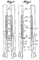
- prior art machines to which the instant invention is particularly applicable include insertion tooling sections 103 which are variably movable in directions perpendicular to a mid-plane 8 in order to adjust to various lengths of component bodies 3 prior to trimming and forming leads 5 for subsequent insertion into the holes of circuit board 6.
- Each tooling section 103 includes an outside former 149, an inside former 131, and driver blades 145, with relative vertical movement between inside formers 131 and outside formers 149 forming the leads 5 for subsequent insertion into the holes of circuit board 6 by driving engagement of drivers 145, as is clearly discernible from these drawings and the above cross-referenced patents.
- the instant invention is directed to a method and apparatus by which variable tooling sections of the lead driving type are able to handle components and insert the leads thereof into circuit board holes which have center-to-center spacings typically 0.197-0.800 inches in range. It is important to keep in mind that, typically, the component has a maximum body length of 0.150 inches, and a maximum lead diameter of 0.020 inches for insertion into minimum hole diameters on the order of 0.040 inches. Further, since the leads 5 must be formed or bent sufficiently close to body 3 for subsequent insertion into the 5 mm. hole spacings, there is a physical limit to the thickness that each driver 145 may be in order to pass between an end of body 3 and the corresponding outside former l49 without crushing body 3 during such insertion.
- driver blade 145 is not as critical.
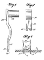
- a problem arises upon spreading of tool sections 103 that the reduced thickness driver blade l45 is engaging each lead 5 at substantially the formed radius thereof without being limited inwardly by body 3, so that during a subsequent clinching operation (by an apparatus illustrated in phantom lines in Fig. lC) a lead may be forced or kicked out from under driving engagement with a driver.
- a lead misinsertion is illustrated by phantom lined lead 7 in Fig. 8.
- driver blades 145 sufficiently thin as to handle components for insertion into 5 mm. hole spacings, while particularly adapting such thin driver blades to provide insertion of components into the larger hole spacings up to about 0.800 inches, without loss of control of the leads by the driver blades as by "kick-out" during a subsequent clinching operation.
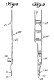
- Such provision has been accomplished by providing a blade 145 of blue spring steel which is configured for removable mounting within a slot 12 of each driver body 20 and is held therein by engagement of latch portion 29 of blade 145 within orifice .18 of the driver body 145.
- Each blade 145 is particularly configured to have a spring portion 27 near the middle thereof so as to aid in retention of,blade 145 within driver body 20 and to bias tip 22 of each blade 145 toward mid-plane 8.
- Stop knobs 28 are provided on each blade 145 in order to limit the inward closing of blade tips 22 upon mid-plane 8. In the 5 mm. hole spacing described above, each stop knob 28 is typically 0.085 inches in length and each blade 145 is configured such that the tips thereof can close to no less a spacing than 0.150 inches.
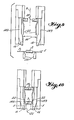
- Outside formers 149 are configured such that blade tips 22 may be flexed outwardly past the inside surfaces of outside formers 149. After forming of a lead and during actuation of the driver 145 to engage and drive the formed lead, camming surface 14 of each outside former 149 will ensure proper engagement of a tip 22 with the formed lead while allowing maximum spreading of tips 22 and sliding engagement with the inside surfaces of outside formers 149 during insertion.
- driver blades 145 are so close to the body 3 of the component as illustrated in Fig. 10, no inside "kick-out" of the leads by the subsequent clinching operation may occur when handling components to be inserted in such small hole spacings.
- the lead misinsertion of Fig. 8 can occur with reduced thickness driver blades.
- Such a "kick-out" problem for larger hole spacings has been overcome by the particular configuration and mounting of the blades 145 such that, upon spreading of tooling sections 103 so that stop knobs 28 do not engage, driver blade tips 22 will be sprung inwardly away from engagement with the inside surfaces of outside formers 149.
- driver blade tips 22 This inward springing or spacing of driver blade tips 22 from the inside surfaces of outside formers 149 causes engagement of the tips 22 with portions of the formed leads which are substantially not on the formed radius thereof. Accordingly, the driver blade tips 22 appear thicker to the formed leads, and the above described "kick-out" of a lead in the clinching operation is avoided.
Landscapes
- Engineering & Computer Science (AREA)
- Manufacturing & Machinery (AREA)
- Microelectronics & Electronic Packaging (AREA)
- Supply And Installment Of Electrical Components (AREA)
- Lead Frames For Integrated Circuits (AREA)
Priority Applications (1)
| Application Number | Priority Date | Filing Date | Title |
|---|---|---|---|
| AT84402104T ATE43469T1 (de) | 1984-03-27 | 1984-10-19 | Vorrichtung zum einsetzen von anschlussdraehten elektrischer komponenten in uebereinstimmende loecher, gemaess verschiedenen abstaenden zwischen diesen loechern. |
Applications Claiming Priority (2)
| Application Number | Priority Date | Filing Date | Title |
|---|---|---|---|
| US06/593,929 US4625399A (en) | 1984-03-27 | 1984-03-27 | Method and apparatus for inserting leads of electrical components into corresponding holes according to different spacings of said holes |
| US593929 | 1984-03-27 |
Publications (3)
| Publication Number | Publication Date |
|---|---|
| EP0158756A2 true EP0158756A2 (fr) | 1985-10-23 |
| EP0158756A3 EP0158756A3 (en) | 1986-09-10 |
| EP0158756B1 EP0158756B1 (fr) | 1989-05-24 |
Family
ID=24376794
Family Applications (1)
| Application Number | Title | Priority Date | Filing Date |
|---|---|---|---|
| EP84402104A Expired EP0158756B1 (fr) | 1984-03-27 | 1984-10-19 | Dispositif pour l'insertion des fils de contact de composants électriques dans des trous correspondants suivant les espacements différents de ces trous |
Country Status (6)
| Country | Link |
|---|---|
| US (1) | US4625399A (fr) |
| EP (1) | EP0158756B1 (fr) |
| JP (1) | JPS60214600A (fr) |
| AT (1) | ATE43469T1 (fr) |
| CA (1) | CA1222833A (fr) |
| DE (1) | DE3478385D1 (fr) |
Families Citing this family (6)
| Publication number | Priority date | Publication date | Assignee | Title |
|---|---|---|---|---|
| US4727647A (en) * | 1986-08-18 | 1988-03-01 | Universal Instruments Corporation | VCD tooling for DIP components of different widths |
| US4833776A (en) * | 1988-01-29 | 1989-05-30 | Westinghouse Electric Corp. | Tactile retrieval and insertion and method for electronic components in through-hole printed circuit boards |
| GB9719520D0 (en) * | 1997-09-12 | 1997-11-19 | Kci Medical Ltd | Surgical drape and suction heads for wound treatment |
| US20070115652A1 (en) * | 2003-12-31 | 2007-05-24 | Simoni Jacquelyn R | Hands-free flashlight suspended from neck of user |
| EP3086628B1 (fr) * | 2015-04-21 | 2018-07-18 | Braun GmbH | Composant électrique spécial, ensemble de carte de circuit imprimé et procédé de fabrication d'un appareil électrique |
| CN113519208B (zh) * | 2019-03-08 | 2023-08-18 | 株式会社富士 | 折弯装置、元件供给装置及折弯方法 |
Family Cites Families (8)
| Publication number | Priority date | Publication date | Assignee | Title |
|---|---|---|---|---|
| US3167780A (en) * | 1962-12-05 | 1965-02-02 | Burroughs Corp | Machine for cutting, forming and inserting leads of electrical components |
| US3594887A (en) * | 1969-03-19 | 1971-07-27 | Amp Inc | Apparatus for electrically connecting pairs of conductors |
| US3593404A (en) * | 1969-11-14 | 1971-07-20 | Universal Instruments Corp | Multisize dual center distance electronic component insertion machine |
| USRE27968E (en) * | 1973-07-19 | 1974-04-09 | Multisize variable center electronic component insertion machine | |
| JPS55118691A (en) * | 1979-03-07 | 1980-09-11 | Matsushita Electric Industrial Co Ltd | Device for inserting multiikind size electric part |
| JPS5628397A (en) * | 1979-08-10 | 1981-03-19 | Kawasaki Heavy Ind Ltd | Freezing protective structure for low-temperature underground tank bottom |
| US4417683A (en) * | 1981-11-09 | 1983-11-29 | Universal Instruments Corporation | Centering device for electrical components |
| US4470182A (en) * | 1982-07-01 | 1984-09-11 | Universal Instruments Corporation | Method and apparatus for centering electrical components |
-
1984
- 1984-03-27 US US06/593,929 patent/US4625399A/en not_active Expired - Fee Related
- 1984-10-19 AT AT84402104T patent/ATE43469T1/de not_active IP Right Cessation
- 1984-10-19 DE DE8484402104T patent/DE3478385D1/de not_active Expired
- 1984-10-19 EP EP84402104A patent/EP0158756B1/fr not_active Expired
- 1984-10-23 CA CA000466152A patent/CA1222833A/fr not_active Expired
-
1985
- 1985-03-22 JP JP60055758A patent/JPS60214600A/ja active Pending
Also Published As
| Publication number | Publication date |
|---|---|
| ATE43469T1 (de) | 1989-06-15 |
| JPS60214600A (ja) | 1985-10-26 |
| EP0158756A3 (en) | 1986-09-10 |
| EP0158756B1 (fr) | 1989-05-24 |
| US4625399A (en) | 1986-12-02 |
| CA1222833A (fr) | 1987-06-09 |
| DE3478385D1 (en) | 1989-06-29 |
Similar Documents
| Publication | Publication Date | Title |
|---|---|---|
| DE69006440T2 (de) | Abgeschirmter Steckverbinder. | |
| US3951494A (en) | Electrical connector | |
| DE60209094T2 (de) | Vorrichtung und Verfahren zum Anschliessen von Kabeln | |
| DE69815017T2 (de) | Entfernung von Leiterplatten | |
| US4625399A (en) | Method and apparatus for inserting leads of electrical components into corresponding holes according to different spacings of said holes | |
| US4108028A (en) | Wire stripper having replaceable blades | |
| USRE30342E (en) | Wire stripper having replaceable blades | |
| US5099570A (en) | Self aligning inserter | |
| US3833993A (en) | Crimping apparatus | |
| US4399844A (en) | Component lead bending and crimping tool | |
| US4369819A (en) | Lead wire forming apparatus for electric parts | |
| EP3431232B1 (fr) | Coupe-bornes pour retirer les bornes d'une bande de support | |
| WO1991003083A1 (fr) | Support pour une combinaison de fiche/douille | |
| CA1093286A (fr) | Traduction non-disponible | |
| US4470182A (en) | Method and apparatus for centering electrical components | |
| EP3772611A1 (fr) | Système de réalisation d'un luminaire doté d'un préhenseur électrique avec porte-conducteur | |
| US4704790A (en) | Method and apparatus for attaching components to substrates | |
| US4512071A (en) | Tool holder | |
| DE2949432C2 (de) | Stecksicherung | |
| US3797107A (en) | Backplane manufacture | |
| EP0270480A2 (fr) | Appareil pour le raccordement d'âmes de câble au contacts tranchants et serrants de blocs de connexion "drop wire" de télécommunications | |
| US4945953A (en) | Surface mount component jig | |
| US4188704A (en) | Hand tool and loader | |
| DE69606336T2 (de) | Steckverbinderhaltevorrichtung | |
| EP0849843A2 (fr) | Dispositif pour aligner un câble-ruban à un connecteur |
Legal Events
| Date | Code | Title | Description |
|---|---|---|---|
| PUAI | Public reference made under article 153(3) epc to a published international application that has entered the european phase |
Free format text: ORIGINAL CODE: 0009012 |
|
| AK | Designated contracting states |
Designated state(s): AT BE CH DE FR GB IT LI LU NL SE |
|
| PUAL | Search report despatched |
Free format text: ORIGINAL CODE: 0009013 |
|
| AK | Designated contracting states |
Kind code of ref document: A3 Designated state(s): AT BE CH DE FR GB IT LI LU NL SE |
|
| 17P | Request for examination filed |
Effective date: 19861114 |
|
| 17Q | First examination report despatched |
Effective date: 19880418 |
|
| GRAA | (expected) grant |
Free format text: ORIGINAL CODE: 0009210 |
|
| AK | Designated contracting states |
Kind code of ref document: B1 Designated state(s): AT BE CH DE FR GB IT LI LU NL SE |
|
| PG25 | Lapsed in a contracting state [announced via postgrant information from national office to epo] |
Ref country code: SE Effective date: 19890524 Ref country code: LI Effective date: 19890524 Ref country code: IT Free format text: LAPSE BECAUSE OF FAILURE TO SUBMIT A TRANSLATION OF THE DESCRIPTION OR TO PAY THE FEE WITHIN THE PRESCRIBED TIME-LIMIT;WARNING: LAPSES OF ITALIAN PATENTS WITH EFFECTIVE DATE BEFORE 2007 MAY HAVE OCCURRED AT ANY TIME BEFORE 2007. THE CORRECT EFFECTIVE DATE MAY BE DIFFERENT FROM THE ONE RECORDED. Effective date: 19890524 Ref country code: CH Effective date: 19890524 Ref country code: BE Effective date: 19890524 Ref country code: AT Effective date: 19890524 |
|
| REF | Corresponds to: |
Ref document number: 43469 Country of ref document: AT Date of ref document: 19890615 Kind code of ref document: T |
|
| REF | Corresponds to: |
Ref document number: 3478385 Country of ref document: DE Date of ref document: 19890629 |
|
| ET | Fr: translation filed | ||
| REG | Reference to a national code |
Ref country code: CH Ref legal event code: PL |
|
| PGFP | Annual fee paid to national office [announced via postgrant information from national office to epo] |
Ref country code: GB Payment date: 19890930 Year of fee payment: 6 |
|
| PGFP | Annual fee paid to national office [announced via postgrant information from national office to epo] |
Ref country code: DE Payment date: 19891011 Year of fee payment: 6 |
|
| PGFP | Annual fee paid to national office [announced via postgrant information from national office to epo] |
Ref country code: FR Payment date: 19891030 Year of fee payment: 6 |
|
| PG25 | Lapsed in a contracting state [announced via postgrant information from national office to epo] |
Ref country code: LU Free format text: LAPSE BECAUSE OF NON-PAYMENT OF DUE FEES Effective date: 19891031 |
|
| PGFP | Annual fee paid to national office [announced via postgrant information from national office to epo] |
Ref country code: NL Payment date: 19891031 Year of fee payment: 6 |
|
| PLBE | No opposition filed within time limit |
Free format text: ORIGINAL CODE: 0009261 |
|
| STAA | Information on the status of an ep patent application or granted ep patent |
Free format text: STATUS: NO OPPOSITION FILED WITHIN TIME LIMIT |
|
| 26N | No opposition filed | ||
| PG25 | Lapsed in a contracting state [announced via postgrant information from national office to epo] |
Ref country code: GB Effective date: 19901019 |
|
| PG25 | Lapsed in a contracting state [announced via postgrant information from national office to epo] |
Ref country code: NL Effective date: 19910501 |
|
| NLV4 | Nl: lapsed or anulled due to non-payment of the annual fee | ||
| GBPC | Gb: european patent ceased through non-payment of renewal fee | ||
| PG25 | Lapsed in a contracting state [announced via postgrant information from national office to epo] |
Ref country code: FR Effective date: 19910628 |
|
| PG25 | Lapsed in a contracting state [announced via postgrant information from national office to epo] |
Ref country code: DE Effective date: 19910702 |
|
| REG | Reference to a national code |
Ref country code: FR Ref legal event code: ST |