EP0158774A2 - Système de traitement de données comprenant un dispositif de vérification de mémoire - Google Patents
Système de traitement de données comprenant un dispositif de vérification de mémoire Download PDFInfo
- Publication number
- EP0158774A2 EP0158774A2 EP85101041A EP85101041A EP0158774A2 EP 0158774 A2 EP0158774 A2 EP 0158774A2 EP 85101041 A EP85101041 A EP 85101041A EP 85101041 A EP85101041 A EP 85101041A EP 0158774 A2 EP0158774 A2 EP 0158774A2
- Authority
- EP
- European Patent Office
- Prior art keywords
- data
- serial
- bus
- controller
- parallel
- Prior art date
- Legal status (The legal status is an assumption and is not a legal conclusion. Google has not performed a legal analysis and makes no representation as to the accuracy of the status listed.)
- Granted
Links
Images


Classifications
-
- G—PHYSICS
- G06—COMPUTING OR CALCULATING; COUNTING
- G06F—ELECTRIC DIGITAL DATA PROCESSING
- G06F11/00—Error detection; Error correction; Monitoring
- G06F11/22—Detection or location of defective computer hardware by testing during standby operation or during idle time, e.g. start-up testing
- G06F11/2205—Detection or location of defective computer hardware by testing during standby operation or during idle time, e.g. start-up testing using arrangements specific to the hardware being tested
- G06F11/2221—Detection or location of defective computer hardware by testing during standby operation or during idle time, e.g. start-up testing using arrangements specific to the hardware being tested to test input/output devices or peripheral units
Definitions
- the present invention relates to data processing systems and particularly to a data processing system with an improved storage testing device.
- a whole processor may be contained on a single chip.
- a microprocessor is usually connected with an associated main storage unit through a storage controller which may be an independent integrated circuit chip or may be contained on the same chip as the processor.
- storage channel or bus between processor and main storage through the storage controller is a parallel data bus.
- microprocessor technology In the microprocessor technology, the main storage unit cannot be readily accessed for testing, debugging, and consequent data modification. Accordingly, present microprocessor systems have to a limited extent relied on software routines in the microprocessor system for testing purposes. Such software routines cannot be used for debugging because they require an operational system. They also have limitations in that they cannot check for certain types of hardware errors.
- Another testing and debugging approach has been to attach specialized apparatus to the parallel data bus of the system. However, as the technology moves toward 32-bit parallel buses, the specialized hardware would have to have a very wide interface and run at the system's speed. Such hardware would not be very economical.
- the system of the present invention provides an approach which does not require costly specialized hardware, does not require a wide accessing bus nor extensive software routines stored in the system. It relies on a serial bus to access main storage as well as other I/O devices which completely bypasses the main parallel data bus of the system.
- the present invention is directed to a data processing system comprising a central processor and particularly a microprocessor which outputs data in a parallel format, a main storage unit, a storage control interfacing between the., processor and storage unit, and a parallel data bus between the processor and the controller.
- An expedient for testing and debugging the controller and the storage unit is provided which is simple, easy to implement and utilizes a minimum of additional hardware and/or software.
- a serial data bus is connected to the storage controller completely independent of the parallel data bus connected to said controller.
- the system also includes means for providing serial test data to the serial bus and consequently to the controller.
- the controller contains means for converting the serial data received from the serial bus into the parallel format of the data which would normally be received over the parallel data bus under normal operational conditions in the absence of any testing or debugging procedures.
- testing or debugging data provided over the serial bus is converted into the same format as the parallel data, the testing or debugging procedures can be carried out with very little additional hardware through the storage controller.
- means are provided for disabling the input to the storage controller from the parallel data bus when data is being input into the controller from the serial bus.
- the serial data bus is also connected to such input/output device controllers whereby data over the serial data bus may be simultaneously applied over said data bus to the storage controller as well as to the controllers for said input/output devices.
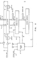
- Processor 12 which serves the function of a central processor in the system is most suitably a microprocessor. It communicates over the system bus 11 which is a parallel data bus preferably 32 bits wide.
- the processor 12 is connected over bus 11 with main system storage 14 via storage controller 13 and storage bus 20.
- the processor is also connected through bus 11 to a plurality of I/O devices,-16 and 18, through their respective I/O device controllers 15 and 17 and I/O buses 21 and 22.
- the I/O devices may be any conventional devices normally associated with a data processing or text processing system, e.g., CRT displays, disk drives, or printers.
- serial data line 19 which represents a bypass to the main parallel data bus 11.
- serial data line 19 may be applied to the storage controller 13 and to main storage 14 for the purpose of testing or debugging storage and storage control.
- the present expedient provides access to I/O devices 16 and 18 via device controllers 15 and 17 which bypasses the main process parallel data bus 11 so as to provide an alternate and simple expedient for modifying I/O device control.
- serial data which is provided to storage controller 13 via lines 19 and 23 may be provided through any supplementary processor such as supporting processor 10.
- Supporting processor 10 may conveniently be an IBM Personal Computer.
- serial clock line 26 which is connected to the controllers through lines 27, 28, and 29. The data on this line is used for timing purposes.
- serial clock signals on line 26 transfer data into and out of storage and the other I/O devices, storage 14 and the other I/O devices 16 and 18, through their respective storage controllers.
- the serial clock signal also controls the initiation of various operations within the controllers.
- serial data line 19 it communicates data from the supporting processor 10 to respective controllers such as a storage controller 13 and transfers data back to the supporting processor from the controller.
- addresses and data commands sent to, for example, storage 14 through storage controller 13 are positive (logical "1" is at the up level), and data read from storage is negative (logical "1" is at the down level).
- Shift buffer 34 is a shift register having 32-bit positions for data plus 4 bit positions for parity checking.
- This shift register is capable of receiving a parallel data input, e.g., over parallel data buses 11 and 38, and providing a parallel data output over parallel data bus 39.
- it is capable of receiving a serial data input over line 41, shifting this serial input in the conventional manner from left to right and providing a serial output over line 42.
- the input from serial data line 19 to shift buffer 34 and the output from shift buffer 34 onto serial data line 19 will be subsequently described in terms of read and write operations through storage controller 13 with respect to storage unit 14.
- shift buffer 34 must contain sufficient storage elements to contain the Request String, Write Data String, and Read Data String operations which will subsequently be described with respect to the flow chart of Fig. 3 and the timing diagram of Fig. 4.
- Start bit latch 35 and stop bit latch 33 are storage elements which contain the start bit and stop bit, respectively, of a data string during such a processing operation.
- the input on serial data line 19 to stop bit latch 33 is applied through gate 31 while the output of shift buffer 34 to serial data line 19 is applied through start bit latch 35 and inverter gate 30.
- Gate 30 provides for the inversion of the output in order that the data read from storage is negative as described herein and above. It should be noted that in order to have this negative signal, the logic in which gate 30 is implemented would be open-collector bipolar logic or open-drain FET logic.
- Shift buffer 34 and its associated circuitry are connected and controlled such that when the serial clock pulse on line 26 is brought to a low level from a high level by an appropriate serial clock signal from processor 10, then serial data signal is placed in stop bit latch 33 (Fig. 2) while the existing contents of stop bit latch 33 are placed in the leftmost bit position of shift buffer 34 and while the rightmost bit of shift buffer 34 is placed in the start bit latch 35.
- Shift buffer 34 also serves a buffer function during normal operations of the data processing system when no testing or debugging is taking place and parallel data bus 11 is not being bypassed. _During such normal operations, the data from parallel data bus 11 is loaded in parallel into shift buffer 34.
- address register 36 Associated with shift buffer 34 and connected with this buffer in parallel through parallel data bus 39 is address register 36.
- Address register 36 consists of storage elements which correspond with and are set in parallel to equivalent elements of shift buffer 34. During a read or write operation to be subsequently described, address register contains the operand address.
- Address comparator 37 serves the function of comparing a request .address received over serial data line 19 with a set of valid addresses for the storage unit 14.
- serial data being input through line 19 has substantially the same command and address circuit as the data output from processor 12 being applied and parallel over bus 11.
- the operand address would have the same structure and format as a conventional operand address.
- control logic block 32 read and write operations will be described with respect to the operational flow chart of Fig. 3.
- the various read and write operations are carried out under the control of supporting processor 10 (Fig. 1) over serial data line 19 when the input from processor 12 along parallel data bus 11 is being bypassed.
- the operations will be described with respect to storage unit 14 via storage controller 13.
- the operation is first reset. Shift buffer 34 is cleared, step 51. Stop bit latch 33 and start bit latch 35 are cleared (i.e., reset to 0's), step 52. In this state all operations are complete. With stop bit latch 15 reset to 0, the serial data signal line 19 is controlled by supporting processor 10 since inverter gate is in the high impedance state (no signal).
- This reset operation may be initiated either by microprocessor 12 or supporting processor 10.
- the logic controlling the operations to be now described is stored in control logic block 32 (Fig. 2).
- control logic block 32 Fig. 2.
- sufficient serial data must be transmitted along line 19 to put to a "1" both start bit latch 35 and stop bit latch 13. This will occur when supporting processor 10 has shifted a correct request string to the controller whereby the request string start bit is now in start bit latch 35 and the request string stop bit is in stop bit latch 33 and the remainder of the request string is contained in shift buffer 34.
- This overall determination is made in decision step 53 of Fig. 3.
- the "1" in start bit latch 35 inverted through inverter gate 30 forces the serial data signal on line 19 low. This low signal is sensed by supporting processor 10 to ensure that the request string was properly sent.
- step 54 senses whether the serial clock signal on line 27 is still low.
- the control logic will not affect the contents of stop bit latch 33 or the shift buffer 34 so long as this serial clock signal remains low.
- step 55 control logic 32 sends a signal along line 43 to shift buffer 34 to load the contents of shift buffer 34 into address register 36.
- step 56 clears stop bit latch 33 and start bit latch 35, step 57.
- step 58 a determination is made as to whether the operation in the address system is a read or write operation. This is carried out by control logic 32 which is connected to address register 36 via line 44 whereby it may inspect the contents of address register 36.
- step 59 the procedure under control logic 32 waits until the start bit latch 35 and the stop bit latch 33 both contain "1". This will occur after the supporting processor 10 has shifted a correct write data stream into shift buffer 34 of storage controller 13. After this has occurred, a determination has still to be made as to whether serial clock signal is low, step 60. As previously described with respect to the request string, the serial data signal is held low by start bit latch 35. At this point, the serial clock signal on line 27 is placed on a high level by supporting processor 10.
- control logic 32 inspects the output of address comparator 37 connected through line 45 in order to determine if the address is in range, i.e., valid, step 61. If the address comparator 37 indicates that the operand address is not valid for the storage unit, then control logic 32 clears shift buffer 34, step 62, as well as stop bit latch 33 in start bit latch 35, step 63, and takes no further action by returning to initial decision step 53.
- control logic 32 initiates the write operation to storage unit 14 through storage controller 13, step 62.
- This write operation should be carried out in substantially the same manner that the routine write operation involving data transferred from processor 12 over parallel data bus would be carried out, i.e., the address for the operation contained in address register 36 is substantially identical in format and structure to a normal address while the data to be stored and contained in shift 34 is substantially identical in format and structure to data transferred to shift buffer 34 from processor 12 via parallel data bus 11 in normal operations.
- step 63 the procedure continues through steps 62 and 63 wherein the shift buffer 34 and the start and stop bits 35 and 33 are cleared. Clearing start bit latch 35 causes a low to high transition on the signal in the serial data bus on the serial data line 19. This signifies to the supporting processor 10 that the write operation is now complete. The procedure is now returned to initial step 53 to wait for another operation.
- step 64 control logic 32 again inspects the output of address comparator 37 on line 45. After the address is compared, then there is an indication that the operand address is valid for storage unit 14.
- step 65 control logic initiates the read operation which again is substantially equivalent to a routine read operation for data which would be applied to shift buffer 34 over parallel data bus 11 from processor 12 based upon the particular address contained in address register 36 with the data being read and transferred to buffer 34 from which may be read out through output 42 and inverter 30 back to supporting processor 10.
- step 66 when the read operation is completed, step 66, then, step 67, data read is contained in shift buffer 34.
- the start bit latch 35 is set to "I", step 68, to cause a high to low transition of the signal on serial data line 19.
- the supporting processor 10 may read the data stream by shifting the contents of shift buffer 34 into start bit latch 35 by applying high to low transition on the serial clock signal on line 27. It should be noted that supporting processor 10 must force the signal on serial data line 19 to "0" on each of these transitions of the signal on serial clock line 27 so that stop bit latch 13 and, consequently, shift buffer 34 will be set to "0's".
- the controller 13 supporting storage unit 14 is ready to accept the next operation and the procedure is again returned to initial step 53.
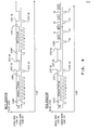
- Fig. 4 is a timing diagram of the data flow along serial data line 19 and the corresponding signals on serial clock line 27 during the three operations of Request String, Write Data String, and Read Data String.
- the timing chart shows the variation of pulse levels with time in the standard manner together with an indication of particular steps in the operation of Fig. 3 which have been completed at the indicated points in the timing chart of Fig. 4.
- each of the Request String, Write Data String, and Read Data String begins with a start bit while th Request String and the Write Data String both end with a stop bit.
- the Request String, Write Data String, and Read Data String contain information identical in format and structure to information which would be transferred from the main data bus 11 to shift buffer 34 during normal operations of the processor system.
- the timing chart illustrates the previously described steps wherein the supporting processor 10 may read the data stream by shifting the contents of shift buffer 34 (Fig. 2) into start bit latch 35 by applying a high to low transition of the clock signal on line 27 (this is shown by pulse 80 on the timing chart).
- the supporting processor 10 must then force the signal on data line 19 to "0" (points 81, 82 and 83 of timing chart) on each respective transition of the clock' signal on line 27 (points 84, 85 and 86 of timing chart) so that stop bit latch 13 and shift buffer 34 will be set to "0's".
Landscapes
- Engineering & Computer Science (AREA)
- General Engineering & Computer Science (AREA)
- Theoretical Computer Science (AREA)
- Computer Hardware Design (AREA)
- Quality & Reliability (AREA)
- Physics & Mathematics (AREA)
- General Physics & Mathematics (AREA)
- Debugging And Monitoring (AREA)
- Techniques For Improving Reliability Of Storages (AREA)
- Test And Diagnosis Of Digital Computers (AREA)
Applications Claiming Priority (2)
| Application Number | Priority Date | Filing Date | Title |
|---|---|---|---|
| US59515984A | 1984-03-30 | 1984-03-30 | |
| US595159 | 1984-03-30 |
Publications (3)
| Publication Number | Publication Date |
|---|---|
| EP0158774A2 true EP0158774A2 (fr) | 1985-10-23 |
| EP0158774A3 EP0158774A3 (en) | 1988-09-14 |
| EP0158774B1 EP0158774B1 (fr) | 1991-01-16 |
Family
ID=24381993
Family Applications (1)
| Application Number | Title | Priority Date | Filing Date |
|---|---|---|---|
| EP19850101041 Expired EP0158774B1 (fr) | 1984-03-30 | 1985-02-01 | Système de traitement de données comprenant un dispositif de vérification de mémoire |
Country Status (3)
| Country | Link |
|---|---|
| EP (1) | EP0158774B1 (fr) |
| JP (1) | JPS60207942A (fr) |
| DE (1) | DE3581308D1 (fr) |
Cited By (4)
| Publication number | Priority date | Publication date | Assignee | Title |
|---|---|---|---|---|
| EP0230219A3 (en) * | 1986-01-14 | 1989-04-05 | International Business Machines Corporation | Apparatus for testing a data processing system |
| EP0457115A3 (en) * | 1990-05-16 | 1992-11-04 | Kabushiki Kaisha Toshiba | Data processing device with test control circuit |
| GB2312533A (en) * | 1996-04-26 | 1997-10-29 | Ibm | Serial bus monitoring and auxiliary control system |
| EP1077412A3 (fr) * | 1999-08-16 | 2004-12-15 | Hewlett-Packard Company, A Delaware Corporation | Système de bus avec procédé de commande amélioré |
Family Cites Families (5)
| Publication number | Priority date | Publication date | Assignee | Title |
|---|---|---|---|---|
| FR2256706A5 (fr) * | 1973-12-27 | 1975-07-25 | Cii | |
| US4023142A (en) * | 1975-04-14 | 1977-05-10 | International Business Machines Corporation | Common diagnostic bus for computer systems to enable testing concurrently with normal system operation |
| JPS5283033A (en) * | 1975-12-29 | 1977-07-11 | Fujitsu Ltd | Memory diagnostic system |
| JPS5833576B2 (ja) * | 1977-03-14 | 1983-07-20 | 株式会社東芝 | 計算機システムの故障診断装置 |
| JPS578858A (en) * | 1980-06-20 | 1982-01-18 | Nec Corp | Integrated circuit package |
-
1984
- 1984-12-17 JP JP59264693A patent/JPS60207942A/ja active Pending
-
1985
- 1985-02-01 DE DE8585101041T patent/DE3581308D1/de not_active Expired - Lifetime
- 1985-02-01 EP EP19850101041 patent/EP0158774B1/fr not_active Expired
Cited By (5)
| Publication number | Priority date | Publication date | Assignee | Title |
|---|---|---|---|---|
| EP0230219A3 (en) * | 1986-01-14 | 1989-04-05 | International Business Machines Corporation | Apparatus for testing a data processing system |
| EP0457115A3 (en) * | 1990-05-16 | 1992-11-04 | Kabushiki Kaisha Toshiba | Data processing device with test control circuit |
| US5363380A (en) * | 1990-05-16 | 1994-11-08 | Kabushiki Kaisha Toshiba | Data processing device with test control circuit |
| GB2312533A (en) * | 1996-04-26 | 1997-10-29 | Ibm | Serial bus monitoring and auxiliary control system |
| EP1077412A3 (fr) * | 1999-08-16 | 2004-12-15 | Hewlett-Packard Company, A Delaware Corporation | Système de bus avec procédé de commande amélioré |
Also Published As
| Publication number | Publication date |
|---|---|
| DE3581308D1 (de) | 1991-02-21 |
| EP0158774A3 (en) | 1988-09-14 |
| EP0158774B1 (fr) | 1991-01-16 |
| JPS60207942A (ja) | 1985-10-19 |
Similar Documents
| Publication | Publication Date | Title |
|---|---|---|
| US4878168A (en) | Bidirectional serial test bus device adapted for control processing unit using parallel information transfer bus | |
| EP0189638B1 (fr) | Adaptateur de largeur de bus | |
| EP0378426B1 (fr) | Transmission de données utilisant les lignes d'adresse d'un bus | |
| US6049894A (en) | Error generation circuit for testing a digital bus | |
| EP0378427B1 (fr) | Transmission de données à haute vitesse sur un bus de système ordinateur | |
| US4023142A (en) | Common diagnostic bus for computer systems to enable testing concurrently with normal system operation | |
| US4253147A (en) | Memory unit with pipelined cycle of operations | |
| US20050114567A1 (en) | Serial peripheral interface (SPI) apparatus with write buffer for improving data throughput | |
| US5155735A (en) | Parity checking apparatus with bus for connecting parity devices and non-parity devices | |
| EP0006472B1 (fr) | Dispositif de microcommande pour commander le transfer bidirectionnel entre une unité de contrôle centrale et une pluralité d'unités externes | |
| EP0485507B1 (fr) | Systeme d'entree/sortie modulaire pour super-ordinateurs | |
| US5784382A (en) | Method and apparatus for dynamically testing a memory within a computer system | |
| US4287563A (en) | Versatile microprocessor bus interface | |
| JPH01133167A (ja) | データ転送ドライバ | |
| US5229999A (en) | Method and apparatus for integrity testing of fault monitoring logic | |
| JPS62182954A (ja) | 一致回路を備えたメモリ装置を含むデ−タ処理装置と方法 | |
| EP0158774B1 (fr) | Système de traitement de données comprenant un dispositif de vérification de mémoire | |
| US4633489A (en) | Interface unit inserted between a data transfer unit and a processor unit | |
| US6202117B1 (en) | Host adapter integrated circuit having autoaccess pause | |
| JPH11502643A (ja) | シリアルデータバスシステムにおけるエラーの認識及び除去 | |
| US6324596B1 (en) | Providing device status during bus retry operations | |
| US6240473B1 (en) | Providing device status during bus retry operations | |
| EP0439594B1 (fr) | Appareil pour connecter un bus de processeur principal connecte a un processeur principal a un bus peripherique connecte a plusieurs appareils perpheriques | |
| KR930011348B1 (ko) | 데코더 ic와 scsi ic간의 인터페이스 회로 | |
| KR0161483B1 (ko) | 메모리를 이용한 마이크로 콘트롤러의 내부 램 데이터 표시장치 |
Legal Events
| Date | Code | Title | Description |
|---|---|---|---|
| PUAI | Public reference made under article 153(3) epc to a published international application that has entered the european phase |
Free format text: ORIGINAL CODE: 0009012 |
|
| AK | Designated contracting states |
Designated state(s): DE FR GB |
|
| 17P | Request for examination filed |
Effective date: 19860124 |
|
| PUAL | Search report despatched |
Free format text: ORIGINAL CODE: 0009013 |
|
| AK | Designated contracting states |
Kind code of ref document: A3 Designated state(s): DE FR GB |
|
| 17Q | First examination report despatched |
Effective date: 19890704 |
|
| GRAA | (expected) grant |
Free format text: ORIGINAL CODE: 0009210 |
|
| AK | Designated contracting states |
Kind code of ref document: B1 Designated state(s): DE FR GB |
|
| REF | Corresponds to: |
Ref document number: 3581308 Country of ref document: DE Date of ref document: 19910221 |
|
| ET | Fr: translation filed | ||
| PLBE | No opposition filed within time limit |
Free format text: ORIGINAL CODE: 0009261 |
|
| STAA | Information on the status of an ep patent application or granted ep patent |
Free format text: STATUS: NO OPPOSITION FILED WITHIN TIME LIMIT |
|
| 26N | No opposition filed | ||
| PGFP | Annual fee paid to national office [announced via postgrant information from national office to epo] |
Ref country code: GB Payment date: 19920113 Year of fee payment: 8 |
|
| PGFP | Annual fee paid to national office [announced via postgrant information from national office to epo] |
Ref country code: FR Payment date: 19920124 Year of fee payment: 8 |
|
| PGFP | Annual fee paid to national office [announced via postgrant information from national office to epo] |
Ref country code: DE Payment date: 19920304 Year of fee payment: 8 |
|
| PG25 | Lapsed in a contracting state [announced via postgrant information from national office to epo] |
Ref country code: GB Effective date: 19930201 |
|
| GBPC | Gb: european patent ceased through non-payment of renewal fee |
Effective date: 19930201 |
|
| PG25 | Lapsed in a contracting state [announced via postgrant information from national office to epo] |
Ref country code: FR Effective date: 19931029 |
|
| PG25 | Lapsed in a contracting state [announced via postgrant information from national office to epo] |
Ref country code: DE Effective date: 19931103 |
|
| REG | Reference to a national code |
Ref country code: FR Ref legal event code: ST |