EP0159068A2 - Alphanumerische Anzeigeeinheit und visuelle Anzeigeeinrichtung mit solchen Einheiten - Google Patents
Alphanumerische Anzeigeeinheit und visuelle Anzeigeeinrichtung mit solchen Einheiten Download PDFInfo
- Publication number
- EP0159068A2 EP0159068A2 EP85200430A EP85200430A EP0159068A2 EP 0159068 A2 EP0159068 A2 EP 0159068A2 EP 85200430 A EP85200430 A EP 85200430A EP 85200430 A EP85200430 A EP 85200430A EP 0159068 A2 EP0159068 A2 EP 0159068A2
- Authority
- EP
- European Patent Office
- Prior art keywords
- row
- display
- display device
- elements
- alpha
- Prior art date
- Legal status (The legal status is an assumption and is not a legal conclusion. Google has not performed a legal analysis and makes no representation as to the accuracy of the status listed.)
- Withdrawn
Links
Images





Classifications
-
- G—PHYSICS
- G09—EDUCATION; CRYPTOGRAPHY; DISPLAY; ADVERTISING; SEALS
- G09G—ARRANGEMENTS OR CIRCUITS FOR CONTROL OF INDICATING DEVICES USING STATIC MEANS TO PRESENT VARIABLE INFORMATION
- G09G3/00—Control arrangements or circuits, of interest only in connection with visual indicators other than cathode-ray tubes
- G09G3/04—Control arrangements or circuits, of interest only in connection with visual indicators other than cathode-ray tubes for presentation of a single character by selection from a plurality of characters, or by composing the character by combination of individual elements, e.g. segments using a combination of such display devices for composing words, rows or the like, in a frame with fixed character positions
- G09G3/16—Control arrangements or circuits, of interest only in connection with visual indicators other than cathode-ray tubes for presentation of a single character by selection from a plurality of characters, or by composing the character by combination of individual elements, e.g. segments using a combination of such display devices for composing words, rows or the like, in a frame with fixed character positions by control of light from an independent source
- G09G3/18—Control arrangements or circuits, of interest only in connection with visual indicators other than cathode-ray tubes for presentation of a single character by selection from a plurality of characters, or by composing the character by combination of individual elements, e.g. segments using a combination of such display devices for composing words, rows or the like, in a frame with fixed character positions by control of light from an independent source using liquid crystals
Definitions
- the invention relates to an alpha-numeric display device comprising seven rows of five display elements.
- the invention also relates to a visual display arrangement including a plurality of such alpha-numeric display devices.
- each display device can be configured as a matrix.
- a description of a matrix addressed liquid crystal display array is given in an article entitled "Multiplexing Liquid Crystal Displays" by Paul Smith which appeared in Electronics dated 25th May 1978 at pages 113 to 121, the contents of which are hereby incorporated by reference.
- the seven by five dot matrix array display device is normally used when a full alpha-numeric display is required and in order to drive such a device a seven by five matrix is needed.
- five terminals are required for each character in a multi-character display plus seven terminals for the common connection to all the characters.
- With present LCD elements such a high multiplex ratio tends to lead to a low contrast display. It is preferable to keep to the multiplex ratio to around 4 to 1. This could be achieved by splitting the 7 by 5 array into a 4 by 5 and a 3 by 5 array. However this would increase the number of connections needed to each display device to an unacceptable number.
- the invention provides a alpha-numeric display device as set forth in the opening paragraph characterised in that each element in the second row is connected to or formed integrally with the corresponding element in the third row and that each element in the fifth row is connected to or formed integrally with the corresponding element in the sixth row.
- a display device may be driven as a five row by five column matrix array.
- Matrix addressing is particularly applicable to liquid crystal displays since other forms of element such as light emitting diodes or incandescent lamps are not normally driven in this manner.
- a device according to the invention still provides the advantage that the display driving information required to be stored is reduced in proportion to the reduced number of drivable elements.
- the second element in the first row may be connected to the fourth element in the first row. This reduces the number of elements which can be separately addressed and selected and enables the display device to be configured as two four row by three column matrices.
- the invention further provides a visual display arrangement for displaying a plurality of alpha-numeric characters comprising a plurality of such display devices, in which the display devices are driven in time division multiplex form.
- the visual display arrangement may be such that each display device is electrically arranged as two four row by three column matrices, that the driving signals are applied to the four rows of each device simultaneously from a common source and that the electrical driving signals applied to the three columns of each display device are generated from separate information sources.
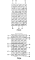
- Figures 1 shows in schematic form a display device comprising thirty five display elements 1 to 35 arranged in seven rows of five elements.
- the display elements 6 to 10 in the second row are connected to corresponding ones of the display elements 11 to 15 in the third row.
- the display elements 21 to 25 in the fifth row are connected to corresponding ones of the display elements 26 to 30 in the sixth row.
- the display elements 2 and 4 in the first row may also be connected together via a link 36.
- the display elements may be formed in any convenient manner and could be, for example, light emitting diodes, liquid crystal cells or blocks of material having faces of contrasting colours, the blocks being selectively positionable to show a desired coloured face.
- connection between the connected elements may be either a mechanical coupling when the display elements are constructed from blocks of material having contrasting coloured faces or may be electrical connections where light emitting diodes or liquid crystal cells are used.
- a possible modification to this embodiment is to make the elements of the second and third rows into elongate elements so that a single element covers both the second and third row in any position along the row. A similar arrangement may be used for rows 5 and 6.
- Figure 2 shows an alpha-numeric character set which can be displayed by appropriately energising the elements of the display device shown in Figure 1. It can be seen from Figure 2 that a recognisable character can be generated to represent each numeral from 0 to 9 and each letter of the alphabet.
- the character set shown in Figure 2 is not the only character set which could be generated using the display device of Figure 1. Various modifications could be made to individual characters particularly if the link 36 is omitted.
- each display element is square but rather the elements may be shaped to provide a more aesthetically pleasing or readable character.
- the relative sizes and spacing of the element may be changed to provide the most readable character for a given size of display device.
- Figures 3 and 4 show the electrodes and their connections in a display device of the type shown in Figure 1, in which the display elements are formed by liquid crystal cells.
- the display elements are configured as two matrices for addressing.
- the first matrix mainly corresponds to the upper half of the character while the second matrix mainly corresponds to the lower half of the character.
- Figure 3 shows the separate connections for each character while Figure 4 shows the common connections for all the display devices in a serial array.
- the upper matrix comprises elements 1 to 15, 17, 19 and 20, while the lower matrix comprises the other display elements.
- a first connection S1 is connected to electrodes la, 6a, 7a, lla, 12a and 17a;
- a second connection S2 is connected to electrodes 2a, 3a, 4a, 8a, 13a and 19a;
- a third connection S3 is connected to electrodes 5a, 9a, 10a, 14a, 15a and 20a.
- These electrodes are one electrode of the correspondingly numbered display element of Figure 1.
- connection Bl is connected to electrodes lb, 2b, 4b and 5b; a connection B2 is connected to electrodes 7b, 3b, 9b, 12b and 14b; a connection B3 is connected to electrodes 6b, llb, 13b, 8b, 15b and lOb; and a connection B4 is connected electrodes 17b, 19b and 20b.
- These electrodes form the other electrode of the liquid crystal cell which makes up the display element of the corresponding number.
- connection S4 is connected to electrodes 31a, 26a, 21a, 16a, 22a and 27a; connection S5 is connected to electrodes 33a, 32a, 28a, 23a and 18a; and connection S6 is connected to electrodes 34a, 35a, 29a, 24a, 25a and 30a.
- connection B5 is connected to electrodes 16b, 18b, 25b and 30b; connection B6 is connected to electrodes 22b, 27b, 23b, 28b, 24b and 29b; connection B7 is connected to electrodes 26b, 21b, 32b and 35b; and connection B8 is connected to electrodes 31b, 33b and 34b.
- the liquid crystals forming elements will become either transparent or opaque and hence by selectively applying appropriate signals to the connections Sl to S6 and B1 to B8 the display devices can be operated to display a desired character.
- each display device may be represented schematically as row and column conductors interconnected at each intersection by a capacitor as shown in Figures 5a and 5b.
- the reference numbers of the capacitors are the same as those of the elements which they represent.
- a series of select pulses drives each row while a series of data pulses drives each column.
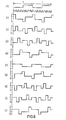
- Figures 6b, c,d and e show the waveforms of the select pulses applied to the back plane terminals Bl to B4 and B5 to B8 respectively.
- the basic waveform of period T is shown in Figure 6a. Each period T is divided in 8 sub-periods t l to t 8 .
- Each row is selected for a quarter of the period T by taking the basic waveform shown in Figure 6f and modifying it to produce a positive going pulse in the first half of the period T and a negative going pulse in the second half of the period T.
- the positive going pulses occur for 1/8 of the period T, the periods t l ,t 2 ,t 3 and t 4 corresponding to the periods of the positive going pulses for the rows Bl,B2,B3 and B4 respectively or B5,B6,B7 and B8 respectively.
- the negative going pulses also occur for 1/8 of the period T, the periods t 5 ,t 6 ,t 7 and t 8 corresponding to the periods of negative going pulses for the rows B1,B2,B3 and B4 respectively or B5,B6,B7 and B8 respectively.
- FIGs 6f to 6j Examples of data pulses which may be applied to the columns S1,S2 and S3 or S4,S5 and S6 are shown in Figures 6f to 6j.
- the waveform shown in Figure 6f will cause all the elements 1,7,12,6,11 and 17 to be off; the waveform shown in Figure 6g will cause element 1 only to switch on; the waveform shown in Figure 6h will cause elements 7 and 12 to switch on; the waveform shown in Figure 6i will cause elements 6 and 11 to switch on; and the waveform shown in Figure 6j will cause element 17 to switch on. It will be readily apparent that these waveforms shown in Figure 6f to 6j may be combined to select several of the elements simultaneously.
- the waveform shown in Figure 6f will cause all the elements 16,22,27,21,26 and 31 to be off; the waveform shown in Figure 6g will cause element 16 only to switch on; the waveform shown in Figure 6h will cause elements 22 and 27 to switch on; the waveform shown in Figure 6j will cause elements 21 and 26 to switch on;and waveform j will cause element 31 only to switch on. It will be readily apparent that these waveforms shown in Figure 6 f to j may be combined to select more than one of the elements simultaneously.
- the amplitude of the waveforms in Figures 6a to j may be as shown in the Figure.
- the liquid crystal elements are operated by a.c. signals and the contrast ratio is dependent on the RMS voltage of the a.c. signal across the element.
- the waveform shown in Figure 6 it can be derived that the RMS voltage across an element which is switched off is 1 volt and that across an element which is switched on is 1.73 volts.
- Other voltages may be used dependent on the requirements of the liquid crystals cells used.
- Figure 7 shows in block schematic form an arrangement for driving an n character display; where n is an integer, for example 16.
- a display may, for example, be used on a telephone instrument to display the number dialled or to display simple messages such as NUMBER ENGAGED.
- the arrangement shown in Figure 7 has an input terminal 100 to which input data in the form of characters to be displayed is fed.
- the input data may be in the form of a serial ASCII code which is clocked into a shift register 101 under the control of a clock signal on a line 102 which is generated in a clock signal generator 103.
- the clock signals produced by the generator 103 must either be synchronised with the input data or some means must be provided to synchronise the clock and data.
- a character When a character has been received it is fed in parallel to a decoder 104 over lines 105-1 to 105-n.
- the decoder 104 which may be in the form of a read only memory (ROM) produces outputs which are fed via an appropriate one of the lines 106-1 to 106-n to an encoder 107 which converts the decoded character into an element code which indicates which elements of the display device are to be driven to display that character.
- the encoder 107 may also be formed by a ROM and may be combined with the ROM 104 to provide the element drive code directly from the input code.
- the output of the encoder 107 is fed via lines 108-1 to 108-n and clocked into a register 109 in parallel under the control of clock signals from a clock signal generator 103 over a line 110.
- a further clock signal causes the data to be read out of the register 109 into a selected one of a plurality of registers 111-1 to 111-n, the particular register being selected by means of address signals generated in the clock generator 103 and fed to the registers 111-1 to 111-n over lines 112-1 to 112-n.
- the outputs of the register 111-1 to 111-n are fed via lines 113-1 to 113-n to inputs of respective multiplex waveform generators 114-1 to 114-n.
- the multiplex waveform generators 114-1 to 114-n are also fed with clock signals from the clock generator 103 over lines 115-1 to 115-n.
- the multiplex waveform generators 114-1 to 114-n produce three separate waveforms at three separate outputs, the three waveforms being for application to respective ones of the lines S1,S2 and S3 of each individual display device. These waveforms are fed via respective driver circuits 116-1 to 116-n to the Sl,S2 and S3 inputs of each device within a display unit l17.
- the clock pulse generator 103 is connected via a line 118 to a further multiplex waveform generator 119 which generates the four waveforms which are applied via a driver circuit 120 to lines B1,B2,B3 and B4 of the display unit 117, the lines B.1,B2,B3 and B4 of each display device in the display unit 117 being serially connected.
- the arrangement so far described up to but not including the display arrangement 117 is duplicated in the box indicated 125.
- the arrangement in box 125 produces the driving signals for the S4,S5 and S6 inputs of each of the display devices and the B5,B6,B7 and B8 lines of the display unit 117.
- block 125 produces the signals for the lower half of each character.
- the characters to be displayed are encoded and fed to the input 100 and read into the shift register 101. If the encoded characters are present in parallel form then a parallel input register will be used instead of the shift register 10.1.
- a clock signal on line 102 causes the parallel outputs of the shift register 101 to be connected to the inputs of the decoder 104 which converts the ASCII code to individual characters and causes one of the lines 106-1 to 106-n to be activated to address the encoder 107.
- the individual characters are encoded by the encoder 107 into a code which indicates which of the display elements are to be operated to form the top half of the character.
- the encoder 107 produces a 12 bit binary code for that purpose and this code is read into the register 109 under the control of clock signals from the clock signal generator 103 over the line 110.
- the output from the register 109 is fed under the control of further clocks signals on line 110 to a selected one of the registers 111-1 to 111-n, the particular register being selected by an address generated in the clock signal.generator 103.
- the registers 111-1 to 111-n will be addressed sequentially whenever information to be displayed is changed and the addresses generated will allow for the display of blank characters e.g. to mark the end of complete words.
- the address generator section of the display needs to have an indication of when a new character or set of characters is available and is/are to be displayed.
- the registers 111-1 to 111-n are only addressed when the information to be displayed is altered.
- the outputs of the register 111-1 to 111-n are connected to respective multiplex waveform generators 114-1 to 114-n which generate the waveforms required to drive the corresponding individual character display devices. These waveforms are generated with the aid of clock signals from the clock signal generator 103 which are conveyed to the multiplex waveform generators over the lines 115-1 to 115-n.
- the multiplex waveform generators produce waveforms such as those shown in Figure 6f to j, the precise waveform produced being dependent on the contents of the register 111 associated with it.
- Each multiplex waveform generator 114 produces three separate waveforms which are for application to the S1,S2 and S3 lines of its associated display device via respective driver circuits 116.
- a further multiplex waveform generator 119 generates the waveforms which are applied to the B1,B2,B3 and B4 lines of all the display devices in the display unit 117.
- the waveforms generated by the multiplex waveform generator 119 are not dependent on the character to be displayed and are generated with the aid of clock pulses fed from the clock pulse generator over line 118.
- Signals produced by the multiplex waveform generator l19 are fed to the display unit 117 via the driver circuit 120.
- the input shift register 101, decoder 104, encoder 107 and register 109 could drive both halves of the circuit separately and be common to both halves.
- the clock generator 103 may be common to both sections as may also be multiplex waveform genertor 119 and driver 120 with the Bl connection being directly connected to the B5 connection, the B2 connection beomg directly connected to the B6 connection, the B3 connection being directly connected to the B7 connection and the B4 connection being directly connected to the B8 connection.
- the register 111 could be common to both halves of the display. The actual partition will depend on the practicalities of the number of connections to the integrated circuits required in each particular case.
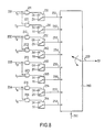
- Figure 8 shows part of one embodiment of the multiplex waveform generators 114-1 to 114-n.
- Each multiplex waveform generator comprising three of the circuits shown in Figure 8.
- the first terminal 201 is connected to the first input of an AND gate 211 and to the first input of an AND gate 221.
- the output of AND gate 211 is connected to a control input of an analogue switch 231 while the output of the gate 221 is connected to a control input of an analogue switch 241.
- the pole of switch 231 is connected to a first input 251 of a single pole eight way switch 260 while the pole of switch 241 is connected to a second input 252 of the switch 260.
- a first terminal of switch 231 is connected to OV while a second terminal is connected to 2V
- a first terminal of the switch 241 is connected to 3V while a second terminal is connected to 1V.
- three further identical arrangements are provided to which input terminals 202,203 and 204 are connected and which are connected to inputs 253 to 258 of the switch 260.
- the pole 259 of the switch 260 is the output of the multiplex waveform generator and is connected to the line Sl.
- the timing signals t l to tg are also connected to a control input 261 of the switch 260 and are operative to cause the pole 259 of the switch to be connected to selected inputs at the appropriate time, that is to input 251 during time t l to input 252 during time t 5 and so on.
- a logical '1' is applied to terminal 201 and and logical '0' to terminals 202,203 and 204.
- the AND gate 211 produces a logical '1' at its output during the time t l and causes the pole of switch 231 to be connected to OV.
- OV is applied to input 251 of the switch 260.
- the pole of 259 of switch 260 is connected to input 251 and hence OV is applied to line S1.
- the pole switch 260 is connected to inputs 253,255 and 257 in turn.
- a voltage of OV will be applied to line S1 during the period t 2 and during the period t 6 a voltage of 3V will be applied to the line Sl.
- the signal applied to terminal 203 will determine the voltages applied to line Sl during the periods t 3 and t 7 and the signal applied to terminal 204 will determine the voltages applied to the line Sl during the periods t 4 and t 8 .
- the multiplex waveform generator 119 which provides the driving waveforms shown in Figures 6b to e, produces unchanging waveforms, that is waveforms which do not change with the characters to be displayed. Consequently the multiplex waveform generator 119 receives a clock signal input but not data inputs.
- the embodiment of the multiplex waveform generator 119 shown in Figure 9 comprises four similar circuits the only difference between the circuits being the timing signals applied to them.
- the first circuit comprises two controlled single pole changeover switches 301 and 302, the switching of which is controlled by timing signals t 1 and t 5 respectively.
- the poles of switches of 301 and 302 are connected to first and second inputs of a further controlled single pole changeover switch 303, the pole of which is connected to B1.
- the control input of switch 303 is connected to the output of an RS bistable circuit 304 which is set by the timing pulse t 1 and reset by the timing pulse t 5 .
- switch 301 In operation when the pulse t 1 occurs switch 301 is set so that the movable contact connects the pole to 3V and the bistable 304 is set so that the pole of switch 303 is connected to the pole of switch 301. Consequently during the period t l 3V is applied to the line Bl. At the end of the period t l the pole of switch 301 is connected to 1V but the state of switch 303 remains unchanged and hence 1V is applied to the line Bl until the start of the period t 5 . At the start of the period t 5 the pole of switch 302 is connected to OV and the bistable 304 is reset thus causing the pole of switch 303 to be connected to switch 302. Thus during the period t 5 OV is applied to the line B1.
- the pole of switch 202 is connected to 2V but the state of switch 303 remains unchanged and hence 2V is applied to the line B1 for the periods t 6 to tg. Consequently the line Bl is at 3V during t l , 1V from t 2 to t 4 , OV during t 5 and 2V from t 6 to tg.
- switches 311,312 and 313 bistable 314 and timing pulses t 2 and t 6 produce the waveform on line B2; switches 321,322,323, bistable 341 and timing pulses t 3 and t 7 produce the waveform on B3; and switches 331,332 and 333 bistable 334 and timing pulses t 6 and tg produce the waveform on line B4.
- the clock signal generator 103 comprises an oscillator and a number of divider and decoder stages to produce the required timing and address waveforms. It is not necessary for the input data clocks, that is the clocking of the shift register 101, register 109 and registers 111-1 to 111-n, to be synchronised with the waveforms of the multiplex waveform generators.
- the clock.rate for the registers may be chosen to suit the speed of the technology chosen to implement them and the rate at which a character data is applied. Clearly if the character data is received serially the shift register 101 must be clocked at the data rate. Similarly there must be external inputs to the clock signal generator to enable the appropriate characters or registers to be reset when new display information is to be received so that the information can be routed to the appropriate display device.
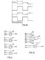
- FIGS 11 and 12 Alternative arrangements for the multiplex waveform generators 114 and 119 are illustrated in Figures 11 and 12 respectively and waveforms generated in the clock pulse generator 103 and applied to the multiplex waveform generators 114 and 119 are shown in Figure 10.
- the waveforms shown in Figure 10 comprise square waves of period T each half of the square wave is divided into four periods P O , P l , P 2 , P 3 and signals corrsponding to these periods are generated in the clock pulse generator 103 by means of appropriate divider and decoder circuits.
- the waveform shown in Figure 10a has peak amplitudes of 1V and 2V
- the waveform shown in Figure 10b has peak amplitudes of OV and 3V
- the waveform shown in Figure 10c has peak amplitudes of 1V and 2V
- the waveform shown in Figure 10d has peak amplitudes of OV and 3V.
- Figure 11 shows an alternative form for the multiplex waveform generator 119 which generates the backplane waveforms for application to the terminals Bl,B2,B3 and B4 or B5,B6,B7 and B8 of the display arrangement 117.
- the multiplex waveform generator shown in Figure 11 comprises four changeover switching arrangements 400, 401, 402, and 403, a control input of which is conected to control signal input terminals 410, 411, 412, and 413 respectively.
- the waveform shown in Figure 10a is applied to a first contact of each switching arrangement via terminals 420, 421, 422, and 423, respectively, while the waveform shown in Figure 10b is applied to a second contact of each switching arrangement via terminals 430, 431, 432, and 433 respectively.
- each switching arrangement is connected to respective output terminals 440, 441, 442, and 443 which carry the signals for application to the terminals B1,B2,B3, and B4 or B5,B6,B7, and B8 of the display arrangement 117.
- signals P 0 , P 1 , P 2 , and P 3 are applied to the respective changeover switching arrangements 400,401,402 and 403 and cause the changeover switches to change state for the periods P 0 , P 1 , P 2 and P 3 , respectively.
- the waveform shown in Figure 10b is applied to terminal 440 as the signal B1 (or B5) while the waveform shown in Figure 10a is applied to terminals 441,442, and 443.
- the waveform shown in Figure lOb is applied to terminal 441 as the signal B2 (or B6) while the waveform shown in Figure 10a is applied to the terminals 440, 442, and 443.
- the waveform shown in Figure 10b is applied to terminals 442 and 443, respectively (as signals B3 or B7 and B4 or B8) while the other terminals carry the waveform shown in Figure 10a.
- Figure 12 shows an alternative form for the waveform generator 114-n, the arrangement in Figure 12 being triplicated to form the complete waveform generator 114-n.
- the arrangement shown in Figure 12 comprises four two input AND gates 500,501,502 and 503 having respective first inputs connected to terminals 510,511,512 and 513 and respective second inputs connected to terminals 520,521,522 and 523.
- the outputs of the AND gates 500 to 503 are conected to respective inputs of a four input OR gate 530 whose output is connected to a control input of a changeover switching arrangement 531.
- First and second contacts of the changeover switching arrangement 531 are connected to respective input terminals 532 and 533 while the pole of the changeover switching arrangement 531 is connected to an output terminal 534.
- the output terminal 534 is arranged to convey the signal S1, S2, or S3 (or S4,S5 or S6) to each display device in the display arrangement 117.
- data signals D1,D2,D3, and D4 are applied to the first inputs of the AND gates 500,501,502, and 503, the data signals being derived from the register 111, while the timing signal P 0 , P 1 , P 2 , and P 3 are applied to the second inputs of the AND gates 500,501,502, and 503.
- the waveform shown in Figure lOc is applied to the terminal 532 while the waveform shown in Figure 10d is applied to the terminal 533.
- the state of the appropriate data signal will determine which of the waveforms applied to the terminals 532 and 533 will be passed to the output terminal 534. Consequently any combination of elements in the display can be selected by the application of appropriate data signals Dl to D4.
- switches shown in Figures 8, 9, 11 and 12 are in the form of solid state switches which may be take different forms depending on the technology used to produce a display arrangement, for example bipolar or MOS integrated circuits using small, medium or large scale integration. Such switching arrangements are well known to those skilled in the art.
- the form of the display devices shown in Figure 1 enables a full alpha-numeric character set to be displayed while reducing the multiplex factor that needs to be used in a matrix addressed display device. Further the display information required to be stored is reduced by approximately 30%.
- a significant overall saving in chip area can be achieved.
Landscapes
- Engineering & Computer Science (AREA)
- Chemical & Material Sciences (AREA)
- Crystallography & Structural Chemistry (AREA)
- Physics & Mathematics (AREA)
- Computer Hardware Design (AREA)
- General Physics & Mathematics (AREA)
- Theoretical Computer Science (AREA)
- Control Of Indicators Other Than Cathode Ray Tubes (AREA)
- Devices For Indicating Variable Information By Combining Individual Elements (AREA)
Applications Claiming Priority (2)
| Application Number | Priority Date | Filing Date | Title |
|---|---|---|---|
| GB08407788A GB2156566B (en) | 1984-03-26 | 1984-03-26 | Alpha-numeric display device and visual display arrangement employing such devices |
| GB8407788 | 1984-03-26 |
Publications (2)
| Publication Number | Publication Date |
|---|---|
| EP0159068A2 true EP0159068A2 (de) | 1985-10-23 |
| EP0159068A3 EP0159068A3 (de) | 1988-09-28 |
Family
ID=10558686
Family Applications (1)
| Application Number | Title | Priority Date | Filing Date |
|---|---|---|---|
| EP85200430A Withdrawn EP0159068A3 (de) | 1984-03-26 | 1985-03-20 | Alphanumerische Anzeigeeinheit und visuelle Anzeigeeinrichtung mit solchen Einheiten |
Country Status (4)
| Country | Link |
|---|---|
| EP (1) | EP0159068A3 (de) |
| JP (1) | JPS60218691A (de) |
| CA (1) | CA1257371A (de) |
| GB (1) | GB2156566B (de) |
Cited By (1)
| Publication number | Priority date | Publication date | Assignee | Title |
|---|---|---|---|---|
| US5266934A (en) * | 1989-09-28 | 1993-11-30 | U.S. Philips Corporation | Alpha-numerical display device |
Family Cites Families (5)
| Publication number | Priority date | Publication date | Assignee | Title |
|---|---|---|---|---|
| US4233602A (en) * | 1977-03-30 | 1980-11-11 | Hitachi, Ltd. | Multi-matrix display system having matrix display panel with uncrossed connections on substrates |
| US4198629A (en) * | 1977-06-06 | 1980-04-15 | General Electric Company | Numerical display using plural light sources and having a reduced and substantially constant current requirement |
| DE2757555A1 (de) * | 1977-11-30 | 1979-05-31 | Bbc Brown Boveri & Cie | Elektrooptische anzeigevorrichtung |
| EP0164152A3 (de) * | 1984-05-08 | 1986-10-08 | Koninklijke Philips Electronics N.V. | Elektrooptische Anzeigevorrichtung |
| DE59004171D1 (de) * | 1989-03-08 | 1994-02-24 | Rieter Ag Maschf | Verstelleinrichtung. |
-
1984
- 1984-03-26 GB GB08407788A patent/GB2156566B/en not_active Expired
-
1985
- 1985-03-20 EP EP85200430A patent/EP0159068A3/de not_active Withdrawn
- 1985-03-21 CA CA000477176A patent/CA1257371A/en not_active Expired
- 1985-03-25 JP JP6050985A patent/JPS60218691A/ja active Pending
Cited By (1)
| Publication number | Priority date | Publication date | Assignee | Title |
|---|---|---|---|---|
| US5266934A (en) * | 1989-09-28 | 1993-11-30 | U.S. Philips Corporation | Alpha-numerical display device |
Also Published As
| Publication number | Publication date |
|---|---|
| GB2156566B (en) | 1987-05-13 |
| GB2156566A (en) | 1985-10-09 |
| JPS60218691A (ja) | 1985-11-01 |
| GB8407788D0 (en) | 1984-05-02 |
| EP0159068A3 (de) | 1988-09-28 |
| CA1257371A (en) | 1989-07-11 |
Similar Documents
| Publication | Publication Date | Title |
|---|---|---|
| US5237314A (en) | Addressing a matrix device using electro-optical switching | |
| US4481511A (en) | Matrix display device | |
| EP0078402B1 (de) | Steuerschaltung für eine Anzeigeeinrichtung mit Anzeigeelementen in Form einer Matrix | |
| US3787834A (en) | Liquid crystal display system | |
| US4386351A (en) | Method and system for two-dimensional traveling display and driver circuits therefor | |
| US4113361A (en) | Liquid crystal display device | |
| GB1267179A (de) | ||
| US7746306B2 (en) | Display device having an improved video signal drive circuit | |
| US4356483A (en) | Matrix drive system for liquid crystal display | |
| KR100832666B1 (ko) | 화상 표시 장치 및 그 구동 방법 | |
| US4206459A (en) | Numeral display device | |
| US20080018639A1 (en) | Apparatus for Driving Matrix-Type Lcd Panels and a Liquid Crystal Display Based Thereon | |
| EP0109713A2 (de) | Alphanumerische Anzeigevorrichtung und Sichtanzeigeanordnung mit solchen Anzeigevorrichtungen | |
| US3848250A (en) | Optical character-displaying apparatus using liquid crystals | |
| CA1257371A (en) | Alpha-numeric display device and visual display arrangement employing such devices | |
| US4288792A (en) | Electronic apparatus with time-division drive | |
| US4392131A (en) | Integratable activation module for passive electrooptical displays | |
| KR20000035327A (ko) | 디지탈화상신호 입력대응 구동회로내장형 액정표시장치 | |
| US4262292A (en) | Multiplexed scan display circuit | |
| EP0544427B1 (de) | Steuerschaltung für eine Anzeigeeinheit mit digitaler Sourcesteuerung zur Erzeugung von Mehrfachpegelsteuerspannungen aus einer einzelnen externen Energiequelle | |
| EP0067365A1 (de) | Matrixanzeigeeinrichtung | |
| KR20050038648A (ko) | 액티브 매트릭스 디스플레이 구동 | |
| KR100328897B1 (ko) | 표시용마이크로컴퓨터 | |
| KR100313349B1 (ko) | 보조 펄스를 이용한 다중 어드레싱 | |
| JP2569476B2 (ja) | 液晶駆動表示方式 |
Legal Events
| Date | Code | Title | Description |
|---|---|---|---|
| PUAI | Public reference made under article 153(3) epc to a published international application that has entered the european phase |
Free format text: ORIGINAL CODE: 0009012 |
|
| AK | Designated contracting states |
Designated state(s): CH DE FR GB LI SE |
|
| RAP3 | Party data changed (applicant data changed or rights of an application transferred) |
Owner name: N.V. PHILIPS' GLOEILAMPENFABRIEKEN Owner name: PHILIPS ELECTRONIC AND ASSOCIATED INDUSTRIES LIMIT |
|
| PUAL | Search report despatched |
Free format text: ORIGINAL CODE: 0009013 |
|
| AK | Designated contracting states |
Kind code of ref document: A3 Designated state(s): CH DE FR GB LI SE |
|
| 17P | Request for examination filed |
Effective date: 19890320 |
|
| STAA | Information on the status of an ep patent application or granted ep patent |
Free format text: STATUS: THE APPLICATION HAS BEEN WITHDRAWN |
|
| 18W | Application withdrawn |
Withdrawal date: 19910506 |
|
| R18W | Application withdrawn (corrected) |
Effective date: 19910506 |
|
| RIN1 | Information on inventor provided before grant (corrected) |
Inventor name: MULKERRIN, ROBERT ANTHONY Inventor name: PHILIPS, IAN |