EP0159601A2 - Arrangement de circuit logique à transistors à effet de champ d'une construction adaptée à cet arrangement - Google Patents
Arrangement de circuit logique à transistors à effet de champ d'une construction adaptée à cet arrangement Download PDFInfo
- Publication number
- EP0159601A2 EP0159601A2 EP85104166A EP85104166A EP0159601A2 EP 0159601 A2 EP0159601 A2 EP 0159601A2 EP 85104166 A EP85104166 A EP 85104166A EP 85104166 A EP85104166 A EP 85104166A EP 0159601 A2 EP0159601 A2 EP 0159601A2
- Authority
- EP
- European Patent Office
- Prior art keywords
- electrode layer
- circuit arrangement
- gate
- layer
- charge
- Prior art date
- Legal status (The legal status is an assumption and is not a legal conclusion. Google has not performed a legal analysis and makes no representation as to the accuracy of the status listed.)
- Withdrawn
Links
Images

Classifications
-
- H—ELECTRICITY
- H10—SEMICONDUCTOR DEVICES; ELECTRIC SOLID-STATE DEVICES NOT OTHERWISE PROVIDED FOR
- H10D—INORGANIC ELECTRIC SEMICONDUCTOR DEVICES
- H10D30/00—Field-effect transistors [FET]
- H10D30/60—Insulated-gate field-effect transistors [IGFET]
- H10D30/68—Floating-gate IGFETs
- H10D30/681—Floating-gate IGFETs having only two programming levels
Definitions
- the invention relates to a logic circuit arrangement with the features of the preamble of claim 1.
- Logic circuit arrangements are used for digital and analog data processing, to which a multitude of requirements are placed.
- a logic circuit with high packing density i.e. for highly integrated circuits (VLSI).
- VLSI highly integrated circuits
- Such a circuit should have a high processing speed.
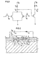
- FIG. 1 shows an example of a circuit (which is known per se) which is suitable here and which has a NOR gate and a subsequent inverter stage. This circuit is operated with a supply voltage V DD . It is desirable that such a circuit be operated with only a single polarity with regard to both the supply voltage and the drive voltages to be provided for the elements.
- field-effect transistors of the normally-off type ie of the enhancement type, which are not conductive without a gate voltage.
- V el , V e2 positive gate voltages
- these transistors are turned on or by the corresponding lowering of the potential V al , the transistor of the inverter stage turns off.
- a gallium arsenide field effect transistor with an extremely thin, active gallium arsenide layer is known. Further details can be found in "1979 GaAs IC Symposium, Lake Tahoe, Sept. 1979". Such a field-effect transistor is blocking without an applied gate voltage and becomes conductive with a gate voltage. Problems with such field-effect transistors arise in connection with the integration, because namely, over a larger chip area, such a small thickness of the active layer is difficult to maintain within the limits that are acceptable with respect to tolerable fluctuations in the threshold voltage value. Another disadvantage is the unfavorable working range in the unsaturated part of the characteristic field at low operating voltages, which means that for a fiction appropriate circuit steepness and high switching speed would not be achieved here.
- junction field-effect transistors which have a pn diode instead of the Schottky gate mentioned and whose logic voltage swing is increased by a few tenths of a volt.
- high marginal capacitance in the p-range leads to severe switching delays.
- isolation gate field effect transistors whose thin insulating layer below the Schottky gate serves to avoid the high forward currents of a Schottky field effect transistor that occur when the gate voltage is applied positively. Thickness of the insulating layer which is not exactly observed results in large fluctuations in the threshold voltage value.
- Another known field-effect transistor of the normally-off type is the HEMT transistor with a very thin (50 nm) layer of highly doped gallium aluminum arsenide below the Schottky gate and with an intentionally undoped, active gallium arsenide layer.
- a logic circuit with direct coupling of successive transistors, e.g. 1 to realize with normally-off transistors of the above types leads to problems already shown.
- logic circuits with normally-on field-effect transistors should also be mentioned.
- this includes depletion MESFET field-effect transistors.
- These have, for example, 150 nm thick active layer of, for example, gallium arsenide on an electrically insulating substrate, for example of preferably semi-insulating gallium arsenide.
- active layer of gallium arsenide on an electrically insulating substrate, for example of preferably semi-insulating gallium arsenide.
- Such transistors in integrated circuits have relatively little differences in the threshold voltage value from one another. They also have a relatively short switching time and high immunity to interference.
- Their main disadvantage is that they require a gate voltage opposite to the supply voltage V DD in order to be switched non-conductive. This requires an additional power supply. This also creates additional switching delays and power loss.
- the object of the present invention is to provide measures which can be used to implement a logic circuit arrangement which has the advantages of known technologies but is free from their disadvantages.
- the circuit arrangement according to the invention should be such that, on the one hand, it has high switching speed, low power dissipation, high driver strength, while at the same time minimizing the technological production effort, and which does not require any further voltage source.
- the fluctuation of the threshold voltage values should be as small as possible with reasonable technological effort.
- a field-effect transistor adapted for a logic circuit arrangement has been developed for the present invention, the details of which are described in more detail below.
- the field-effect transistor used in the invention has features of its construction which are known in principle from field-effect transistors of various types.
- the substrate the active semiconductor layer located on the substrate, the source region and contact, the drain region and contact as well as with respect to the gate electrode, general knowledge of field effect transistors can be pointed out.
- the field-effect transistor has insulator material between the active semiconductor layer and the gate electrode, in which an adhesive layer in the form of an electrically conductive electrode layer is embedded parallel to the expansion of the gate electrode or the active semiconductor layer.
- an adhesive layer in the form of an electrically conductive electrode layer is embedded parallel to the expansion of the gate electrode or the active semiconductor layer.
- the use of such an electrode layer arranged in this way is known per se, for example as a floating gate.
- 4,441,036 disclose a semiconductor structure which can be referred to as a field effect transistor and which has a polysilicon layer parallel to it in the interior of an insulator layer below a gate electrode. This layer also has no external contact.
- This field-effect transistor known from the aforementioned DE-OS or US-PS is intended to be fuseable link in a circuit with redundant circuit elements or circuit groups. By charging this electrode layer made of polysilicon by means of electron beam embossed from the outside, this known switching element can be changed in the manufacture of the circuit arrangement in which it is used so that it is subsequently continuously conductive or permanently blocking, that is to say it produces a permanent electrical connection to a circuit part or maintains a continuous interruption.
- MNOS field effect transistors which are used as programmable memory elements in particular. You can have an electrode that cannot be connected to the outside between the oxide and nitride layers.
- the respective storage state is set or changed by applying overvoltages and by tunnel current of charge carriers through the oxide and / or nitride layer, for which purpose this only has a small thickness, e.g. smaller than 10 nm.
- the invention provides for the manufacture of the circuit arrangement according to the invention, i.e. of the field effect transistors provided according to the invention with the features already specified, to charge the trap or electrode layer in such a way that this field effect transistor of the normally-on type becomes effective as one of the normally-off type.
- This can be controlled by the normal control of its gate or the gate electrode from the (in the absence of gate voltage) blocking state to the (in the presence of gate voltage) conducting state, this being reversible as desired.
- this adhesive layer or electrode layer is permanently charged in a surface-specific manner (equal to or higher than that) in accordance with the following condition (1):
- ⁇ h is the dielectric constant of the semiconductor material of the active layer
- ⁇ i is the dielectric constant of the trap or. Insulator material surrounding the electrode layer
- d i the distance of the gate electrode from the surface of the active semiconductor layer
- d! the distance of the electrode layer from the gate electrode (the thickness of the electrode layer is negligible)
- d is the thickness of the active semiconductor layer
- N D is, the doping of the active semiconductor layer having a donor for n-type (or acceptors for p-type) transistor
- w the width of the source / drain contact
- ⁇ min the difference in work function (in volts) between the metal of the gate electrode and the semiconductor material).
- the charge to be applied Q HSS (Cb / cm 2 ) on the electrode layer is negative for n-type transistors and positive for p-type transistors. (Slightly) higher charging, in particular 10 to 20% higher charging, results in higher threshold voltage with a correspondingly higher level of interference immunity.
- L is the length over which the (trap) electrode layer extends between the source region and the drain region (with their spacing L K ) of the transistor according to the invention.
- the elementary charge is designated by e.
- the distance di is preferably chosen to be equal to half the distance d i , ie the electrode layer is arranged at least approximately in the middle between the surface of the active semiconductor layer and the gate electrode.
- FIG. 2. 1 denotes the substrate made of insulating, semi-insulating or complementary to the active semiconductor layer 2 doped material, the substrate material preferably being semiconductor material.
- a source contact 3 and a drain contact 4 are provided, which in the example shown are arranged on the surface of the active semiconductor layer 2. There are no locks de contacts.
- the gate electrode 8 extends over the length Lg as the control electrode of the transistor. According to an embodiment variant, this gate electrode 8 is embedded in the material of an insulator layer.
- This insulator layer consists of the parts labeled 5, 7 and 9. It contains the adhesion point or electrode layer 6.
- This electrode layer 6, preferably of the same length L, is electrically insulated from the surface of the active layer 2 by the portion forming the insulating layer 5.
- the portion forming the insulating layer 7 insulates the electrode layer 6 from the gate electrode 8. The distances resulting from the layer thicknesses are shown with d i and di.
- the gate electrode 8 and the electrode layer 6 are preferably dimensioned and arranged to cover one another.
- the electrode layer 6 may also be (somewhat) shorter and / or (somewhat) narrower, but is to be placed covered by the gate electrode 8.
- An important peculiarity of the invention is that here the gate electrode does not have to reach the source / drain regions and certainly does not have to overlap.
- This is namely known for MOS field-effect transistors in which a thin oxide layer is provided for electrical isolation between the gate electrode on the one hand and the source / drain regions on the other hand. Since a corresponding distance can be provided in the invention, the field oxides areas 9 possible, ensure safe insulation for the corresponding adjacent electrodes. That this peculiarity of the invention is possible at all is due to the fact that the one or more transistors with a forced normally-off property used in a circuit arrangement according to the invention have this only in the range (over the length L) which is equal to the corresponding extension of the Adhesive layer or electrode layer 6.
- the (lateral in FIG. 2) distance between the electrode layer 6 on the one hand and the source / drain region 3/4 on the other hand be approximately at least as large as or greater than the layer thickness, namely the insulation distance between the electrode layer 6 and the gate electrode 8 or Semiconductor layer 2 to choose.
- a technologically uncritical dimensioning of eg 150 nm with a doping of eg 10 17 cm -3 can, as is usual for MES field-effect transistors of the opposite type (depletion type).
- Layers 5 and 7 also have a manageably large thickness (greater than or equal to 50 nm).
- a directly coupled logic circuit arrangement can be realized which manages with only one supply voltage V DD and whose fluctuations in the threshold voltages of individual transistors according to the invention are negligibly small.
- the field-effect transistor used in the invention is produced by method steps which are known per se and using materials which are customarily used.
- the semiconductor material of layer 2 can be silicon, for example. Indium phosphide, gallium arsenide, gallium indium arsenide etc. are also suitable. In particular, compound semiconductor material is of interest for the invention.
- Drain / source contacts can be N + regions with contact metallization thereon. For example, a 5 nm thick metal or semiconductor layer is provided as the electrode layer 6, which is, for example, 500 nm long and 10 pm wide.
- the thickness d i of the insulator layer 7 (and the layer 5) is, for example, 50 nm and it consists of, for example, silicon dioxide, silicon nitride, aluminum oxide or the like. Corresponding material is used for the field oxide 9. Charging the detention or. Electrode layer 6 takes place with masking, for example a photoresist layer. The same applies to the gate electrode 8. In addition, in a manner known per se, the conductor tracks connecting the drain gate and source regions (of the transistors of the circuit arrangement) are applied to the surface.
- the transistor has normally-off behavior, so that direct coupling to upstream and downstream stages without additional circuitry and can be done with only one supply voltage V DD .
- Another advantage is that in the invention, such a uniformity of the active layer 2 can be maintained over a large chip area that only results in small fluctuations in the value of the threshold voltage.
- Another important advantage is the possibility of using a complementary transistor as a load resistor (see also FIG.
- the charge carrier transport is not the same as with the other normally-off transistors (enrichment and inversion types) Insulator-semiconductor interface, where the mobility is reduced due to the interface roughness, but takes place in the undisturbed semiconductor volume.
- the density of the energy states in the energy gap at the insulator / semiconductor interface should also be kept small in the new logic, so that any charge carriers sitting in these states do not cause "Fermini level pinning". This condition can be met by particularly clean manufacturing process management, as has already been shown for silicon MOSFETs and GalnAs, InP and GaAs MISFETs.
- the interlayer state density reaches a value comparable to the charge Q HSS , the charge calculated according to equation (1) must be increased by the value of the interlayer state density.
- FIG. 3 is a complementary circuit, already mentioned, with a trough 14 which has the opposite substrate type 1 to the opposite conductivity type.
- the reference symbols used in FIG. 3 have the meanings given for FIG. 2.
- the reference numerals provided with the addition a have the corresponding meaning, but are related to the complementary transistor implemented in the well 14.
- An embodiment according to FIG. 3 can be implemented in particular in silicon technology. In this implementation of a complementary circuit according to the invention, apart from the switching current, practically no current flows.
- FIG. 4 shows a microwave amplifier.
- the signal 15 to be amplified is applied to the gate 8 via the capacitor 16, which blocks the gate bias voltage 12.
- the inductor 17 leads the gate bias voltage 12 to the gate 8 and keeps the signal of the signal generator 15 from remote from the battery 12.
- the amplified signal is passed from drain 4 via capacitor 18 to load impedance 19.
- the DC direct voltage 11 is fed to the drain contact 4 via the inductance 20.
- the advantage of this circuit lies in its simplicity because of the same polarities of the batteries 11 and 12, which can be replaced by a single supply voltage. This favors monolithic integration ("MIC") and increases the cutoff frequency compared to normally-on MESFET circuits.
- the other reference numerals correspond to those in FIG. 2.
- This circuit works as an analog amplifier or with an additional feedback to be provided as a self-oscillating oscillator (the signal generator 15 can be omitted).
Landscapes
- Logic Circuits (AREA)
- Metal-Oxide And Bipolar Metal-Oxide Semiconductor Integrated Circuits (AREA)
- Design And Manufacture Of Integrated Circuits (AREA)
Applications Claiming Priority (2)
| Application Number | Priority Date | Filing Date | Title |
|---|---|---|---|
| AT1194/84 | 1984-04-10 | ||
| AT119484 | 1984-04-10 |
Publications (2)
| Publication Number | Publication Date |
|---|---|
| EP0159601A2 true EP0159601A2 (fr) | 1985-10-30 |
| EP0159601A3 EP0159601A3 (fr) | 1987-08-19 |
Family
ID=3508644
Family Applications (1)
| Application Number | Title | Priority Date | Filing Date |
|---|---|---|---|
| EP85104166A Withdrawn EP0159601A3 (fr) | 1984-04-10 | 1985-04-04 | Arrangement de circuit logique à transistors à effet de champ d'une construction adaptée à cet arrangement |
Country Status (3)
| Country | Link |
|---|---|
| US (1) | US4713676A (fr) |
| EP (1) | EP0159601A3 (fr) |
| JP (1) | JPS60259021A (fr) |
Families Citing this family (5)
| Publication number | Priority date | Publication date | Assignee | Title |
|---|---|---|---|---|
| JPH05207442A (ja) * | 1992-01-30 | 1993-08-13 | Matsushita Electric Ind Co Ltd | 動画像信号の符号化装置 |
| US6884093B2 (en) | 2000-10-03 | 2005-04-26 | The Trustees Of Princeton University | Organic triodes with novel grid structures and method of production |
| US7345915B2 (en) * | 2005-10-31 | 2008-03-18 | Hewlett-Packard Development Company, L.P. | Modified-layer EPROM cell |
| TW200935751A (en) * | 2008-02-04 | 2009-08-16 | Mediatek Inc | Sample-and-hold amplifiers |
| FR3062517B1 (fr) | 2017-02-02 | 2019-03-15 | Soitec | Structure pour application radiofrequence |
Family Cites Families (5)
| Publication number | Priority date | Publication date | Assignee | Title |
|---|---|---|---|---|
| GB1329220A (en) * | 1969-08-11 | 1973-09-05 | California Inst Of Techn | Stored charge device |
| US4467453A (en) * | 1979-09-04 | 1984-08-21 | Texas Instruments Incorporated | Electrically programmable floating gate semiconductor memory device |
| US4334347A (en) * | 1979-10-19 | 1982-06-15 | Rca Corporation | Method of forming an improved gate member for a gate injected floating gate memory device |
| DE3032306A1 (de) * | 1980-08-27 | 1982-04-08 | Siemens AG, 1000 Berlin und 8000 München | Monolithisch integrierte schaltung mit zu- und/oder abschaltbaren schaltungsteilen |
| JPS58158972A (ja) * | 1982-03-16 | 1983-09-21 | Toshiba Corp | 半導体装置の製造方法 |
-
1985
- 1985-04-04 EP EP85104166A patent/EP0159601A3/fr not_active Withdrawn
- 1985-04-10 US US06/721,797 patent/US4713676A/en not_active Expired - Fee Related
- 1985-04-10 JP JP60076315A patent/JPS60259021A/ja active Pending
Also Published As
| Publication number | Publication date |
|---|---|
| EP0159601A3 (fr) | 1987-08-19 |
| JPS60259021A (ja) | 1985-12-21 |
| US4713676A (en) | 1987-12-15 |
Similar Documents
| Publication | Publication Date | Title |
|---|---|---|
| DE112014003481B4 (de) | GaN-TRANSISTOREN MIT POLYSILIZIUMSCHICHTEN ZUR BILDUNG VON ZUSÄTZLICHEN KOMPONENTEN UND VERFAHREN ZU DEREN HERSTELLUNG | |
| DE69324871T2 (de) | Hochspannungs-MIS-Feldeffektransistor und integrierte Halbleiterschaltung | |
| DE2312414C2 (de) | Verfahren zur Herstellung von integrierten MOSFET-Schaltkreisen | |
| DE2706623C2 (fr) | ||
| DE2537564C2 (de) | Verfahren zur Herstellung einer integrierten Schaltung sowie Verwendung dieses Verfahrens | |
| DE1918222C3 (de) | Isolierschicht-Feldeffekttransistor | |
| DE2619663B2 (de) | Feldeffekttransistor, Verfahren zu seinem Betrieb und Verwendung als schneller Schalter sowie in einer integrierten Schaltung | |
| EP0833386A1 (fr) | Dispositif semiconducteur vertical contrÔlable par effet de champ | |
| DE2231933B2 (de) | Festkörperschalter | |
| DE3145230A1 (de) | "halbleiteranordnung" | |
| DE102016111036B4 (de) | Schaltkreis und Verfahren zum Betreiben des Schaltkreises | |
| DE1965340A1 (de) | Schottky-Diode | |
| DE2531846C2 (de) | Schutzschaltungsanordnung für einen Isolierschicht-Feldeffekttransistor | |
| DE102016105908A1 (de) | High-Electron-Mobility-Transistor (HEM-Transistor) mit einem in eine Gatestruktur integrierten RC-Netzwerk | |
| DE3125470C2 (fr) | ||
| DE102017210711A1 (de) | Halbleiterbauelement | |
| EP0217065B1 (fr) | Circuit intégré en technique complémentaire comportant un générateur de polarisation de substrat | |
| DE19644821C1 (de) | Steuerbare Halbleiterstruktur mit verbesserten Schalteigenschaften | |
| EP0071916B1 (fr) | Transistor à effet de champ MOS de puissance et procédé de sa fabrication | |
| DE3882304T2 (de) | Mikrowellentransistor mit Doppelheteroübergang. | |
| DE3750310T2 (de) | Heteroübergangs-Feldeffektanordnung. | |
| DE112022001954T5 (de) | Halbleitervorrichtung, verfahren zum herstellen der halbleitervorrichtung und leistungsumsetzungsvorrichtung | |
| DE4228832C2 (de) | Feldeffekt-gesteuertes Halbleiterbauelement | |
| DE102020000633A1 (de) | Elektronische vorrichtung mit einem halbleiterkörper oder einer isolationsstruktur in einem graben | |
| EP0159601A2 (fr) | Arrangement de circuit logique à transistors à effet de champ d'une construction adaptée à cet arrangement |
Legal Events
| Date | Code | Title | Description |
|---|---|---|---|
| PUAI | Public reference made under article 153(3) epc to a published international application that has entered the european phase |
Free format text: ORIGINAL CODE: 0009012 |
|
| AK | Designated contracting states |
Designated state(s): AT DE FR GB IT |
|
| 17P | Request for examination filed |
Effective date: 19850827 |
|
| PUAL | Search report despatched |
Free format text: ORIGINAL CODE: 0009013 |
|
| AK | Designated contracting states |
Kind code of ref document: A3 Designated state(s): AT DE FR GB IT |
|
| 17Q | First examination report despatched |
Effective date: 19880622 |
|
| STAA | Information on the status of an ep patent application or granted ep patent |
Free format text: STATUS: THE APPLICATION IS DEEMED TO BE WITHDRAWN |
|
| 18D | Application deemed to be withdrawn |
Effective date: 19890413 |