EP0159869B1 - Composition céramique diélectrique pour condensateurs multicouches - Google Patents
Composition céramique diélectrique pour condensateurs multicouches Download PDFInfo
- Publication number
- EP0159869B1 EP0159869B1 EP85302561A EP85302561A EP0159869B1 EP 0159869 B1 EP0159869 B1 EP 0159869B1 EP 85302561 A EP85302561 A EP 85302561A EP 85302561 A EP85302561 A EP 85302561A EP 0159869 B1 EP0159869 B1 EP 0159869B1
- Authority
- EP
- European Patent Office
- Prior art keywords
- pbo
- mgo
- dielectric
- ceramic material
- sintering aid
- Prior art date
- Legal status (The legal status is an assumption and is not a legal conclusion. Google has not performed a legal analysis and makes no representation as to the accuracy of the status listed.)
- Expired
Links
Images


Classifications
-
- C—CHEMISTRY; METALLURGY
- C04—CEMENTS; CONCRETE; ARTIFICIAL STONE; CERAMICS; REFRACTORIES
- C04B—LIME, MAGNESIA; SLAG; CEMENTS; COMPOSITIONS THEREOF, e.g. MORTARS, CONCRETE OR LIKE BUILDING MATERIALS; ARTIFICIAL STONE; CERAMICS; REFRACTORIES; TREATMENT OF NATURAL STONE
- C04B35/00—Shaped ceramic products characterised by their composition; Ceramics compositions; Processing powders of inorganic compounds preparatory to the manufacturing of ceramic products
-
- C—CHEMISTRY; METALLURGY
- C04—CEMENTS; CONCRETE; ARTIFICIAL STONE; CERAMICS; REFRACTORIES
- C04B—LIME, MAGNESIA; SLAG; CEMENTS; COMPOSITIONS THEREOF, e.g. MORTARS, CONCRETE OR LIKE BUILDING MATERIALS; ARTIFICIAL STONE; CERAMICS; REFRACTORIES; TREATMENT OF NATURAL STONE
- C04B35/00—Shaped ceramic products characterised by their composition; Ceramics compositions; Processing powders of inorganic compounds preparatory to the manufacturing of ceramic products
- C04B35/01—Shaped ceramic products characterised by their composition; Ceramics compositions; Processing powders of inorganic compounds preparatory to the manufacturing of ceramic products based on oxide ceramics
- C04B35/495—Shaped ceramic products characterised by their composition; Ceramics compositions; Processing powders of inorganic compounds preparatory to the manufacturing of ceramic products based on oxide ceramics based on vanadium, niobium, tantalum, molybdenum or tungsten oxides or solid solutions thereof with other oxides, e.g. vanadates, niobates, tantalates, molybdates or tungstates
- C04B35/497—Shaped ceramic products characterised by their composition; Ceramics compositions; Processing powders of inorganic compounds preparatory to the manufacturing of ceramic products based on oxide ceramics based on vanadium, niobium, tantalum, molybdenum or tungsten oxides or solid solutions thereof with other oxides, e.g. vanadates, niobates, tantalates, molybdates or tungstates based on solid solutions with lead oxides
-
- H—ELECTRICITY
- H01—ELECTRIC ELEMENTS
- H01G—CAPACITORS; CAPACITORS, RECTIFIERS, DETECTORS, SWITCHING DEVICES, LIGHT-SENSITIVE OR TEMPERATURE-SENSITIVE DEVICES OF THE ELECTROLYTIC TYPE
- H01G4/00—Fixed capacitors; Processes of their manufacture
- H01G4/002—Details
- H01G4/018—Dielectrics
- H01G4/06—Solid dielectrics
- H01G4/08—Inorganic dielectrics
- H01G4/12—Ceramic dielectrics
- H01G4/1209—Ceramic dielectrics characterised by the ceramic dielectric material
- H01G4/1254—Ceramic dielectrics characterised by the ceramic dielectric material based on niobium or tungsteen, tantalum oxides or niobates, tantalates
Definitions
- the present invention is related to ceramic compositions having a high dielectric constant and high insulation resistance at temperatures up to 85°C and which are capable of being formed by sintering a mixture of oxides at relatively low temperatures in the range of about 900 to 1050°C. More particularly, the present invention is directed to ceramic compositions particularly suited for use as the dielectric in multilayer ceramic capacitors.
- Ceramic compositions using barium titanate have been used successfully as the dielectric materials for ceramic capacitors; however, such compositions require relatively high sintering temperatures e.g. 1200°C and higher, and this precludes the use of relatively inexpensive metal, such as silver and nickel, as capacitor electrodes, and mandates the use of higher melting, expensive precious metals, such as platinum.
- lead oxide-based perovskite dielectric systems have been proposed to achieve low sintering temperatures while providing a relatively high dielectric constant and insulation resistance, for example, US ⁇ A ⁇ 4.,216,102 to Furukawa et al.
- Such prior art lead oxide-based solid solution systems provide significant advantages, however, there remains the need to provide high dielectric constants with increased temperature dependence stability and higher insulation resistance at high temperatures, more comparable to barium titanate base dielectrics.
- a lead oxide-base dielectric ceramic material having a dielectric constant of at least 10,000 at 25°C and 10000 (+22% to -56%) over the temperature range of 10-85°C and insulation resistance of at least 10 12 ohm-cm at 25°C and 10 11 ohm-cm at 85°C which is formed from a sintered mixture of oxide powders and has a microstructure comprising a predominantly lead perovskite solid solution phase surrounding small discrete regions of metal oxide residues, said ceramic material comprising by weight,
- the present invention further provides a method of forming a lead-oxide based dielectric ceramic material which comprises:
- the ceramic composition used in the present invention is characterised by being sinterable at temperatures in the range of 900 to 1050°C and providing a dielectric constant (K) of at least 10,000 at 25°C and 10,000 (+22% to -56%) over the range of 10-85°C and insulation resistance of at least 10" ohm-cm at 25°C and 10 11 ohm-cm at 85°C.
- K dielectric constant
- the relative low PbO content is particularly important to the achievement of high dielectric constant as are the relationships recited with respect to Pb, Fe, Mg and Nb.
- the relatively minor amounts of Mn0 2 and of the sintering aid additives enables optimum densification of the dielectric, and enhance the insulation resistance, especially at high temperatures (e.g. 85°C). Further, these additives in combination result in the insulation resistance remaining high during capacitor life testing under high temperature and voltage stresses.
- a blended mixture of finely divided particles of PbO, MgO, Fe 2 0 3 and Nb 2 0 s is provided in appropriate proportions and manganese, e.g. in the form of a manganese-containing salt such as manganous nitrate or acetate, is added to provide the desired Mn0 2 content in the sintered ceramic, and the mixture is calcined at about 720 to 780°C for about 60 to 180 minutes in an air atmosphere.
- the resulting calcine material is milled to a size of about 0.6 micronmeter and blended with finely divided (e.g. -1 micronmeter) oxide sintering aid additive, in the amount of about 1-3% by weight of the calcine.
- Suitable sintering aid materials include Pb 5 Ge 1.95 Si 1.05 O 11 , (melting point 720°C, resistivity >1013 ohm-cm) and lead-containing glasses such as compositions A and B in Table A, below.
- the mixture thus obtained is sintered at 900 to 1050°C for about 60 to 180 minutes in the course of which the calcine and the sintering aid constituents react to provide a reaction product characterised by a microstructure comprising a predominantly lead perovskite solid solution phase surrounding discrete regions of sintering aid metal oxide residues.
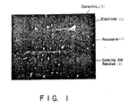
- a representative microstructure (original magnification 750x) is shown in Figure 1.
- the microstructure shown in Figure 1 was determined using scanning electron microscopy.
- the chemical compositions of the phases, to the degree that they were determined, were analysed by energy-dispersive X-ray analysis.
- the crystal structure of the major phase (perovskite) was determined by X-ray diffraction.
- 1 indicates generally the dielectric composition of the invention, and 2 is a capacitor electrode typically made of silver containing 5 to 25 wt.% palladium.
- the lead-containing perovskite phase of the dielectric composition is indicated at 3.
- the dark regions 4 surrounded by the perovskite dielectric phase 3 are sintering aid metal oxide residues, Si0 2 and Ge0 2 .
- Ceramic dielectric material in accordance with the present invention is used as the dielectric for multilayer ceramic capacitors following conventional practice and using relatively inexpensive metals such as silver and its alloys as the electrode material.
- a calcine material was prepared from the following:
- the materials were milled, dried and calcined at 750°C, for 120 minutes.
- Mn(N0 3 ) 2 was added to the mixture before calcining to provide a desired Mn0 2 content in the calcine and, in further instances, oxidic sintering aid material was added after calcining to provide a desired sintering aid content.
- the multilayer capacitors had individual dielectric layers of about 1.2 mils (30.5 ⁇ m) thickness and a total capacitance of about 1 microfarad (for a dielectric constant of 10,000).
- Samples A-H not in accordance with the present invention, reflect the known behavior of lead magnesium iron niobate as described in US-A-4,216,102 and elsewhere in the prior art. That is, as the PbO content approaches the stoichiometric value of about 68.25 wt.% for the dielectric constant and the insulation resistance of the material both increase sharply (Samples A-H as shown in Figures 2(a)-(c) and Table (II).
- Sample I was made generally in accord with the present invention, but with an incorrect ratio of Pb/Nb+Mg+Fe.
- Mn0 2 compare series E-H with A-D
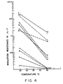
- the compositions of this invention exhibit a high dielectric constant and very high insulation resistance at a significantly substoichiometric PbO content, at which other formulations exhibit low dielectric constants and very low insulation resistances, particularly at high temperatures, as can be seen in Figures 2(c) and Figure 4.
- Figure 4 is a graph showing insulation resistance as a function of temperature for the materials of the example. As can be seen, the materials J, K, L in accordance with the present invention are superior.
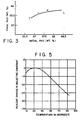
- Figure 5 is a graph showing dielectric constant change with temperature for materials in accordance with the present invention.
- a significant aspect of the formulations of this invention is the manner in which they can be sintered.
- the usual practice is to sinter PbO containing perovskites in closed crucibles often with lead-containing "atmosphere powders" near the bodies to minimize lead loss.
- sintering can be accomplished in open containers such as those used to make barium titanate multilayer capacitors, using an excess of PbO.
- PbO loss from the dielectric during sintering results in the achievement of the desired PbO content.
- Figure 3 shows the PbO content for the presintered mixture and sintered compositions for samples J, K, L of the present invention.
- a relatively wide range of initial high PbO contents results in a narrow range of final composition in accordance with the present invention.
Landscapes
- Engineering & Computer Science (AREA)
- Chemical & Material Sciences (AREA)
- Ceramic Engineering (AREA)
- Manufacturing & Machinery (AREA)
- Organic Chemistry (AREA)
- Structural Engineering (AREA)
- Materials Engineering (AREA)
- Power Engineering (AREA)
- Inorganic Chemistry (AREA)
- Microelectronics & Electronic Packaging (AREA)
- Compositions Of Oxide Ceramics (AREA)
- Inorganic Insulating Materials (AREA)
- Ceramic Capacitors (AREA)
- Fixed Capacitors And Capacitor Manufacturing Machines (AREA)
Claims (4)
Applications Claiming Priority (2)
| Application Number | Priority Date | Filing Date | Title |
|---|---|---|---|
| US59997784A | 1984-04-13 | 1984-04-13 | |
| US599977 | 1984-04-13 |
Publications (3)
| Publication Number | Publication Date |
|---|---|
| EP0159869A2 EP0159869A2 (fr) | 1985-10-30 |
| EP0159869A3 EP0159869A3 (en) | 1986-01-29 |
| EP0159869B1 true EP0159869B1 (fr) | 1988-09-07 |
Family
ID=24401885
Family Applications (1)
| Application Number | Title | Priority Date | Filing Date |
|---|---|---|---|
| EP85302561A Expired EP0159869B1 (fr) | 1984-04-13 | 1985-04-12 | Composition céramique diélectrique pour condensateurs multicouches |
Country Status (5)
| Country | Link |
|---|---|
| EP (1) | EP0159869B1 (fr) |
| JP (1) | JPH0610929B2 (fr) |
| KR (1) | KR890002694B1 (fr) |
| CA (1) | CA1255891A (fr) |
| DE (1) | DE3564800D1 (fr) |
Families Citing this family (2)
| Publication number | Priority date | Publication date | Assignee | Title |
|---|---|---|---|---|
| JP2666388B2 (ja) * | 1988-07-11 | 1997-10-22 | 株式会社村田製作所 | 積層セラミックコンデンサ |
| CN101295635B (zh) * | 2007-04-29 | 2010-05-19 | 中芯国际集成电路制造(上海)有限公司 | 改善mim电容容量的方法及装置 |
Family Cites Families (4)
| Publication number | Priority date | Publication date | Assignee | Title |
|---|---|---|---|---|
| US4027209A (en) * | 1975-10-02 | 1977-05-31 | Sprague Electric Company | Ceramic capacitor having a silver doped dielectric of (Pb,La)(Zr,Ti)O3 |
| FR2519970B1 (fr) * | 1982-01-18 | 1985-12-06 | Centre Nat Rech Scient | Ceramiques a haute constante dielectrique, procede pour leur obtention et leur application aux condensateurs multicouches |
| US4379319A (en) * | 1982-02-18 | 1983-04-05 | Ferro Corporation | Monolithic ceramic capacitors and improved ternary ceramic compositions for producing same |
| GB2126575B (en) * | 1982-08-03 | 1985-11-13 | Standard Telephones Cables Ltd | Ceramic capacitors and dielectric compositions |
-
1985
- 1985-04-10 CA CA000478750A patent/CA1255891A/fr not_active Expired
- 1985-04-12 DE DE8585302561T patent/DE3564800D1/de not_active Expired
- 1985-04-12 JP JP60076851A patent/JPH0610929B2/ja not_active Expired - Lifetime
- 1985-04-12 EP EP85302561A patent/EP0159869B1/fr not_active Expired
- 1985-04-12 KR KR1019850002449A patent/KR890002694B1/ko not_active Expired
Also Published As
| Publication number | Publication date |
|---|---|
| EP0159869A3 (en) | 1986-01-29 |
| EP0159869A2 (fr) | 1985-10-30 |
| DE3564800D1 (de) | 1988-10-13 |
| JPH0610929B2 (ja) | 1994-02-09 |
| CA1255891A (fr) | 1989-06-20 |
| JPS60232607A (ja) | 1985-11-19 |
| KR890002694B1 (ko) | 1989-07-24 |
| KR850007239A (ko) | 1985-12-02 |
Similar Documents
| Publication | Publication Date | Title |
|---|---|---|
| EP0087004B1 (fr) | Composition céramique et condensateur obtenu avec cette composition céramique | |
| US5097391A (en) | Ceramic multilayer chip capacitor and method for making | |
| EP0534378B1 (fr) | Composition céramique diélectrique non-réductible | |
| EP0690462B1 (fr) | Condensateur céramique multicouche et son procédé de fabrication | |
| US4309295A (en) | Grain boundary barrier layer ceramic dielectrics and the method of manufacturing capacitors therefrom | |
| KR100203928B1 (ko) | 모놀리틱 세라믹 커패시터 및 이의 제조 방법 | |
| EP0350770B1 (fr) | Composition céramique semi-conductrice | |
| US4459364A (en) | Low-fire ceramic dielectric compositions | |
| EP0180132B1 (fr) | Composition céramique à constante diélectrique élevée | |
| US4882652A (en) | High dielectric constant type ceramic composition | |
| US4550088A (en) | Ceramic composition for dielectric in multilayer capacitors | |
| EP0159869B1 (fr) | Composition céramique diélectrique pour condensateurs multicouches | |
| US4985381A (en) | Dielectric ceramic composition | |
| GB2027008A (en) | Ceramic Dielectrics | |
| JPH06208806A (ja) | 誘電体材料およびセラミック部品 | |
| US4499521A (en) | Low-fire ceramic dielectric compositions for multilayer ceramic capacitors | |
| EP0413321A1 (fr) | Composition céramique diélectrique et condensateur à couche multiple | |
| JP3469910B2 (ja) | 誘電体磁器組成物 | |
| US6136739A (en) | High dielectric ceramic capacitor composition | |
| JP3469911B2 (ja) | 誘電体磁器組成物 | |
| JPH06208804A (ja) | 誘電体材料およびセラミック部品 | |
| GB2031398A (en) | High dielectric cosntant type ceramic composition | |
| JPH0794022A (ja) | 誘電体材料およびセラミック部品 | |
| JPH06349330A (ja) | 誘電体材料およびセラミック部品 | |
| JPH0883514A (ja) | 誘電体磁器組成物 |
Legal Events
| Date | Code | Title | Description |
|---|---|---|---|
| PUAI | Public reference made under article 153(3) epc to a published international application that has entered the european phase |
Free format text: ORIGINAL CODE: 0009012 |
|
| AK | Designated contracting states |
Designated state(s): DE FR GB |
|
| PUAL | Search report despatched |
Free format text: ORIGINAL CODE: 0009013 |
|
| AK | Designated contracting states |
Designated state(s): DE FR GB |
|
| 17P | Request for examination filed |
Effective date: 19860224 |
|
| 17Q | First examination report despatched |
Effective date: 19870212 |
|
| GRAA | (expected) grant |
Free format text: ORIGINAL CODE: 0009210 |
|
| AK | Designated contracting states |
Kind code of ref document: B1 Designated state(s): DE FR GB |
|
| REF | Corresponds to: |
Ref document number: 3564800 Country of ref document: DE Date of ref document: 19881013 |
|
| ET | Fr: translation filed | ||
| PLBE | No opposition filed within time limit |
Free format text: ORIGINAL CODE: 0009261 |
|
| 26N | No opposition filed | ||
| REG | Reference to a national code |
Ref country code: GB Ref legal event code: IF02 |
|
| PGFP | Annual fee paid to national office [announced via postgrant information from national office to epo] |
Ref country code: GB Payment date: 20020416 Year of fee payment: 18 |
|
| PGFP | Annual fee paid to national office [announced via postgrant information from national office to epo] |
Ref country code: FR Payment date: 20020423 Year of fee payment: 18 |
|
| PGFP | Annual fee paid to national office [announced via postgrant information from national office to epo] |
Ref country code: DE Payment date: 20020430 Year of fee payment: 18 |
|
| PG25 | Lapsed in a contracting state [announced via postgrant information from national office to epo] |
Ref country code: GB Free format text: LAPSE BECAUSE OF NON-PAYMENT OF DUE FEES Effective date: 20030412 |
|
| PG25 | Lapsed in a contracting state [announced via postgrant information from national office to epo] |
Ref country code: DE Free format text: LAPSE BECAUSE OF NON-PAYMENT OF DUE FEES Effective date: 20031101 |
|
| GBPC | Gb: european patent ceased through non-payment of renewal fee |
Effective date: 20030412 |
|
| PG25 | Lapsed in a contracting state [announced via postgrant information from national office to epo] |
Ref country code: FR Free format text: LAPSE BECAUSE OF NON-PAYMENT OF DUE FEES Effective date: 20031231 |
|
| REG | Reference to a national code |
Ref country code: FR Ref legal event code: ST |