EP0160220A1 - Dispositif pour gravure au plasma - Google Patents
Dispositif pour gravure au plasma Download PDFInfo
- Publication number
- EP0160220A1 EP0160220A1 EP85103878A EP85103878A EP0160220A1 EP 0160220 A1 EP0160220 A1 EP 0160220A1 EP 85103878 A EP85103878 A EP 85103878A EP 85103878 A EP85103878 A EP 85103878A EP 0160220 A1 EP0160220 A1 EP 0160220A1
- Authority
- EP
- European Patent Office
- Prior art keywords
- wafer
- electrode
- holder
- recess
- holders
- Prior art date
- Legal status (The legal status is an assumption and is not a legal conclusion. Google has not performed a legal analysis and makes no representation as to the accuracy of the status listed.)
- Granted
Links
Images

Classifications
-
- H—ELECTRICITY
- H10—SEMICONDUCTOR DEVICES; ELECTRIC SOLID-STATE DEVICES NOT OTHERWISE PROVIDED FOR
- H10P—GENERIC PROCESSES OR APPARATUS FOR THE MANUFACTURE OR TREATMENT OF DEVICES COVERED BY CLASS H10
- H10P72/00—Handling or holding of wafers, substrates or devices during manufacture or treatment thereof
- H10P72/70—Handling or holding of wafers, substrates or devices during manufacture or treatment thereof for supporting or gripping
- H10P72/76—Handling or holding of wafers, substrates or devices during manufacture or treatment thereof for supporting or gripping using mechanical means, e.g. clamps or pinches
- H10P72/7604—Handling or holding of wafers, substrates or devices during manufacture or treatment thereof for supporting or gripping using mechanical means, e.g. clamps or pinches the wafers being placed on a susceptor, stage or support
- H10P72/7611—Handling or holding of wafers, substrates or devices during manufacture or treatment thereof for supporting or gripping using mechanical means, e.g. clamps or pinches the wafers being placed on a susceptor, stage or support characterised by edge profile or support profile
-
- H—ELECTRICITY
- H10—SEMICONDUCTOR DEVICES; ELECTRIC SOLID-STATE DEVICES NOT OTHERWISE PROVIDED FOR
- H10P—GENERIC PROCESSES OR APPARATUS FOR THE MANUFACTURE OR TREATMENT OF DEVICES COVERED BY CLASS H10
- H10P72/00—Handling or holding of wafers, substrates or devices during manufacture or treatment thereof
- H10P72/04—Apparatus for manufacture or treatment
- H10P72/0402—Apparatus for fluid treatment
- H10P72/0418—Apparatus for fluid treatment for etching
- H10P72/0421—Apparatus for fluid treatment for etching for drying etching
-
- H—ELECTRICITY
- H10—SEMICONDUCTOR DEVICES; ELECTRIC SOLID-STATE DEVICES NOT OTHERWISE PROVIDED FOR
- H10P—GENERIC PROCESSES OR APPARATUS FOR THE MANUFACTURE OR TREATMENT OF DEVICES COVERED BY CLASS H10
- H10P72/00—Handling or holding of wafers, substrates or devices during manufacture or treatment thereof
- H10P72/10—Handling or holding of wafers, substrates or devices during manufacture or treatment thereof using carriers specially adapted therefor, e.g. front opening unified pods [FOUP]
- H10P72/18—Handling or holding of wafers, substrates or devices during manufacture or treatment thereof using carriers specially adapted therefor, e.g. front opening unified pods [FOUP] characterised by being specially adapted for supporting a single substrate or by comprising a stack of such individual supports
-
- H—ELECTRICITY
- H10—SEMICONDUCTOR DEVICES; ELECTRIC SOLID-STATE DEVICES NOT OTHERWISE PROVIDED FOR
- H10P—GENERIC PROCESSES OR APPARATUS FOR THE MANUFACTURE OR TREATMENT OF DEVICES COVERED BY CLASS H10
- H10P72/00—Handling or holding of wafers, substrates or devices during manufacture or treatment thereof
- H10P72/70—Handling or holding of wafers, substrates or devices during manufacture or treatment thereof for supporting or gripping
- H10P72/76—Handling or holding of wafers, substrates or devices during manufacture or treatment thereof for supporting or gripping using mechanical means, e.g. clamps or pinches
- H10P72/7604—Handling or holding of wafers, substrates or devices during manufacture or treatment thereof for supporting or gripping using mechanical means, e.g. clamps or pinches the wafers being placed on a susceptor, stage or support
- H10P72/7618—Handling or holding of wafers, substrates or devices during manufacture or treatment thereof for supporting or gripping using mechanical means, e.g. clamps or pinches the wafers being placed on a susceptor, stage or support characterised by a movable susceptor, stage or support, others than those only rotating on their own vertical axis, e.g. susceptors on a rotating carrousel
-
- H—ELECTRICITY
- H10—SEMICONDUCTOR DEVICES; ELECTRIC SOLID-STATE DEVICES NOT OTHERWISE PROVIDED FOR
- H10P—GENERIC PROCESSES OR APPARATUS FOR THE MANUFACTURE OR TREATMENT OF DEVICES COVERED BY CLASS H10
- H10P72/00—Handling or holding of wafers, substrates or devices during manufacture or treatment thereof
- H10P72/70—Handling or holding of wafers, substrates or devices during manufacture or treatment thereof for supporting or gripping
- H10P72/76—Handling or holding of wafers, substrates or devices during manufacture or treatment thereof for supporting or gripping using mechanical means, e.g. clamps or pinches
- H10P72/7604—Handling or holding of wafers, substrates or devices during manufacture or treatment thereof for supporting or gripping using mechanical means, e.g. clamps or pinches the wafers being placed on a susceptor, stage or support
- H10P72/7621—Handling or holding of wafers, substrates or devices during manufacture or treatment thereof for supporting or gripping using mechanical means, e.g. clamps or pinches the wafers being placed on a susceptor, stage or support characterised by supporting two or more semiconductor substrates
-
- H—ELECTRICITY
- H10—SEMICONDUCTOR DEVICES; ELECTRIC SOLID-STATE DEVICES NOT OTHERWISE PROVIDED FOR
- H10P—GENERIC PROCESSES OR APPARATUS FOR THE MANUFACTURE OR TREATMENT OF DEVICES COVERED BY CLASS H10
- H10P72/00—Handling or holding of wafers, substrates or devices during manufacture or treatment thereof
- H10P72/70—Handling or holding of wafers, substrates or devices during manufacture or treatment thereof for supporting or gripping
- H10P72/76—Handling or holding of wafers, substrates or devices during manufacture or treatment thereof for supporting or gripping using mechanical means, e.g. clamps or pinches
- H10P72/7604—Handling or holding of wafers, substrates or devices during manufacture or treatment thereof for supporting or gripping using mechanical means, e.g. clamps or pinches the wafers being placed on a susceptor, stage or support
- H10P72/7624—Handling or holding of wafers, substrates or devices during manufacture or treatment thereof for supporting or gripping using mechanical means, e.g. clamps or pinches the wafers being placed on a susceptor, stage or support characterised by the mechanical construction of the susceptor, stage or support
Definitions
- the present invention relates generally to plasma etching apparatus and more particularly to an improved plasma etching apparatus electrode structure.
- Plasma etching techniques have been widely used for etching products such as semiconductor wafers. Basically such a technique comprises the exposing of wafers to a plasma to remove surface materials, such as silicon oxide, carried on the semiconductor wafer surface. These plasma etching techniques are used in the semiconductor industry because the plasma etching process involves low temperatures. Low temperatures are realized because the power required to generate the plasma is low. Because the process uses low temperatures the use of photoresist as a mask material is permitted. Also, because plasma etching is fundamentally a chemical process, selectivity in etching is very high and mask erosion can be made minimal.
- the difficulty with such etching is non-uniformity of the species forming the plasma with respect to the material being treated. This is caused, in part by electrical field variations between the cathode and the anode.
- the products to be etched are batch etched, that is they are evenly spaced upon one electrode of the plasma etching machine and exposed to the plasma. Because large numbers of wafers can be treated at once in such batch etchers they are the preferred production etching tool even though the poor uniformity realized in such tools requires considerable tradeoffs in device size, tolerances, etc.
- batch etching increases the throughput it has been found that because of the gas flow, temperature, electric fields, plasma formation, etc. in the usual apparatus the plasma affects each wafer, in the batch, differently depending on its location in the apparatus.
- the rate of and amount of etching realized by each wafer depends significantly on the wafers position on the electrode. In general, the etching rate varies with the radial position of the wafer on the electrode. Thus batch etched wafers are non-uniformly etched.
- each of the wafer carrying electrode tailored product holders is tailored, with respect to its geographic location on the electrode, so that the characteristics of the plasma, immediately surrounding each product contained in the holder, is modified to be substantially identical to that surrounding any other product contained in any other holder.
- each holder can be tailored to compensate not only for the differences in its geographical location on the electrode but can be tailored to compensate for film abnormalities such as film thickness differences that may be on the surface of the product in the holder. Individual treatment of each of the wafers to be etched can be provided.
- the present invention solves the uniformity problems encountered in the past by forming the electrode of the apparatus with a plurality of apertures into which a plurality of product holders can be inserted.
- the electrode can be either the anode or the cathode of the apparatus.
- These holders assure both good electrical and thermal contact to the product contained therein but are also designed to physically modify the characteristics of the plasma within the vicinity of the holder.
- the holder configuration can also be altered to take into consideration the type of film being removed as well as the geographic location of the holders within the reactor.
- a cross sectional view of a typical batch type, parallel plasma etcher is shown.
- plasma etchers comprise a chamber 10 containing an upper electrode 11, and a lower electrode 12 which is carrying a plurality of semiconductor wafers 13.
- electrode 11 is the cathode and electrode 12 is the anode and both are coupled to an R-F source (not shown).
- a plasma forming gas is introduced via tube 14 through the center of cathode 11 into the chamber 10 and between the electrodes 11 and 12. With such a gas in the chamber 11 a plasma is formed between the electrodes 11 and 12 when the RF source is turned on.
- Plasma forming gas is extracted from the chamber 10 via outlet tube 9 which is coupled to a vacuum pump;(not shown).
- etching apparatus is presently commercially available and need not be further discussed.
- FIG. 1 shows a chamber with a top gas inlet and a bottom outlet that side inlet and outlet chambers can also be used.
- the anode 12 of Fig. 1, designed in accordance with the present invention, is shown in greater detail in Figs. 2 and 3.
- Fig. 2 a top view of the anode is shown.
- This anode typically, when designed for use with semiconductor wafers about 9.53 cm in diameter, comprises a substantially flat circular plate, about 0.64 cm in thickness, having a diameter of about 66.04 cm.
- the electrode 12 as shown in Fig. 2, has a plurality of apertures therein. These apertures are arranged in arrays, usually as a series of concentric rings. In the electrode shown, a central aperture 15 is surrounded by two concentric rings of apertures 15a and 15b respectively. All of these apertures are identical to one another and each has a stepped inner wall as especially shown in Fig. 3. The larger diameter 16 of the aperture is approximately 9.53 cm while the smaller diameter 17 is about 8.26 cm. Thus a 0.64 cm shoulder 18 is provided for in each aperture.
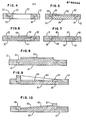
- Fig. 4 illustrates a holder formed as a ring 30 with an exterior extended lip 31 and an inner recessed shoulder 32 which supports a wafer 33.
- the wafer 33 is supported so that its upper surface is in the plane of the upper surface of the holder 30.
- the lip 31 is of suitable thickness and shape to mate with the shoulder 18 of the electrode 12 so as to support the ring 30 in any one of the apertures 15, 15a or 15b in electrode 12 so that the upper surface of the ring 30 is in the plane of the surface of the electrode 12.
- each of the holders shown in Figs. 4, 5, 6, and 7 could be modified so that the lip extends above the surface of the plane of the electrode.
- Fig. 8 shows a mesa type holder.
- This holder comprises a central body 51 provided with an extended lip 52 which rests on the shoulder 18 in the electrode 12.
- the body 51 is of such a thickness that it extends above the plane of the upper surface of the electrode 12 as a mesa and thus supports the wafer 53 above the plane of the upper surface of the electrode 12.
- Fig. 9 shows a holder that comprises a recessed dish 61 provided with an exterior rim 62 and a central recess 63 into which a wafer 64 can be inserted.
- the central recess 63 is provided with a flat bottom parallel to the upper surface of the electrode 12.
- the lip 62 is provided with an upwardly extending rim of variable thickness.
- Fig. 10 shows a variation of the beveled holder of Fig. 9.
- the wafer holder 65 is provided with an extended lip 66 and a central recess 67 into which a wafer 69 can be inserted.
- the central recess 67 has a flat bottom 68 set at an angle with respect to the upper surface of the electrode 12.
- the lip 62 is provided with a rim of variable thickness. Again by varying the thickness of the rim from one side of the holder to the other, the plane of the upper surface of the rim is again at an angle with the plane of the upper surface of the electrode 12.
- the bottom of the recess 67 is maintained at the same angle as the plane of the upper surface of the rim 66 with respect to the surface of the electrode 12 and slightly below the surface of the rim.
- Wafer uniformity means that uniformity measured using 5 points per wafer and with the result published as 3 sigma/x information.
- the holder design of Fig. 6 is used to solve both effects 1 and 2 above.
- Another added feature of the design shown in Fig. 6 is, by decreasing the depth of the recess 43 the wafer 44 the etch rate across the whole wafer is increased slightly and by deepening the recess, the etch rate of the wafer is decreased.
- the wafer is not recessed but instead is raised above the surface of the electrode by the mesa configured holder, as shown in Fig. 8, the outside edge of the wafer 53 will etch faster. With this knowledge one can populate an entire electrode with holders having different depths of recess or different height of mesa for improved batch uniformity.
- the holder design of Fig. 7 can especially be used to improve center etch rates due to better RF coupling in this region, this corrects effect number 2.
- the holder design of Fig. 5 is used to increase etch rate on the outer edge of the wafer due to better RF coupling, thus curing effect number 1.
- Both of these holder designs are susceptible to heat transfer problems. The areas of the wafer not contacting the thermally conductive pedestal tend to heat up during the etch causing some films to etch at different rates. This can be corrected by adding a heat transfer medium, which insulates electrically, to these areas of the wafer.
- the holder designs shown in Fig. 9 and 10 are best used to correct effects number 3 and number 4 above. Usually these effects are brought on by effects from the electrode edge. These edge effects generally cause the portion of the wafer closest to the electrode edge to etch faster than the remainder of the wafer.
- the rim of the pedestal is raised higher on one side than the other, usually about 0.89 cm, one can compensate for the edge effect.
- the holder is preferably positioned in the electrode so that the high side of the rim will be closest to the outermost electrode edge, thereby protecting the outside edge of the wafer more.
- the holder design, shown in Fig. 9, keeps the wafer surface parallel with the electrode surface.
- RIE reactive ion etching
- the holders can either be coated with or formed of an insulating material to improve uniformity of the etching of.the wafer.
- a holder of volatile substance chosen so that it etches at the same rate as the wafer film assists in correcting effect number 2 described above.
- this invention teaches that by using an apertured electrode and placing in the apertures product holders of selected designs that uniform etching of the product can be realized regardless of the product position in the apparatus.
- each holder controls the etching uniformity of the product contained therein by altering the local physical characteristics immediately surrounding the product contained in the holder.
- the local characteristics around each product is modified according to its own particular needs by suitable design of the holder.
Landscapes
- Drying Of Semiconductors (AREA)
- ing And Chemical Polishing (AREA)
Applications Claiming Priority (2)
| Application Number | Priority Date | Filing Date | Title |
|---|---|---|---|
| US06/596,189 US4512841A (en) | 1984-04-02 | 1984-04-02 | RF Coupling techniques |
| US596189 | 1990-10-12 |
Publications (3)
| Publication Number | Publication Date |
|---|---|
| EP0160220A1 true EP0160220A1 (fr) | 1985-11-06 |
| EP0160220B1 EP0160220B1 (fr) | 1989-05-31 |
| EP0160220B2 EP0160220B2 (fr) | 1992-08-19 |
Family
ID=24386313
Family Applications (1)
| Application Number | Title | Priority Date | Filing Date |
|---|---|---|---|
| EP85103878A Expired EP0160220B2 (fr) | 1984-04-02 | 1985-03-31 | Dispositif pour gravure au plasma |
Country Status (4)
| Country | Link |
|---|---|
| US (1) | US4512841A (fr) |
| EP (1) | EP0160220B2 (fr) |
| JP (1) | JPS60208836A (fr) |
| DE (1) | DE3570805D1 (fr) |
Cited By (4)
| Publication number | Priority date | Publication date | Assignee | Title |
|---|---|---|---|---|
| US6051503A (en) * | 1996-08-01 | 2000-04-18 | Surface Technology Systems Limited | Method of surface treatment of semiconductor substrates |
| US6187685B1 (en) | 1997-08-01 | 2001-02-13 | Surface Technology Systems Limited | Method and apparatus for etching a substrate |
| US6261962B1 (en) | 1996-08-01 | 2001-07-17 | Surface Technology Systems Limited | Method of surface treatment of semiconductor substrates |
| US6417013B1 (en) | 1999-01-29 | 2002-07-09 | Plasma-Therm, Inc. | Morphed processing of semiconductor devices |
Families Citing this family (335)
| Publication number | Priority date | Publication date | Assignee | Title |
|---|---|---|---|---|
| US4647361A (en) * | 1985-09-03 | 1987-03-03 | International Business Machines Corporation | Sputtering apparatus |
| JPH01200629A (ja) * | 1988-02-04 | 1989-08-11 | Nec Corp | ドライエッチング装置 |
| US5262029A (en) * | 1988-05-23 | 1993-11-16 | Lam Research | Method and system for clamping semiconductor wafers |
| US5511799A (en) | 1993-06-07 | 1996-04-30 | Applied Materials, Inc. | Sealing device useful in semiconductor processing apparatus for bridging materials having a thermal expansion differential |
| GB9317170D0 (en) * | 1993-08-18 | 1993-10-06 | Applied Vision Ltd | Improvements in physical vapour deposition apparatus |
| US5498313A (en) * | 1993-08-20 | 1996-03-12 | International Business Machines Corp. | Symmetrical etching ring with gas control |
| JPH08153682A (ja) * | 1994-11-29 | 1996-06-11 | Nec Corp | プラズマcvd装置 |
| US5639334A (en) * | 1995-03-07 | 1997-06-17 | International Business Machines Corporation | Uniform gas flow arrangements |
| JP2001230235A (ja) * | 2000-02-14 | 2001-08-24 | Matsushita Electric Ind Co Ltd | 水晶板のプラズマエッチング装置および水晶板の製造方法並びに水晶板 |
| JP2004193632A (ja) * | 2004-03-22 | 2004-07-08 | Matsushita Electric Ind Co Ltd | 水晶板のプラズマエッチング装置 |
| DE102004053906A1 (de) * | 2004-11-05 | 2006-05-11 | Leica Microsystems Semiconductor Gmbh | Adaptervorrichtung für eine Substrat-Arbeitsstation |
| US7431797B2 (en) * | 2006-05-03 | 2008-10-07 | Applied Materials, Inc. | Plasma reactor with a dynamically adjustable plasma source power applicator |
| US7520999B2 (en) * | 2006-05-03 | 2009-04-21 | Applied Materials, Inc. | Method of processing a workpiece in a plasma reactor with dynamic adjustment of the plasma source power applicator and the workpiece relative to one another |
| US7419551B2 (en) * | 2006-05-03 | 2008-09-02 | Applied Materials, Inc. | Plasma reactor with apparatus for dynamically adjusting the plasma source power applicator and the workpiece relative to one another |
| US7504041B2 (en) * | 2006-05-03 | 2009-03-17 | Applied Materials, Inc. | Method of processing a workpiece in a plasma reactor employing a dynamically adjustable plasma source power applicator |
| US8557093B2 (en) | 2007-03-22 | 2013-10-15 | Sunpower Corporation | Deposition system with electrically isolated pallet and anode assemblies |
| DE102007023970A1 (de) * | 2007-05-23 | 2008-12-04 | Aixtron Ag | Vorrichtung zum Beschichten einer Vielzahl in dichtester Packung auf einem Suszeptor angeordneter Substrate |
| US8962101B2 (en) | 2007-08-31 | 2015-02-24 | Novellus Systems, Inc. | Methods and apparatus for plasma-based deposition |
| JP5094307B2 (ja) * | 2007-09-25 | 2012-12-12 | 株式会社アルバック | プラズマ処理装置 |
| US8062472B2 (en) * | 2007-12-19 | 2011-11-22 | Applied Materials, Inc. | Method of correcting baseline skew by a novel motorized source coil assembly |
| US20090162570A1 (en) * | 2007-12-19 | 2009-06-25 | Applied Materials, Inc. | Apparatus and method for processing a substrate using inductively coupled plasma technology |
| US8137463B2 (en) * | 2007-12-19 | 2012-03-20 | Applied Materials, Inc. | Dual zone gas injection nozzle |
| US8999106B2 (en) * | 2007-12-19 | 2015-04-07 | Applied Materials, Inc. | Apparatus and method for controlling edge performance in an inductively coupled plasma chamber |
| EP2338164A4 (fr) * | 2008-08-29 | 2012-05-16 | Veeco Instr Inc | Support de plaquettes à résistance thermique variable |
| US9394608B2 (en) | 2009-04-06 | 2016-07-19 | Asm America, Inc. | Semiconductor processing reactor and components thereof |
| KR20120131194A (ko) * | 2010-02-24 | 2012-12-04 | 비코 인스트루먼츠 인코포레이티드 | 온도 분포 제어를 이용한 처리 방법 및 장치 |
| TWI452163B (zh) * | 2010-04-08 | 2014-09-11 | 鴻海精密工業股份有限公司 | 鍍膜治具 |
| US8535445B2 (en) * | 2010-08-13 | 2013-09-17 | Veeco Instruments Inc. | Enhanced wafer carrier |
| TWI450330B (zh) * | 2010-11-25 | 2014-08-21 | C Sun Mfg Ltd | 電漿蝕刻設備、晶圓治具及設置晶圓的方法 |
| US20120164834A1 (en) * | 2010-12-22 | 2012-06-28 | Kevin Jennings | Variable-Density Plasma Processing of Semiconductor Substrates |
| US20130023129A1 (en) | 2011-07-20 | 2013-01-24 | Asm America, Inc. | Pressure transmitter for a semiconductor processing environment |
| DE102011055061A1 (de) | 2011-11-04 | 2013-05-08 | Aixtron Se | CVD-Reaktor bzw. Substrathalter für einen CVD-Reaktor |
| KR101928356B1 (ko) * | 2012-02-16 | 2018-12-12 | 엘지이노텍 주식회사 | 반도체 제조 장치 |
| US10316412B2 (en) | 2012-04-18 | 2019-06-11 | Veeco Instruments Inc. | Wafter carrier for chemical vapor deposition systems |
| US9088085B2 (en) | 2012-09-21 | 2015-07-21 | Novellus Systems, Inc. | High temperature electrode connections |
| US10714315B2 (en) | 2012-10-12 | 2020-07-14 | Asm Ip Holdings B.V. | Semiconductor reaction chamber showerhead |
| US20160376700A1 (en) | 2013-02-01 | 2016-12-29 | Asm Ip Holding B.V. | System for treatment of deposition reactor |
| US9273413B2 (en) | 2013-03-14 | 2016-03-01 | Veeco Instruments Inc. | Wafer carrier with temperature distribution control |
| US10167571B2 (en) | 2013-03-15 | 2019-01-01 | Veeco Instruments Inc. | Wafer carrier having provisions for improving heating uniformity in chemical vapor deposition systems |
| US11015245B2 (en) | 2014-03-19 | 2021-05-25 | Asm Ip Holding B.V. | Gas-phase reactor and system having exhaust plenum and components thereof |
| US10858737B2 (en) | 2014-07-28 | 2020-12-08 | Asm Ip Holding B.V. | Showerhead assembly and components thereof |
| US10941490B2 (en) | 2014-10-07 | 2021-03-09 | Asm Ip Holding B.V. | Multiple temperature range susceptor, assembly, reactor and system including the susceptor, and methods of using the same |
| KR20170086637A (ko) * | 2014-11-26 | 2017-07-26 | 폰 아르데네 게엠베하 | 기판 유지 장치, 기판 이송 장치, 처리 조립체 및 기판 처리 방법 |
| US10276355B2 (en) | 2015-03-12 | 2019-04-30 | Asm Ip Holding B.V. | Multi-zone reactor, system including the reactor, and method of using the same |
| US10458018B2 (en) | 2015-06-26 | 2019-10-29 | Asm Ip Holding B.V. | Structures including metal carbide material, devices including the structures, and methods of forming same |
| US10211308B2 (en) | 2015-10-21 | 2019-02-19 | Asm Ip Holding B.V. | NbMC layers |
| US11139308B2 (en) | 2015-12-29 | 2021-10-05 | Asm Ip Holding B.V. | Atomic layer deposition of III-V compounds to form V-NAND devices |
| US10529554B2 (en) | 2016-02-19 | 2020-01-07 | Asm Ip Holding B.V. | Method for forming silicon nitride film selectively on sidewalls or flat surfaces of trenches |
| US10343920B2 (en) | 2016-03-18 | 2019-07-09 | Asm Ip Holding B.V. | Aligned carbon nanotubes |
| US10190213B2 (en) | 2016-04-21 | 2019-01-29 | Asm Ip Holding B.V. | Deposition of metal borides |
| US10367080B2 (en) | 2016-05-02 | 2019-07-30 | Asm Ip Holding B.V. | Method of forming a germanium oxynitride film |
| US11453943B2 (en) | 2016-05-25 | 2022-09-27 | Asm Ip Holding B.V. | Method for forming carbon-containing silicon/metal oxide or nitride film by ALD using silicon precursor and hydrocarbon precursor |
| US10612137B2 (en) | 2016-07-08 | 2020-04-07 | Asm Ip Holdings B.V. | Organic reactants for atomic layer deposition |
| US9859151B1 (en) | 2016-07-08 | 2018-01-02 | Asm Ip Holding B.V. | Selective film deposition method to form air gaps |
| KR102532607B1 (ko) | 2016-07-28 | 2023-05-15 | 에이에스엠 아이피 홀딩 비.브이. | 기판 가공 장치 및 그 동작 방법 |
| US9812320B1 (en) | 2016-07-28 | 2017-11-07 | Asm Ip Holding B.V. | Method and apparatus for filling a gap |
| US9887082B1 (en) | 2016-07-28 | 2018-02-06 | Asm Ip Holding B.V. | Method and apparatus for filling a gap |
| US10643826B2 (en) | 2016-10-26 | 2020-05-05 | Asm Ip Holdings B.V. | Methods for thermally calibrating reaction chambers |
| US11532757B2 (en) | 2016-10-27 | 2022-12-20 | Asm Ip Holding B.V. | Deposition of charge trapping layers |
| US10714350B2 (en) | 2016-11-01 | 2020-07-14 | ASM IP Holdings, B.V. | Methods for forming a transition metal niobium nitride film on a substrate by atomic layer deposition and related semiconductor device structures |
| KR102546317B1 (ko) | 2016-11-15 | 2023-06-21 | 에이에스엠 아이피 홀딩 비.브이. | 기체 공급 유닛 및 이를 포함하는 기판 처리 장치 |
| KR102762543B1 (ko) | 2016-12-14 | 2025-02-05 | 에이에스엠 아이피 홀딩 비.브이. | 기판 처리 장치 |
| US11581186B2 (en) | 2016-12-15 | 2023-02-14 | Asm Ip Holding B.V. | Sequential infiltration synthesis apparatus |
| US11447861B2 (en) | 2016-12-15 | 2022-09-20 | Asm Ip Holding B.V. | Sequential infiltration synthesis apparatus and a method of forming a patterned structure |
| KR102700194B1 (ko) | 2016-12-19 | 2024-08-28 | 에이에스엠 아이피 홀딩 비.브이. | 기판 처리 장치 |
| US10269558B2 (en) | 2016-12-22 | 2019-04-23 | Asm Ip Holding B.V. | Method of forming a structure on a substrate |
| US10867788B2 (en) | 2016-12-28 | 2020-12-15 | Asm Ip Holding B.V. | Method of forming a structure on a substrate |
| US11390950B2 (en) | 2017-01-10 | 2022-07-19 | Asm Ip Holding B.V. | Reactor system and method to reduce residue buildup during a film deposition process |
| US10468261B2 (en) | 2017-02-15 | 2019-11-05 | Asm Ip Holding B.V. | Methods for forming a metallic film on a substrate by cyclical deposition and related semiconductor device structures |
| US10529563B2 (en) | 2017-03-29 | 2020-01-07 | Asm Ip Holdings B.V. | Method for forming doped metal oxide films on a substrate by cyclical deposition and related semiconductor device structures |
| KR102457289B1 (ko) | 2017-04-25 | 2022-10-21 | 에이에스엠 아이피 홀딩 비.브이. | 박막 증착 방법 및 반도체 장치의 제조 방법 |
| US10770286B2 (en) | 2017-05-08 | 2020-09-08 | Asm Ip Holdings B.V. | Methods for selectively forming a silicon nitride film on a substrate and related semiconductor device structures |
| US10892156B2 (en) | 2017-05-08 | 2021-01-12 | Asm Ip Holding B.V. | Methods for forming a silicon nitride film on a substrate and related semiconductor device structures |
| KR102417931B1 (ko) * | 2017-05-30 | 2022-07-06 | 에이에스엠 아이피 홀딩 비.브이. | 기판 지지 장치 및 이를 포함하는 기판 처리 장치 |
| US10886123B2 (en) | 2017-06-02 | 2021-01-05 | Asm Ip Holding B.V. | Methods for forming low temperature semiconductor layers and related semiconductor device structures |
| US12040200B2 (en) | 2017-06-20 | 2024-07-16 | Asm Ip Holding B.V. | Semiconductor processing apparatus and methods for calibrating a semiconductor processing apparatus |
| US11306395B2 (en) | 2017-06-28 | 2022-04-19 | Asm Ip Holding B.V. | Methods for depositing a transition metal nitride film on a substrate by atomic layer deposition and related deposition apparatus |
| KR20190009245A (ko) | 2017-07-18 | 2019-01-28 | 에이에스엠 아이피 홀딩 비.브이. | 반도체 소자 구조물 형성 방법 및 관련된 반도체 소자 구조물 |
| US10541333B2 (en) | 2017-07-19 | 2020-01-21 | Asm Ip Holding B.V. | Method for depositing a group IV semiconductor and related semiconductor device structures |
| US11018002B2 (en) | 2017-07-19 | 2021-05-25 | Asm Ip Holding B.V. | Method for selectively depositing a Group IV semiconductor and related semiconductor device structures |
| US11374112B2 (en) | 2017-07-19 | 2022-06-28 | Asm Ip Holding B.V. | Method for depositing a group IV semiconductor and related semiconductor device structures |
| US10590535B2 (en) | 2017-07-26 | 2020-03-17 | Asm Ip Holdings B.V. | Chemical treatment, deposition and/or infiltration apparatus and method for using the same |
| TWI815813B (zh) | 2017-08-04 | 2023-09-21 | 荷蘭商Asm智慧財產控股公司 | 用於分配反應腔內氣體的噴頭總成 |
| US10692741B2 (en) | 2017-08-08 | 2020-06-23 | Asm Ip Holdings B.V. | Radiation shield |
| US10770336B2 (en) | 2017-08-08 | 2020-09-08 | Asm Ip Holding B.V. | Substrate lift mechanism and reactor including same |
| US11769682B2 (en) | 2017-08-09 | 2023-09-26 | Asm Ip Holding B.V. | Storage apparatus for storing cassettes for substrates and processing apparatus equipped therewith |
| US11139191B2 (en) | 2017-08-09 | 2021-10-05 | Asm Ip Holding B.V. | Storage apparatus for storing cassettes for substrates and processing apparatus equipped therewith |
| US11830730B2 (en) | 2017-08-29 | 2023-11-28 | Asm Ip Holding B.V. | Layer forming method and apparatus |
| US11295980B2 (en) | 2017-08-30 | 2022-04-05 | Asm Ip Holding B.V. | Methods for depositing a molybdenum metal film over a dielectric surface of a substrate by a cyclical deposition process and related semiconductor device structures |
| US11056344B2 (en) | 2017-08-30 | 2021-07-06 | Asm Ip Holding B.V. | Layer forming method |
| KR102491945B1 (ko) | 2017-08-30 | 2023-01-26 | 에이에스엠 아이피 홀딩 비.브이. | 기판 처리 장치 |
| KR102401446B1 (ko) | 2017-08-31 | 2022-05-24 | 에이에스엠 아이피 홀딩 비.브이. | 기판 처리 장치 |
| KR102630301B1 (ko) | 2017-09-21 | 2024-01-29 | 에이에스엠 아이피 홀딩 비.브이. | 침투성 재료의 순차 침투 합성 방법 처리 및 이를 이용하여 형성된 구조물 및 장치 |
| US10844484B2 (en) | 2017-09-22 | 2020-11-24 | Asm Ip Holding B.V. | Apparatus for dispensing a vapor phase reactant to a reaction chamber and related methods |
| US10658205B2 (en) | 2017-09-28 | 2020-05-19 | Asm Ip Holdings B.V. | Chemical dispensing apparatus and methods for dispensing a chemical to a reaction chamber |
| US10403504B2 (en) | 2017-10-05 | 2019-09-03 | Asm Ip Holding B.V. | Method for selectively depositing a metallic film on a substrate |
| US10923344B2 (en) | 2017-10-30 | 2021-02-16 | Asm Ip Holding B.V. | Methods for forming a semiconductor structure and related semiconductor structures |
| US10910262B2 (en) | 2017-11-16 | 2021-02-02 | Asm Ip Holding B.V. | Method of selectively depositing a capping layer structure on a semiconductor device structure |
| US11022879B2 (en) | 2017-11-24 | 2021-06-01 | Asm Ip Holding B.V. | Method of forming an enhanced unexposed photoresist layer |
| KR102633318B1 (ko) | 2017-11-27 | 2024-02-05 | 에이에스엠 아이피 홀딩 비.브이. | 청정 소형 구역을 포함한 장치 |
| CN111316417B (zh) | 2017-11-27 | 2023-12-22 | 阿斯莫Ip控股公司 | 与批式炉偕同使用的用于储存晶圆匣的储存装置 |
| US10872771B2 (en) | 2018-01-16 | 2020-12-22 | Asm Ip Holding B. V. | Method for depositing a material film on a substrate within a reaction chamber by a cyclical deposition process and related device structures |
| KR102695659B1 (ko) | 2018-01-19 | 2024-08-14 | 에이에스엠 아이피 홀딩 비.브이. | 플라즈마 보조 증착에 의해 갭 충진 층을 증착하는 방법 |
| TWI799494B (zh) | 2018-01-19 | 2023-04-21 | 荷蘭商Asm 智慧財產控股公司 | 沈積方法 |
| US11018047B2 (en) | 2018-01-25 | 2021-05-25 | Asm Ip Holding B.V. | Hybrid lift pin |
| USD880437S1 (en) | 2018-02-01 | 2020-04-07 | Asm Ip Holding B.V. | Gas supply plate for semiconductor manufacturing apparatus |
| US11081345B2 (en) | 2018-02-06 | 2021-08-03 | Asm Ip Holding B.V. | Method of post-deposition treatment for silicon oxide film |
| US11685991B2 (en) | 2018-02-14 | 2023-06-27 | Asm Ip Holding B.V. | Method for depositing a ruthenium-containing film on a substrate by a cyclical deposition process |
| US10896820B2 (en) | 2018-02-14 | 2021-01-19 | Asm Ip Holding B.V. | Method for depositing a ruthenium-containing film on a substrate by a cyclical deposition process |
| US10731249B2 (en) | 2018-02-15 | 2020-08-04 | Asm Ip Holding B.V. | Method of forming a transition metal containing film on a substrate by a cyclical deposition process, a method for supplying a transition metal halide compound to a reaction chamber, and related vapor deposition apparatus |
| KR102636427B1 (ko) | 2018-02-20 | 2024-02-13 | 에이에스엠 아이피 홀딩 비.브이. | 기판 처리 방법 및 장치 |
| US10975470B2 (en) | 2018-02-23 | 2021-04-13 | Asm Ip Holding B.V. | Apparatus for detecting or monitoring for a chemical precursor in a high temperature environment |
| US11473195B2 (en) | 2018-03-01 | 2022-10-18 | Asm Ip Holding B.V. | Semiconductor processing apparatus and a method for processing a substrate |
| US11629406B2 (en) | 2018-03-09 | 2023-04-18 | Asm Ip Holding B.V. | Semiconductor processing apparatus comprising one or more pyrometers for measuring a temperature of a substrate during transfer of the substrate |
| US11114283B2 (en) | 2018-03-16 | 2021-09-07 | Asm Ip Holding B.V. | Reactor, system including the reactor, and methods of manufacturing and using same |
| KR102646467B1 (ko) | 2018-03-27 | 2024-03-11 | 에이에스엠 아이피 홀딩 비.브이. | 기판 상에 전극을 형성하는 방법 및 전극을 포함하는 반도체 소자 구조 |
| US11088002B2 (en) | 2018-03-29 | 2021-08-10 | Asm Ip Holding B.V. | Substrate rack and a substrate processing system and method |
| US11230766B2 (en) | 2018-03-29 | 2022-01-25 | Asm Ip Holding B.V. | Substrate processing apparatus and method |
| KR102501472B1 (ko) | 2018-03-30 | 2023-02-20 | 에이에스엠 아이피 홀딩 비.브이. | 기판 처리 방법 |
| KR102600229B1 (ko) | 2018-04-09 | 2023-11-10 | 에이에스엠 아이피 홀딩 비.브이. | 기판 지지 장치, 이를 포함하는 기판 처리 장치 및 기판 처리 방법 |
| US12025484B2 (en) | 2018-05-08 | 2024-07-02 | Asm Ip Holding B.V. | Thin film forming method |
| KR102709511B1 (ko) | 2018-05-08 | 2024-09-24 | 에이에스엠 아이피 홀딩 비.브이. | 기판 상에 산화물 막을 주기적 증착 공정에 의해 증착하기 위한 방법 및 관련 소자 구조 |
| US12272527B2 (en) | 2018-05-09 | 2025-04-08 | Asm Ip Holding B.V. | Apparatus for use with hydrogen radicals and method of using same |
| KR20190129718A (ko) | 2018-05-11 | 2019-11-20 | 에이에스엠 아이피 홀딩 비.브이. | 기판 상에 피도핑 금속 탄화물 막을 형성하는 방법 및 관련 반도체 소자 구조 |
| KR102596988B1 (ko) | 2018-05-28 | 2023-10-31 | 에이에스엠 아이피 홀딩 비.브이. | 기판 처리 방법 및 그에 의해 제조된 장치 |
| TWI840362B (zh) | 2018-06-04 | 2024-05-01 | 荷蘭商Asm Ip私人控股有限公司 | 水氣降低的晶圓處置腔室 |
| US11718913B2 (en) | 2018-06-04 | 2023-08-08 | Asm Ip Holding B.V. | Gas distribution system and reactor system including same |
| US11286562B2 (en) | 2018-06-08 | 2022-03-29 | Asm Ip Holding B.V. | Gas-phase chemical reactor and method of using same |
| KR102568797B1 (ko) | 2018-06-21 | 2023-08-21 | 에이에스엠 아이피 홀딩 비.브이. | 기판 처리 시스템 |
| US10797133B2 (en) | 2018-06-21 | 2020-10-06 | Asm Ip Holding B.V. | Method for depositing a phosphorus doped silicon arsenide film and related semiconductor device structures |
| US11492703B2 (en) | 2018-06-27 | 2022-11-08 | Asm Ip Holding B.V. | Cyclic deposition methods for forming metal-containing material and films and structures including the metal-containing material |
| CN120591748A (zh) | 2018-06-27 | 2025-09-05 | Asm Ip私人控股有限公司 | 用于形成含金属的材料的循环沉积方法及膜和结构 |
| US10612136B2 (en) | 2018-06-29 | 2020-04-07 | ASM IP Holding, B.V. | Temperature-controlled flange and reactor system including same |
| KR102686758B1 (ko) | 2018-06-29 | 2024-07-18 | 에이에스엠 아이피 홀딩 비.브이. | 박막 증착 방법 및 반도체 장치의 제조 방법 |
| US10388513B1 (en) | 2018-07-03 | 2019-08-20 | Asm Ip Holding B.V. | Method for depositing silicon-free carbon-containing film as gap-fill layer by pulse plasma-assisted deposition |
| US10755922B2 (en) | 2018-07-03 | 2020-08-25 | Asm Ip Holding B.V. | Method for depositing silicon-free carbon-containing film as gap-fill layer by pulse plasma-assisted deposition |
| US11053591B2 (en) | 2018-08-06 | 2021-07-06 | Asm Ip Holding B.V. | Multi-port gas injection system and reactor system including same |
| US10883175B2 (en) | 2018-08-09 | 2021-01-05 | Asm Ip Holding B.V. | Vertical furnace for processing substrates and a liner for use therein |
| US11430674B2 (en) | 2018-08-22 | 2022-08-30 | Asm Ip Holding B.V. | Sensor array, apparatus for dispensing a vapor phase reactant to a reaction chamber and related methods |
| US11024523B2 (en) | 2018-09-11 | 2021-06-01 | Asm Ip Holding B.V. | Substrate processing apparatus and method |
| KR102707956B1 (ko) | 2018-09-11 | 2024-09-19 | 에이에스엠 아이피 홀딩 비.브이. | 박막 증착 방법 |
| US11049751B2 (en) | 2018-09-14 | 2021-06-29 | Asm Ip Holding B.V. | Cassette supply system to store and handle cassettes and processing apparatus equipped therewith |
| CN110970344B (zh) | 2018-10-01 | 2024-10-25 | Asmip控股有限公司 | 衬底保持设备、包含所述设备的系统及其使用方法 |
| US11232963B2 (en) | 2018-10-03 | 2022-01-25 | Asm Ip Holding B.V. | Substrate processing apparatus and method |
| KR102592699B1 (ko) | 2018-10-08 | 2023-10-23 | 에이에스엠 아이피 홀딩 비.브이. | 기판 지지 유닛 및 이를 포함하는 박막 증착 장치와 기판 처리 장치 |
| KR102605121B1 (ko) | 2018-10-19 | 2023-11-23 | 에이에스엠 아이피 홀딩 비.브이. | 기판 처리 장치 및 기판 처리 방법 |
| KR102546322B1 (ko) | 2018-10-19 | 2023-06-21 | 에이에스엠 아이피 홀딩 비.브이. | 기판 처리 장치 및 기판 처리 방법 |
| USD948463S1 (en) | 2018-10-24 | 2022-04-12 | Asm Ip Holding B.V. | Susceptor for semiconductor substrate supporting apparatus |
| US12378665B2 (en) | 2018-10-26 | 2025-08-05 | Asm Ip Holding B.V. | High temperature coatings for a preclean and etch apparatus and related methods |
| US11087997B2 (en) | 2018-10-31 | 2021-08-10 | Asm Ip Holding B.V. | Substrate processing apparatus for processing substrates |
| KR102748291B1 (ko) | 2018-11-02 | 2024-12-31 | 에이에스엠 아이피 홀딩 비.브이. | 기판 지지 유닛 및 이를 포함하는 기판 처리 장치 |
| US11572620B2 (en) | 2018-11-06 | 2023-02-07 | Asm Ip Holding B.V. | Methods for selectively depositing an amorphous silicon film on a substrate |
| US11031242B2 (en) | 2018-11-07 | 2021-06-08 | Asm Ip Holding B.V. | Methods for depositing a boron doped silicon germanium film |
| US10847366B2 (en) | 2018-11-16 | 2020-11-24 | Asm Ip Holding B.V. | Methods for depositing a transition metal chalcogenide film on a substrate by a cyclical deposition process |
| US10818758B2 (en) | 2018-11-16 | 2020-10-27 | Asm Ip Holding B.V. | Methods for forming a metal silicate film on a substrate in a reaction chamber and related semiconductor device structures |
| US12040199B2 (en) | 2018-11-28 | 2024-07-16 | Asm Ip Holding B.V. | Substrate processing apparatus for processing substrates |
| US11217444B2 (en) | 2018-11-30 | 2022-01-04 | Asm Ip Holding B.V. | Method for forming an ultraviolet radiation responsive metal oxide-containing film |
| KR102636428B1 (ko) | 2018-12-04 | 2024-02-13 | 에이에스엠 아이피 홀딩 비.브이. | 기판 처리 장치를 세정하는 방법 |
| US11158513B2 (en) | 2018-12-13 | 2021-10-26 | Asm Ip Holding B.V. | Methods for forming a rhenium-containing film on a substrate by a cyclical deposition process and related semiconductor device structures |
| JP7504584B2 (ja) | 2018-12-14 | 2024-06-24 | エーエスエム・アイピー・ホールディング・ベー・フェー | 窒化ガリウムの選択的堆積を用いてデバイス構造体を形成する方法及びそのためのシステム |
| TWI866480B (zh) | 2019-01-17 | 2024-12-11 | 荷蘭商Asm Ip 私人控股有限公司 | 藉由循環沈積製程於基板上形成含過渡金屬膜之方法 |
| KR102727227B1 (ko) | 2019-01-22 | 2024-11-07 | 에이에스엠 아이피 홀딩 비.브이. | 기판 처리 장치 |
| CN111524788B (zh) | 2019-02-01 | 2023-11-24 | Asm Ip私人控股有限公司 | 氧化硅的拓扑选择性膜形成的方法 |
| TWI873122B (zh) | 2019-02-20 | 2025-02-21 | 荷蘭商Asm Ip私人控股有限公司 | 填充一基板之一表面內所形成的一凹槽的方法、根據其所形成之半導體結構、及半導體處理設備 |
| KR102626263B1 (ko) | 2019-02-20 | 2024-01-16 | 에이에스엠 아이피 홀딩 비.브이. | 처리 단계를 포함하는 주기적 증착 방법 및 이를 위한 장치 |
| US11482533B2 (en) | 2019-02-20 | 2022-10-25 | Asm Ip Holding B.V. | Apparatus and methods for plug fill deposition in 3-D NAND applications |
| JP7509548B2 (ja) | 2019-02-20 | 2024-07-02 | エーエスエム・アイピー・ホールディング・ベー・フェー | 基材表面内に形成された凹部を充填するための周期的堆積方法および装置 |
| TWI842826B (zh) | 2019-02-22 | 2024-05-21 | 荷蘭商Asm Ip私人控股有限公司 | 基材處理設備及處理基材之方法 |
| KR102858005B1 (ko) | 2019-03-08 | 2025-09-09 | 에이에스엠 아이피 홀딩 비.브이. | 실리콘 질화물 층을 선택적으로 증착하는 방법, 및 선택적으로 증착된 실리콘 질화물 층을 포함하는 구조체 |
| KR102782593B1 (ko) | 2019-03-08 | 2025-03-14 | 에이에스엠 아이피 홀딩 비.브이. | SiOC 층을 포함한 구조체 및 이의 형성 방법 |
| US11742198B2 (en) | 2019-03-08 | 2023-08-29 | Asm Ip Holding B.V. | Structure including SiOCN layer and method of forming same |
| KR20200116033A (ko) | 2019-03-28 | 2020-10-08 | 에이에스엠 아이피 홀딩 비.브이. | 도어 개방기 및 이를 구비한 기판 처리 장치 |
| KR102809999B1 (ko) | 2019-04-01 | 2025-05-19 | 에이에스엠 아이피 홀딩 비.브이. | 반도체 소자를 제조하는 방법 |
| US11447864B2 (en) | 2019-04-19 | 2022-09-20 | Asm Ip Holding B.V. | Layer forming method and apparatus |
| KR20200125453A (ko) | 2019-04-24 | 2020-11-04 | 에이에스엠 아이피 홀딩 비.브이. | 기상 반응기 시스템 및 이를 사용하는 방법 |
| KR102869364B1 (ko) | 2019-05-07 | 2025-10-10 | 에이에스엠 아이피 홀딩 비.브이. | 비정질 탄소 중합체 막을 개질하는 방법 |
| KR102929471B1 (ko) | 2019-05-07 | 2026-02-20 | 에이에스엠 아이피 홀딩 비.브이. | 딥 튜브가 있는 화학물질 공급원 용기 |
| KR102929472B1 (ko) | 2019-05-10 | 2026-02-20 | 에이에스엠 아이피 홀딩 비.브이. | 표면 상에 재료를 증착하는 방법 및 본 방법에 따라 형성된 구조 |
| JP7598201B2 (ja) | 2019-05-16 | 2024-12-11 | エーエスエム・アイピー・ホールディング・ベー・フェー | ウェハボートハンドリング装置、縦型バッチ炉および方法 |
| JP7612342B2 (ja) | 2019-05-16 | 2025-01-14 | エーエスエム・アイピー・ホールディング・ベー・フェー | ウェハボートハンドリング装置、縦型バッチ炉および方法 |
| USD947913S1 (en) | 2019-05-17 | 2022-04-05 | Asm Ip Holding B.V. | Susceptor shaft |
| USD975665S1 (en) | 2019-05-17 | 2023-01-17 | Asm Ip Holding B.V. | Susceptor shaft |
| USD935572S1 (en) | 2019-05-24 | 2021-11-09 | Asm Ip Holding B.V. | Gas channel plate |
| USD922229S1 (en) | 2019-06-05 | 2021-06-15 | Asm Ip Holding B.V. | Device for controlling a temperature of a gas supply unit |
| KR20200141002A (ko) | 2019-06-06 | 2020-12-17 | 에이에스엠 아이피 홀딩 비.브이. | 배기 가스 분석을 포함한 기상 반응기 시스템을 사용하는 방법 |
| KR102918757B1 (ko) | 2019-06-10 | 2026-01-28 | 에이에스엠 아이피 홀딩 비.브이. | 석영 에피택셜 챔버를 세정하는 방법 |
| KR20200143254A (ko) | 2019-06-11 | 2020-12-23 | 에이에스엠 아이피 홀딩 비.브이. | 개질 가스를 사용하여 전자 구조를 형성하는 방법, 상기 방법을 수행하기 위한 시스템, 및 상기 방법을 사용하여 형성되는 구조 |
| USD944946S1 (en) | 2019-06-14 | 2022-03-01 | Asm Ip Holding B.V. | Shower plate |
| USD931978S1 (en) | 2019-06-27 | 2021-09-28 | Asm Ip Holding B.V. | Showerhead vacuum transport |
| KR102911421B1 (ko) | 2019-07-03 | 2026-01-12 | 에이에스엠 아이피 홀딩 비.브이. | 기판 처리 장치용 온도 제어 조립체 및 이를 사용하는 방법 |
| JP7499079B2 (ja) | 2019-07-09 | 2024-06-13 | エーエスエム・アイピー・ホールディング・ベー・フェー | 同軸導波管を用いたプラズマ装置、基板処理方法 |
| CN112216646B (zh) | 2019-07-10 | 2026-02-10 | Asmip私人控股有限公司 | 基板支撑组件及包括其的基板处理装置 |
| KR102895115B1 (ko) | 2019-07-16 | 2025-12-03 | 에이에스엠 아이피 홀딩 비.브이. | 기판 처리 장치 |
| TWI826704B (zh) | 2019-07-17 | 2023-12-21 | 荷蘭商Asm Ip私人控股有限公司 | 自由基輔助引燃電漿系統和方法 |
| KR102860110B1 (ko) | 2019-07-17 | 2025-09-16 | 에이에스엠 아이피 홀딩 비.브이. | 실리콘 게르마늄 구조를 형성하는 방법 |
| US11643724B2 (en) | 2019-07-18 | 2023-05-09 | Asm Ip Holding B.V. | Method of forming structures using a neutral beam |
| TWI839544B (zh) | 2019-07-19 | 2024-04-21 | 荷蘭商Asm Ip私人控股有限公司 | 形成形貌受控的非晶碳聚合物膜之方法 |
| KR102903090B1 (ko) | 2019-07-19 | 2025-12-19 | 에이에스엠 아이피 홀딩 비.브이. | 토폴로지-제어된 비정질 탄소 중합체 막을 형성하는 방법 |
| CN112309843B (zh) | 2019-07-29 | 2026-01-23 | Asmip私人控股有限公司 | 实现高掺杂剂掺入的选择性沉积方法 |
| US12169361B2 (en) | 2019-07-30 | 2024-12-17 | Asm Ip Holding B.V. | Substrate processing apparatus and method |
| CN112309899B (zh) | 2019-07-30 | 2025-11-14 | Asmip私人控股有限公司 | 基板处理设备 |
| CN112309900B (zh) | 2019-07-30 | 2025-11-04 | Asmip私人控股有限公司 | 基板处理设备 |
| US11227782B2 (en) | 2019-07-31 | 2022-01-18 | Asm Ip Holding B.V. | Vertical batch furnace assembly |
| US11587815B2 (en) | 2019-07-31 | 2023-02-21 | Asm Ip Holding B.V. | Vertical batch furnace assembly |
| US11587814B2 (en) | 2019-07-31 | 2023-02-21 | Asm Ip Holding B.V. | Vertical batch furnace assembly |
| CN112323048B (zh) | 2019-08-05 | 2024-02-09 | Asm Ip私人控股有限公司 | 用于化学源容器的液位传感器 |
| KR20210018761A (ko) | 2019-08-09 | 2021-02-18 | 에이에스엠 아이피 홀딩 비.브이. | 냉각 장치를 포함한 히터 어셈블리 및 이를 사용하는 방법 |
| USD965524S1 (en) | 2019-08-19 | 2022-10-04 | Asm Ip Holding B.V. | Susceptor support |
| USD965044S1 (en) | 2019-08-19 | 2022-09-27 | Asm Ip Holding B.V. | Susceptor shaft |
| JP7810514B2 (ja) | 2019-08-21 | 2026-02-03 | エーエスエム・アイピー・ホールディング・ベー・フェー | 成膜原料混合ガス生成装置及び成膜装置 |
| KR20210024423A (ko) | 2019-08-22 | 2021-03-05 | 에이에스엠 아이피 홀딩 비.브이. | 홀을 구비한 구조체를 형성하기 위한 방법 |
| USD930782S1 (en) | 2019-08-22 | 2021-09-14 | Asm Ip Holding B.V. | Gas distributor |
| USD940837S1 (en) | 2019-08-22 | 2022-01-11 | Asm Ip Holding B.V. | Electrode |
| USD949319S1 (en) | 2019-08-22 | 2022-04-19 | Asm Ip Holding B.V. | Exhaust duct |
| USD979506S1 (en) | 2019-08-22 | 2023-02-28 | Asm Ip Holding B.V. | Insulator |
| US11286558B2 (en) | 2019-08-23 | 2022-03-29 | Asm Ip Holding B.V. | Methods for depositing a molybdenum nitride film on a surface of a substrate by a cyclical deposition process and related semiconductor device structures including a molybdenum nitride film |
| KR102928101B1 (ko) | 2019-08-23 | 2026-02-13 | 에이에스엠 아이피 홀딩 비.브이. | 비스(디에틸아미노)실란을 사용하여 peald에 의해 개선된 품질을 갖는 실리콘 산화물 막을 증착하기 위한 방법 |
| KR102868968B1 (ko) | 2019-09-03 | 2025-10-10 | 에이에스엠 아이피 홀딩 비.브이. | 칼코지나이드 막 및 상기 막을 포함한 구조체를 증착하기 위한 방법 및 장치 |
| KR102806450B1 (ko) | 2019-09-04 | 2025-05-12 | 에이에스엠 아이피 홀딩 비.브이. | 희생 캡핑 층을 이용한 선택적 증착 방법 |
| KR102733104B1 (ko) | 2019-09-05 | 2024-11-22 | 에이에스엠 아이피 홀딩 비.브이. | 기판 처리 장치 |
| US12469693B2 (en) | 2019-09-17 | 2025-11-11 | Asm Ip Holding B.V. | Method of forming a carbon-containing layer and structure including the layer |
| US11562901B2 (en) | 2019-09-25 | 2023-01-24 | Asm Ip Holding B.V. | Substrate processing method |
| CN112593212B (zh) | 2019-10-02 | 2023-12-22 | Asm Ip私人控股有限公司 | 通过循环等离子体增强沉积工艺形成拓扑选择性氧化硅膜的方法 |
| TWI846953B (zh) | 2019-10-08 | 2024-07-01 | 荷蘭商Asm Ip私人控股有限公司 | 基板處理裝置 |
| KR102948143B1 (ko) | 2019-10-08 | 2026-04-07 | 에이에스엠 아이피 홀딩 비.브이. | 활성 종을 이용하기 위한 가스 분배 어셈블리를 포함한 반응기 시스템 및 이를 사용하는 방법 |
| TW202128273A (zh) | 2019-10-08 | 2021-08-01 | 荷蘭商Asm Ip私人控股有限公司 | 氣體注入系統、及將材料沉積於反應室內之基板表面上的方法 |
| TWI846966B (zh) | 2019-10-10 | 2024-07-01 | 荷蘭商Asm Ip私人控股有限公司 | 形成光阻底層之方法及包括光阻底層之結構 |
| US12009241B2 (en) | 2019-10-14 | 2024-06-11 | Asm Ip Holding B.V. | Vertical batch furnace assembly with detector to detect cassette |
| TWI834919B (zh) | 2019-10-16 | 2024-03-11 | 荷蘭商Asm Ip私人控股有限公司 | 氧化矽之拓撲選擇性膜形成之方法 |
| US11637014B2 (en) | 2019-10-17 | 2023-04-25 | Asm Ip Holding B.V. | Methods for selective deposition of doped semiconductor material |
| KR102845724B1 (ko) | 2019-10-21 | 2025-08-13 | 에이에스엠 아이피 홀딩 비.브이. | 막을 선택적으로 에칭하기 위한 장치 및 방법 |
| KR20210050453A (ko) | 2019-10-25 | 2021-05-07 | 에이에스엠 아이피 홀딩 비.브이. | 기판 표면 상의 갭 피처를 충진하는 방법 및 이와 관련된 반도체 소자 구조 |
| US11646205B2 (en) | 2019-10-29 | 2023-05-09 | Asm Ip Holding B.V. | Methods of selectively forming n-type doped material on a surface, systems for selectively forming n-type doped material, and structures formed using same |
| KR102890638B1 (ko) | 2019-11-05 | 2025-11-25 | 에이에스엠 아이피 홀딩 비.브이. | 도핑된 반도체 층을 갖는 구조체 및 이를 형성하기 위한 방법 및 시스템 |
| US11501968B2 (en) | 2019-11-15 | 2022-11-15 | Asm Ip Holding B.V. | Method for providing a semiconductor device with silicon filled gaps |
| KR102861314B1 (ko) | 2019-11-20 | 2025-09-17 | 에이에스엠 아이피 홀딩 비.브이. | 기판의 표면 상에 탄소 함유 물질을 증착하는 방법, 상기 방법을 사용하여 형성된 구조물, 및 상기 구조물을 형성하기 위한 시스템 |
| CN112951697B (zh) | 2019-11-26 | 2025-07-29 | Asmip私人控股有限公司 | 基板处理设备 |
| US11450529B2 (en) | 2019-11-26 | 2022-09-20 | Asm Ip Holding B.V. | Methods for selectively forming a target film on a substrate comprising a first dielectric surface and a second metallic surface |
| CN112885692B (zh) | 2019-11-29 | 2025-08-15 | Asmip私人控股有限公司 | 基板处理设备 |
| CN120432376A (zh) | 2019-11-29 | 2025-08-05 | Asm Ip私人控股有限公司 | 基板处理设备 |
| JP7527928B2 (ja) | 2019-12-02 | 2024-08-05 | エーエスエム・アイピー・ホールディング・ベー・フェー | 基板処理装置、基板処理方法 |
| KR20210070898A (ko) | 2019-12-04 | 2021-06-15 | 에이에스엠 아이피 홀딩 비.브이. | 기판 처리 장치 |
| US11885013B2 (en) | 2019-12-17 | 2024-01-30 | Asm Ip Holding B.V. | Method of forming vanadium nitride layer and structure including the vanadium nitride layer |
| US11527403B2 (en) | 2019-12-19 | 2022-12-13 | Asm Ip Holding B.V. | Methods for filling a gap feature on a substrate surface and related semiconductor structures |
| TWI887322B (zh) | 2020-01-06 | 2025-06-21 | 荷蘭商Asm Ip私人控股有限公司 | 反應器系統、抬升銷、及處理方法 |
| KR20210089077A (ko) | 2020-01-06 | 2021-07-15 | 에이에스엠 아이피 홀딩 비.브이. | 가스 공급 어셈블리, 이의 구성 요소, 및 이를 포함하는 반응기 시스템 |
| US11993847B2 (en) | 2020-01-08 | 2024-05-28 | Asm Ip Holding B.V. | Injector |
| KR102882467B1 (ko) | 2020-01-16 | 2025-11-05 | 에이에스엠 아이피 홀딩 비.브이. | 고 종횡비 피처를 형성하는 방법 |
| KR102675856B1 (ko) | 2020-01-20 | 2024-06-17 | 에이에스엠 아이피 홀딩 비.브이. | 박막 형성 방법 및 박막 표면 개질 방법 |
| TWI889744B (zh) | 2020-01-29 | 2025-07-11 | 荷蘭商Asm Ip私人控股有限公司 | 污染物捕集系統、及擋板堆疊 |
| TW202513845A (zh) | 2020-02-03 | 2025-04-01 | 荷蘭商Asm Ip私人控股有限公司 | 半導體裝置結構及其形成方法 |
| TWI908758B (zh) | 2020-02-04 | 2025-12-21 | 荷蘭商Asm Ip私人控股有限公司 | 驗證一物品之方法、用於驗證一物品之設備、及用於驗證一反應室之系統 |
| US11776846B2 (en) | 2020-02-07 | 2023-10-03 | Asm Ip Holding B.V. | Methods for depositing gap filling fluids and related systems and devices |
| KR102916725B1 (ko) | 2020-02-13 | 2026-01-23 | 에이에스엠 아이피 홀딩 비.브이. | 수광 장치를 포함하는 기판 처리 장치 및 수광 장치의 교정 방법 |
| KR20210103953A (ko) | 2020-02-13 | 2021-08-24 | 에이에스엠 아이피 홀딩 비.브이. | 가스 분배 어셈블리 및 이를 사용하는 방법 |
| US11781243B2 (en) | 2020-02-17 | 2023-10-10 | Asm Ip Holding B.V. | Method for depositing low temperature phosphorous-doped silicon |
| TWI895326B (zh) | 2020-02-28 | 2025-09-01 | 荷蘭商Asm Ip私人控股有限公司 | 專用於零件清潔的系統 |
| KR102943116B1 (ko) | 2020-03-04 | 2026-03-23 | 에이에스엠 아이피 홀딩 비.브이. | 반응기 시스템용 정렬 고정구 |
| US11876356B2 (en) | 2020-03-11 | 2024-01-16 | Asm Ip Holding B.V. | Lockout tagout assembly and system and method of using same |
| KR20210116240A (ko) | 2020-03-11 | 2021-09-27 | 에이에스엠 아이피 홀딩 비.브이. | 조절성 접합부를 갖는 기판 핸들링 장치 |
| CN113394086A (zh) | 2020-03-12 | 2021-09-14 | Asm Ip私人控股有限公司 | 用于制造具有目标拓扑轮廓的层结构的方法 |
| US12173404B2 (en) | 2020-03-17 | 2024-12-24 | Asm Ip Holding B.V. | Method of depositing epitaxial material, structure formed using the method, and system for performing the method |
| KR102755229B1 (ko) | 2020-04-02 | 2025-01-14 | 에이에스엠 아이피 홀딩 비.브이. | 박막 형성 방법 |
| TWI887376B (zh) | 2020-04-03 | 2025-06-21 | 荷蘭商Asm Ip私人控股有限公司 | 半導體裝置的製造方法 |
| TWI888525B (zh) | 2020-04-08 | 2025-07-01 | 荷蘭商Asm Ip私人控股有限公司 | 用於選擇性蝕刻氧化矽膜之設備及方法 |
| KR20210128343A (ko) | 2020-04-15 | 2021-10-26 | 에이에스엠 아이피 홀딩 비.브이. | 크롬 나이트라이드 층을 형성하는 방법 및 크롬 나이트라이드 층을 포함하는 구조 |
| US11821078B2 (en) | 2020-04-15 | 2023-11-21 | Asm Ip Holding B.V. | Method for forming precoat film and method for forming silicon-containing film |
| US11996289B2 (en) | 2020-04-16 | 2024-05-28 | Asm Ip Holding B.V. | Methods of forming structures including silicon germanium and silicon layers, devices formed using the methods, and systems for performing the methods |
| TW202143328A (zh) | 2020-04-21 | 2021-11-16 | 荷蘭商Asm Ip私人控股有限公司 | 用於調整膜應力之方法 |
| KR20210132612A (ko) | 2020-04-24 | 2021-11-04 | 에이에스엠 아이피 홀딩 비.브이. | 바나듐 화합물들을 안정화하기 위한 방법들 및 장치 |
| KR102866804B1 (ko) | 2020-04-24 | 2025-09-30 | 에이에스엠 아이피 홀딩 비.브이. | 냉각 가스 공급부를 포함한 수직형 배치 퍼니스 어셈블리 |
| CN113555279A (zh) | 2020-04-24 | 2021-10-26 | Asm Ip私人控股有限公司 | 形成含氮化钒的层的方法及包含其的结构 |
| KR102934380B1 (ko) | 2020-04-24 | 2026-03-05 | 에이에스엠 아이피 홀딩 비.브이. | 바나듐 보라이드 및 바나듐 포스파이드 층을 포함한 구조체를 형성하는 방법 |
| KR20210132600A (ko) | 2020-04-24 | 2021-11-04 | 에이에스엠 아이피 홀딩 비.브이. | 바나듐, 질소 및 추가 원소를 포함한 층을 증착하기 위한 방법 및 시스템 |
| KR102783898B1 (ko) | 2020-04-29 | 2025-03-18 | 에이에스엠 아이피 홀딩 비.브이. | 고체 소스 전구체 용기 |
| KR20210134869A (ko) | 2020-05-01 | 2021-11-11 | 에이에스엠 아이피 홀딩 비.브이. | Foup 핸들러를 이용한 foup의 빠른 교환 |
| JP7726664B2 (ja) | 2020-05-04 | 2025-08-20 | エーエスエム・アイピー・ホールディング・ベー・フェー | 基板を処理するための基板処理システム |
| JP7736446B2 (ja) | 2020-05-07 | 2025-09-09 | エーエスエム・アイピー・ホールディング・ベー・フェー | 同調回路を備える反応器システム |
| KR20210137395A (ko) | 2020-05-07 | 2021-11-17 | 에이에스엠 아이피 홀딩 비.브이. | 불소계 라디칼을 이용하여 반응 챔버의 인시츄 식각을 수행하기 위한 장치 및 방법 |
| KR102788543B1 (ko) | 2020-05-13 | 2025-03-27 | 에이에스엠 아이피 홀딩 비.브이. | 반응기 시스템용 레이저 정렬 고정구 |
| KR102936676B1 (ko) | 2020-05-15 | 2026-03-10 | 에이에스엠 아이피 홀딩 비.브이. | 다중 전구체를 사용하여 실리콘 게르마늄 균일도를 제어하기 위한 방법 |
| TWI911214B (zh) | 2020-05-19 | 2026-01-11 | 荷蘭商Asm Ip私人控股有限公司 | 基材處理設備 |
| KR102795476B1 (ko) | 2020-05-21 | 2025-04-11 | 에이에스엠 아이피 홀딩 비.브이. | 다수의 탄소 층을 포함한 구조체 및 이를 형성하고 사용하는 방법 |
| KR20210145079A (ko) | 2020-05-21 | 2021-12-01 | 에이에스엠 아이피 홀딩 비.브이. | 기판을 처리하기 위한 플랜지 및 장치 |
| KR102702526B1 (ko) | 2020-05-22 | 2024-09-03 | 에이에스엠 아이피 홀딩 비.브이. | 과산화수소를 사용하여 박막을 증착하기 위한 장치 |
| KR20210146802A (ko) | 2020-05-26 | 2021-12-06 | 에이에스엠 아이피 홀딩 비.브이. | 붕소 및 갈륨을 함유한 실리콘 게르마늄 층을 증착하는 방법 |
| TWI876048B (zh) | 2020-05-29 | 2025-03-11 | 荷蘭商Asm Ip私人控股有限公司 | 基板處理方法 |
| TW202212620A (zh) | 2020-06-02 | 2022-04-01 | 荷蘭商Asm Ip私人控股有限公司 | 處理基板之設備、形成膜之方法、及控制用於處理基板之設備之方法 |
| KR20210156219A (ko) | 2020-06-16 | 2021-12-24 | 에이에스엠 아이피 홀딩 비.브이. | 붕소를 함유한 실리콘 게르마늄 층을 증착하는 방법 |
| TWI908816B (zh) | 2020-06-24 | 2025-12-21 | 荷蘭商Asm Ip私人控股有限公司 | 形成含矽層之方法 |
| TWI873359B (zh) | 2020-06-30 | 2025-02-21 | 荷蘭商Asm Ip私人控股有限公司 | 基板處理方法 |
| US12431354B2 (en) | 2020-07-01 | 2025-09-30 | Asm Ip Holding B.V. | Silicon nitride and silicon oxide deposition methods using fluorine inhibitor |
| TW202202649A (zh) | 2020-07-08 | 2022-01-16 | 荷蘭商Asm Ip私人控股有限公司 | 基板處理方法 |
| TWI864307B (zh) | 2020-07-17 | 2024-12-01 | 荷蘭商Asm Ip私人控股有限公司 | 用於光微影之結構、方法與系統 |
| KR20220011092A (ko) | 2020-07-20 | 2022-01-27 | 에이에스엠 아이피 홀딩 비.브이. | 전이 금속층을 포함하는 구조체를 형성하기 위한 방법 및 시스템 |
| TWI878570B (zh) | 2020-07-20 | 2025-04-01 | 荷蘭商Asm Ip私人控股有限公司 | 用於沉積鉬層之方法及系統 |
| US12322591B2 (en) | 2020-07-27 | 2025-06-03 | Asm Ip Holding B.V. | Thin film deposition process |
| KR20220020210A (ko) | 2020-08-11 | 2022-02-18 | 에이에스엠 아이피 홀딩 비.브이. | 기판 상에 티타늄 알루미늄 카바이드 막 구조체 및 관련 반도체 구조체를 증착하는 방법 |
| KR102915124B1 (ko) | 2020-08-14 | 2026-01-19 | 에이에스엠 아이피 홀딩 비.브이. | 기판 처리 방법 |
| US12040177B2 (en) | 2020-08-18 | 2024-07-16 | Asm Ip Holding B.V. | Methods for forming a laminate film by cyclical plasma-enhanced deposition processes |
| TWI911263B (zh) | 2020-08-25 | 2026-01-11 | 荷蘭商Asm Ip私人控股有限公司 | 清潔基板的方法、選擇性沉積的方法、及反應器系統 |
| TW202534193A (zh) | 2020-08-26 | 2025-09-01 | 荷蘭商Asm Ip私人控股有限公司 | 形成金屬氧化矽層及金屬氮氧化矽層的方法 |
| TWI911265B (zh) | 2020-08-27 | 2026-01-11 | 荷蘭商Asm Ip私人控股有限公司 | 形成圖案化結構的方法、操控機械特性的方法、及裝置結構 |
| TWI904232B (zh) | 2020-09-10 | 2025-11-11 | 荷蘭商Asm Ip私人控股有限公司 | 沉積間隙填充流體之方法及相關系統和裝置 |
| USD990534S1 (en) | 2020-09-11 | 2023-06-27 | Asm Ip Holding B.V. | Weighted lift pin |
| KR20220036866A (ko) | 2020-09-16 | 2022-03-23 | 에이에스엠 아이피 홀딩 비.브이. | 실리콘 산화물 증착 방법 |
| USD1012873S1 (en) | 2020-09-24 | 2024-01-30 | Asm Ip Holding B.V. | Electrode for semiconductor processing apparatus |
| TWI889903B (zh) | 2020-09-25 | 2025-07-11 | 荷蘭商Asm Ip私人控股有限公司 | 基板處理方法 |
| US12009224B2 (en) | 2020-09-29 | 2024-06-11 | Asm Ip Holding B.V. | Apparatus and method for etching metal nitrides |
| KR20220045900A (ko) | 2020-10-06 | 2022-04-13 | 에이에스엠 아이피 홀딩 비.브이. | 실리콘 함유 재료를 증착하기 위한 증착 방법 및 장치 |
| TW202229612A (zh) | 2020-10-06 | 2022-08-01 | 荷蘭商Asm Ip私人控股有限公司 | 在部件的側壁上形成氮化矽的方法及系統 |
| CN114293174A (zh) | 2020-10-07 | 2022-04-08 | Asm Ip私人控股有限公司 | 气体供应单元和包括气体供应单元的衬底处理设备 |
| KR102855834B1 (ko) | 2020-10-14 | 2025-09-04 | 에이에스엠 아이피 홀딩 비.브이. | 단차형 구조 상에 재료를 증착하는 방법 |
| KR102873665B1 (ko) | 2020-10-15 | 2025-10-17 | 에이에스엠 아이피 홀딩 비.브이. | 반도체 소자의 제조 방법, 및 ether-cat을 사용하는 기판 처리 장치 |
| KR20220053482A (ko) | 2020-10-22 | 2022-04-29 | 에이에스엠 아이피 홀딩 비.브이. | 바나듐 금속을 증착하는 방법, 구조체, 소자 및 증착 어셈블리 |
| TW202223136A (zh) | 2020-10-28 | 2022-06-16 | 荷蘭商Asm Ip私人控股有限公司 | 用於在基板上形成層之方法、及半導體處理系統 |
| TW202229620A (zh) | 2020-11-12 | 2022-08-01 | 特文特大學 | 沉積系統、用於控制反應條件之方法、沉積方法 |
| TW202229795A (zh) | 2020-11-23 | 2022-08-01 | 荷蘭商Asm Ip私人控股有限公司 | 具注入器之基板處理設備 |
| TW202235649A (zh) | 2020-11-24 | 2022-09-16 | 荷蘭商Asm Ip私人控股有限公司 | 填充間隙之方法與相關之系統及裝置 |
| KR20220076343A (ko) | 2020-11-30 | 2022-06-08 | 에이에스엠 아이피 홀딩 비.브이. | 기판 처리 장치의 반응 챔버 내에 배열되도록 구성된 인젝터 |
| KR20220077875A (ko) | 2020-12-02 | 2022-06-09 | 에이에스엠 아이피 홀딩 비.브이. | 샤워헤드 어셈블리용 세정 고정구 |
| US12255053B2 (en) | 2020-12-10 | 2025-03-18 | Asm Ip Holding B.V. | Methods and systems for depositing a layer |
| US12159788B2 (en) | 2020-12-14 | 2024-12-03 | Asm Ip Holding B.V. | Method of forming structures for threshold voltage control |
| CN114639631A (zh) | 2020-12-16 | 2022-06-17 | Asm Ip私人控股有限公司 | 跳动和摆动测量固定装置 |
| TW202232639A (zh) | 2020-12-18 | 2022-08-16 | 荷蘭商Asm Ip私人控股有限公司 | 具有可旋轉台的晶圓處理設備 |
| KR20220090435A (ko) | 2020-12-22 | 2022-06-29 | 에이에스엠 아이피 홀딩 비.브이. | 전구체 캡슐, 용기 및 방법 |
| KR20220090438A (ko) | 2020-12-22 | 2022-06-29 | 에이에스엠 아이피 홀딩 비.브이. | 전이금속 증착 방법 |
| TW202226899A (zh) | 2020-12-22 | 2022-07-01 | 荷蘭商Asm Ip私人控股有限公司 | 具匹配器的電漿處理裝置 |
| USD980813S1 (en) | 2021-05-11 | 2023-03-14 | Asm Ip Holding B.V. | Gas flow control plate for substrate processing apparatus |
| USD981973S1 (en) | 2021-05-11 | 2023-03-28 | Asm Ip Holding B.V. | Reactor wall for substrate processing apparatus |
| USD980814S1 (en) | 2021-05-11 | 2023-03-14 | Asm Ip Holding B.V. | Gas distributor for substrate processing apparatus |
| USD1023959S1 (en) | 2021-05-11 | 2024-04-23 | Asm Ip Holding B.V. | Electrode for substrate processing apparatus |
| USD990441S1 (en) | 2021-09-07 | 2023-06-27 | Asm Ip Holding B.V. | Gas flow control plate |
| USD1099184S1 (en) | 2021-11-29 | 2025-10-21 | Asm Ip Holding B.V. | Weighted lift pin |
| USD1060598S1 (en) | 2021-12-03 | 2025-02-04 | Asm Ip Holding B.V. | Split showerhead cover |
Citations (6)
| Publication number | Priority date | Publication date | Assignee | Title |
|---|---|---|---|---|
| US3436255A (en) * | 1965-07-06 | 1969-04-01 | Monsanto Co | Electric resistance heaters |
| EP0045057A1 (fr) * | 1980-07-28 | 1982-02-03 | Siemens Aktiengesellschaft | Appareil pour maintenir des substrats en forme de disque |
| US4350578A (en) * | 1981-05-11 | 1982-09-21 | International Business Machines Corporation | Cathode for etching |
| US4399016A (en) * | 1981-03-12 | 1983-08-16 | Anelva Corporation | Plasma device comprising an intermediate electrode out of contact with a high frequency electrode to induce electrostatic attraction |
| US4400235A (en) * | 1982-03-25 | 1983-08-23 | Bell Telephone Laboratories, Incorporated | Etching apparatus and method |
| GB2124958A (en) * | 1982-07-26 | 1984-02-29 | Western Electric Co | Plasma-assisted etching process |
Family Cites Families (7)
| Publication number | Priority date | Publication date | Assignee | Title |
|---|---|---|---|---|
| US4230515A (en) * | 1978-07-27 | 1980-10-28 | Davis & Wilder, Inc. | Plasma etching apparatus |
| US4222839A (en) * | 1978-09-21 | 1980-09-16 | Motorola, Inc. | Workpiece holder and method for plasma reactor apparatus |
| US4298443A (en) * | 1979-08-09 | 1981-11-03 | Bell Telephone Laboratories, Incorporated | High capacity etching apparatus and method |
| US4307283A (en) * | 1979-09-27 | 1981-12-22 | Eaton Corporation | Plasma etching apparatus II-conical-shaped projection |
| US4297162A (en) * | 1979-10-17 | 1981-10-27 | Texas Instruments Incorporated | Plasma etching using improved electrode |
| US4309267A (en) * | 1980-07-21 | 1982-01-05 | Bell Telephone Laboratories, Incorporated | Reactive sputter etching apparatus |
| US4439261A (en) * | 1983-08-26 | 1984-03-27 | International Business Machines Corporation | Composite pallet |
-
1984
- 1984-04-02 US US06/596,189 patent/US4512841A/en not_active Expired - Fee Related
-
1985
- 1985-01-31 JP JP60015635A patent/JPS60208836A/ja active Granted
- 1985-03-31 DE DE8585103878T patent/DE3570805D1/de not_active Expired
- 1985-03-31 EP EP85103878A patent/EP0160220B2/fr not_active Expired
Patent Citations (6)
| Publication number | Priority date | Publication date | Assignee | Title |
|---|---|---|---|---|
| US3436255A (en) * | 1965-07-06 | 1969-04-01 | Monsanto Co | Electric resistance heaters |
| EP0045057A1 (fr) * | 1980-07-28 | 1982-02-03 | Siemens Aktiengesellschaft | Appareil pour maintenir des substrats en forme de disque |
| US4399016A (en) * | 1981-03-12 | 1983-08-16 | Anelva Corporation | Plasma device comprising an intermediate electrode out of contact with a high frequency electrode to induce electrostatic attraction |
| US4350578A (en) * | 1981-05-11 | 1982-09-21 | International Business Machines Corporation | Cathode for etching |
| US4400235A (en) * | 1982-03-25 | 1983-08-23 | Bell Telephone Laboratories, Incorporated | Etching apparatus and method |
| GB2124958A (en) * | 1982-07-26 | 1984-02-29 | Western Electric Co | Plasma-assisted etching process |
Non-Patent Citations (2)
| Title |
|---|
| IBM TECHNICAL DISCLOSURE BULLETIN, vol. 20, no. 7, December 1977, New York GARTNER et al. "Achieving Uniform Etch Rates in Reactive Ion Plasma Etching Processes" page 2703 * Last paragraph * * |
| SOLID STATE TECHNOLOGY, December 1975, Port Washington TISONE: "Low Voltage Triode Sputtering with a Confined Plasma" pages 34-40 * Page 36 ; fig. 5 ; left column, last 8 lines * * |
Cited By (4)
| Publication number | Priority date | Publication date | Assignee | Title |
|---|---|---|---|---|
| US6051503A (en) * | 1996-08-01 | 2000-04-18 | Surface Technology Systems Limited | Method of surface treatment of semiconductor substrates |
| US6261962B1 (en) | 1996-08-01 | 2001-07-17 | Surface Technology Systems Limited | Method of surface treatment of semiconductor substrates |
| US6187685B1 (en) | 1997-08-01 | 2001-02-13 | Surface Technology Systems Limited | Method and apparatus for etching a substrate |
| US6417013B1 (en) | 1999-01-29 | 2002-07-09 | Plasma-Therm, Inc. | Morphed processing of semiconductor devices |
Also Published As
| Publication number | Publication date |
|---|---|
| DE3570805D1 (en) | 1989-07-06 |
| EP0160220B2 (fr) | 1992-08-19 |
| JPS60208836A (ja) | 1985-10-21 |
| US4512841A (en) | 1985-04-23 |
| EP0160220B1 (fr) | 1989-05-31 |
| JPH0476493B2 (fr) | 1992-12-03 |
Similar Documents
| Publication | Publication Date | Title |
|---|---|---|
| EP0160220B2 (fr) | Dispositif pour gravure au plasma | |
| US7867356B2 (en) | Apparatus for reducing polymer deposition on a substrate and substrate support | |
| US4600464A (en) | Plasma etching reactor with reduced plasma potential | |
| US6733620B1 (en) | Process apparatus | |
| KR100322416B1 (ko) | 텍스처포커스링을사용하는플라즈마가공장치 | |
| EP0165400B1 (fr) | Dispositif pour graver avec un plasma | |
| US5022979A (en) | Electrode for use in the treatment of an object in a plasma | |
| US6689249B2 (en) | Shield or ring surrounding semiconductor workpiece in plasma chamber | |
| US5498313A (en) | Symmetrical etching ring with gas control | |
| US20050078953A1 (en) | Substrate heater assembly | |
| KR20040111691A (ko) | 반도체 공정용 플라즈마 반응기를 위한 다중부재 전극 및다중부재 전극의 일부를 교체하는 방법 | |
| EP0047395B1 (fr) | Dispositif pour décapage ionique réactif | |
| US5846331A (en) | Plasma processing apparatus | |
| WO1999014788A1 (fr) | Ecran ou anneau entourant une piece de semi-conducteur a traiter dans une chambre a plasma | |
| US4810322A (en) | Anode plate for a parallel-plate reactive ion etching reactor | |
| US5789324A (en) | Uniform gas flow arrangements | |
| US5480052A (en) | Domed extension for process chamber electrode | |
| JPH04196319A (ja) | 放電処理装置 | |
| CN213583695U (zh) | 一种等离子体处理装置 | |
| JP2734908B2 (ja) | プラズマ処理装置 | |
| JPH0760816B2 (ja) | ドライエッチング装置 |
Legal Events
| Date | Code | Title | Description |
|---|---|---|---|
| PUAI | Public reference made under article 153(3) epc to a published international application that has entered the european phase |
Free format text: ORIGINAL CODE: 0009012 |
|
| AK | Designated contracting states |
Designated state(s): DE FR GB IT |
|
| 17P | Request for examination filed |
Effective date: 19860225 |
|
| 17Q | First examination report despatched |
Effective date: 19871222 |
|
| GRAA | (expected) grant |
Free format text: ORIGINAL CODE: 0009210 |
|
| AK | Designated contracting states |
Kind code of ref document: B1 Designated state(s): DE FR GB IT |
|
| REF | Corresponds to: |
Ref document number: 3570805 Country of ref document: DE Date of ref document: 19890706 |
|
| ET | Fr: translation filed | ||
| ITF | It: translation for a ep patent filed | ||
| PLBI | Opposition filed |
Free format text: ORIGINAL CODE: 0009260 |
|
| 26 | Opposition filed |
Opponent name: LEYBOLD AKTIENGESELLSCHAFT Effective date: 19891116 |
|
| ITTA | It: last paid annual fee | ||
| PUAH | Patent maintained in amended form |
Free format text: ORIGINAL CODE: 0009272 |
|
| STAA | Information on the status of an ep patent application or granted ep patent |
Free format text: STATUS: PATENT MAINTAINED AS AMENDED |
|
| 27A | Patent maintained in amended form |
Effective date: 19920819 |
|
| AK | Designated contracting states |
Kind code of ref document: B2 Designated state(s): DE FR GB IT |
|
| ET3 | Fr: translation filed ** decision concerning opposition | ||
| PGFP | Annual fee paid to national office [announced via postgrant information from national office to epo] |
Ref country code: FR Payment date: 19950228 Year of fee payment: 11 |
|
| PGFP | Annual fee paid to national office [announced via postgrant information from national office to epo] |
Ref country code: GB Payment date: 19960311 Year of fee payment: 12 |
|
| PGFP | Annual fee paid to national office [announced via postgrant information from national office to epo] |
Ref country code: DE Payment date: 19960313 Year of fee payment: 12 |
|
| PG25 | Lapsed in a contracting state [announced via postgrant information from national office to epo] |
Ref country code: FR Effective date: 19961129 |
|
| REG | Reference to a national code |
Ref country code: FR Ref legal event code: ST |
|
| PG25 | Lapsed in a contracting state [announced via postgrant information from national office to epo] |
Ref country code: GB Effective date: 19970331 |
|
| GBPC | Gb: european patent ceased through non-payment of renewal fee |
Effective date: 19970331 |
|
| PG25 | Lapsed in a contracting state [announced via postgrant information from national office to epo] |
Ref country code: DE Effective date: 19971202 |