EP0160223A2 - Hochfrequenzverstärker - Google Patents
Hochfrequenzverstärker Download PDFInfo
- Publication number
- EP0160223A2 EP0160223A2 EP85103902A EP85103902A EP0160223A2 EP 0160223 A2 EP0160223 A2 EP 0160223A2 EP 85103902 A EP85103902 A EP 85103902A EP 85103902 A EP85103902 A EP 85103902A EP 0160223 A2 EP0160223 A2 EP 0160223A2
- Authority
- EP
- European Patent Office
- Prior art keywords
- transistor
- electrode
- electrodes
- transistors
- high frequency
- Prior art date
- Legal status (The legal status is an assumption and is not a legal conclusion. Google has not performed a legal analysis and makes no representation as to the accuracy of the status listed.)
- Granted
Links
Images

Classifications
-
- H—ELECTRICITY
- H03—ELECTRONIC CIRCUITRY
- H03F—AMPLIFIERS
- H03F1/00—Details of amplifiers with only discharge tubes, only semiconductor devices or only unspecified devices as amplifying elements
- H03F1/02—Modifications of amplifiers to raise the efficiency, e.g. gliding Class A stages, use of an auxiliary oscillation
- H03F1/0205—Modifications of amplifiers to raise the efficiency, e.g. gliding Class A stages, use of an auxiliary oscillation in transistor amplifiers
- H03F1/0283—Reducing the number of DC-current paths
-
- H—ELECTRICITY
- H03—ELECTRONIC CIRCUITRY
- H03F—AMPLIFIERS
- H03F3/00—Amplifiers with only discharge tubes or only semiconductor devices as amplifying elements
- H03F3/189—High-frequency amplifiers, e.g. radio frequency amplifiers
- H03F3/19—High-frequency amplifiers, e.g. radio frequency amplifiers with semiconductor devices only
- H03F3/193—High-frequency amplifiers, e.g. radio frequency amplifiers with semiconductor devices only with field-effect devices
- H03F3/1935—High-frequency amplifiers, e.g. radio frequency amplifiers with semiconductor devices only with field-effect devices with junction-FET devices
Definitions
- This invention relates to high frequency amplifier circuits. More particularly, it is concerned with high voltage, high frequency amplifier circuits employing power transistors.
- Transistor-operating voltages are limited by inter- region breakdown voltages, in the case of bipolar transistors BV CES (collector-to-emitter breakdown voltage) and in the case of field effect transistors BV DSS (drain-to-source breakdown voltage).
- BV CES collector-to-emitter breakdown voltage
- BV DSS drain-to-source breakdown voltage
- the transistor drain voltage level normally swings from the drain-source saturation voltage to approximately twice the supply voltage. Similar voltages occur in class C amplifiers using bipolar transistors. Under certain conditions voltage standing waves with peak amplitudes greater than twice the power supply voltage are possible. Therefore, supply voltage levels somewhat lower than one-half the maximum breakdown voltage value are normally employed in amplifiers of this type.
- parallel active devices or parallel power amplifiers are commonly utilized.
- the drive power is divided and applied to the individual amplifying devices, and the output powers are then combined to achieve the desired power level.
- This arrangement provides a new higher power amplifier which operates at the same dc supply voltage but draws more dc current depending on the number of parallel power units.
- the circuitry includes an input connection, an output connection, and first and second transistors each of which has a first, a second, and a third electrode.
- Input means couples the input connection to the first electrode of the first transistor and to the first electrode of the second transistor.
- the input means includes a first dc blocking means between the first electrode of the first transistor and the first electrode of the second transistor to prevent dc current flow between them.
- Output means couples the second electrode of the first transistor and the second electrode of the second transistor to the output connection.
- the output means includes a second dc blocking means between the second electrode of the first transistor and the second electrode of the second transistor to prevent dc current flow between them.
- the circuitry also includes means for connecting the second electrode of the first transistor to a source of operating potential and means for connecting the third electrode of the second transistor to a reference potential.
- the first electrode of the first transistor is coupled to the second electrode of the second transistor by ac blocking means.
- a dc conductive path is provided between the source of operating potential and the reference potential through the first transistor and the second transistor in series. The operating potential of the source is thus divided between the transistors by virtue of the dc series path such that each transistor shares the dc power equally, while separate parallel ac signal paths are provided through each transistor and combined at the output.
- Fig. 1 illustrates a high frequency amplifier circuit in accordance with the present invention.
- the circuit employs two junction field effect transistors (JFETs) Q1 and Q2 having substantially the same characteristics, more specifically, the transistors may be high power static induction transistors (SITs).
- the circuit includes an RF input terminal 10 and an RF output terminal 11.
- An input matching network 12 matches the input impedance of the circuit to the output impedance of the circuitry or transmission line connected to the input terminal 10.
- an output matching network 13 matches the output impedance of the circuit to the input impedance of the succeeding circuitry or transmission line connected to the output terminal 11.
- the input terminal 10 is coupled by way of the input matching network 12 and a coupling capacitance C1 to the source electrodes of the first and second transistors Ql and Q2.
- a capacitance C4 is connected between the source electrodes of the transistors Q1 and Q2 to block the flow of dc current between them.
- the drain electrodes of the transistors Q1 and Q2 are coupled through an ac coupling capacitor C2 to the output matching network 13.
- a capacitance C3 is connected between the drain electrodes of the two transistors Ql and Q2 to provide a block to dc current flow.
- a source of dc operating potential V DD is connected through an RF choke, or inductance, Ll to the drain electrode of the first transistor Q1.
- the gate electrode of the first transistor Ql is connected to ground by an ac bypass capacitance C6 in parallel with a dc current limiting resistance Rl.
- the source electrode of the first transistor Q1 is connected to the drain electrode of the second transistor Q2 by way of inductances L2 and L3 connected in series.
- the juncture between the inductances L2 and L3 is connected to the gate electrode of the first transistor Ql by a voltage reference diode, such as a zener diode, DI which establishes the dc biasing potential between the source and gate electrodes of the first transistor Q1 such that a positive bias potential is established at the source.
- a voltage reference diode such as a zener diode, DI which establishes the dc biasing potential between the source and gate electrodes of the first transistor Q1 such that a positive bias potential is established at the source.
- the juncture of the two inductances L2 and L3 is also coupled to ground through an ac bypass capacitance C5.
- the gate electrode of the second transistor Q2 is connected directly to ground.
- the source electrode of the second transistor Q2 is connected through an inductance L4 and a zener diode D2 to ground such that a positive bias potential is established at the source.
- An ac bypass capacitance C7 is connected from the juncture of the inductance L4 and the diode D2 to ground.
- the zener diode D2 establishes the dc biasing potential between the source and gate electrodes of the second transistor Q2.
- a single dc path is thus provided from the source of operating voltage VDD through both transistors Q1 and Q2 in series to ground.
- the RF chokes, or inductances, L1, L2, L3, and L4 block this path to ac current.
- the source-to-gate dc bias potential is made to be substantially the same for both transistors Q1 and Q2 by employing two zener diodes Dl and D2 having the same breakdown voltage.
- the drain-to-source and drain-to-gate dc biasing potentials of the two transistors are also substantially equal.
- the two transistors Q1 and Q2 are effectively biased at the same dc potential levels and are driven in phase by the input ac signal.
- the two transistors thus operate in parallel with respect to the ac signals.
- the dc supply voltage from the source V is divided between the two transistors Q1 and Q2 connected in series. Therefore, the supply voltage is not limited to a value of one-half the breakdown voltage of the individual transistors as would be the
- the amplifier circuit as illustrated in Fig. 1 employs JFETs, specifically of the SIT type, high frequency bipolar transistors together with suitable dc biasing arrangements may be employed.
- the circuitry may be utilized as a high frequency oscillator by suitably coupling the output to the input.
- a specific embodiment of the amplifier circuit as illustrated in Fig. 1 was constructed employing the following components:
- the frequency of the input signal was 900 MHz, and the circuit produced 22 watts of output power with a gain of 10 db.
- Fig. 2 illustrates a modification of the circuit of Fig. 1 in which two transistors Q3 and Q4 are driven 180° out of phase in a push-pull arrangement.
- the ends of the primary winding of an input transformer 24 are connected to an input terminal 20 and ground.
- the ends of the secondary winding of the input transformer 24 are connected through an input matching network 22 to the source electrodes of the two transistors Q3 and Q4 by way of dc blocking capacitors Cll and C12.
- the center tap of the second winding of the transformer 24 is connected to ground.
- the drain electrodes of the transistors Q3 and Q4 are connected by way of dc blocking capacitances C13 and C14 and an output matching network 23 to the ends of the primary winding of an output transformer 25.
- the center tap of the primary winding of the output transformer 25 is connected to ground.
- the secondary winding of the output transformer 25 is connected between an RF output terminal 21 and ground.
- the push-pull arrangement, illustrated in Fig. 2 reduces potential phasing differences within the two parallel ac paths through the amplifier circuit and provides a high voltage, high frequency amplifier with manageable impedance levels and with broadband frequency capability.
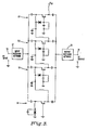
- Fig. 3 illustrates the manner in which an expanded amplifier circuit in accordance with the present invention can be constructed to provide N parallel ac amplifying paths with a single dc power supply path in series through N transistors.
- An RF input terminal 30 is connected through an appropriate input matching network 32 to several stages Sl-SN. The outputs of the stages are connected together and through an output matching network 33 to an RF output terminal 31.
- Each of the stages Sl... except the last stage SN in the plurality is similar to the stage employing the first transistor Ql in the circuit of Fig.l.
- the last stage SN in the plurality of stages is similar to the stage employing the second transistor Q2 in the circuit of Fig. 1.
- the dc current path is from the source of operating voltage V DD through each of the transistors of the stages Sl-SN in series to ground.
- the stage Sl-SN provide N parallel ac amplifying paths with the operating voltage V DD divided between them, thus providing for a very high amplifier operating potential.
Landscapes
- Engineering & Computer Science (AREA)
- Power Engineering (AREA)
- Amplifiers (AREA)
Applications Claiming Priority (2)
| Application Number | Priority Date | Filing Date | Title |
|---|---|---|---|
| US06/604,779 US4590437A (en) | 1984-04-27 | 1984-04-27 | High frequency amplifier |
| US604779 | 1996-02-23 |
Publications (3)
| Publication Number | Publication Date |
|---|---|
| EP0160223A2 true EP0160223A2 (de) | 1985-11-06 |
| EP0160223A3 EP0160223A3 (en) | 1987-11-25 |
| EP0160223B1 EP0160223B1 (de) | 1992-07-22 |
Family
ID=24421010
Family Applications (1)
| Application Number | Title | Priority Date | Filing Date |
|---|---|---|---|
| EP85103902A Expired EP0160223B1 (de) | 1984-04-27 | 1985-04-01 | Hochfrequenzverstärker |
Country Status (5)
| Country | Link |
|---|---|
| US (1) | US4590437A (de) |
| EP (1) | EP0160223B1 (de) |
| JP (1) | JPS60236306A (de) |
| CA (1) | CA1210093A (de) |
| DE (1) | DE3586368T2 (de) |
Cited By (1)
| Publication number | Priority date | Publication date | Assignee | Title |
|---|---|---|---|---|
| EP0442637B1 (de) * | 1990-02-16 | 1998-04-22 | Nokia Mobile Phones Ltd. | Schaltungsanordnung für die Verbindung von einem Hochfrequenzverstärker mit einem Versorgungsspannungsfilter |
Families Citing this family (14)
| Publication number | Priority date | Publication date | Assignee | Title |
|---|---|---|---|---|
| JPH0785528B2 (ja) * | 1989-12-25 | 1995-09-13 | 日本電気株式会社 | 高出力マイクロ波ミリ波トランジスタ安定化回路 |
| US5057791A (en) * | 1990-04-27 | 1991-10-15 | Harris Corporation | Device and method for bi-directional amplification with a JFET |
| DE69304522T2 (de) * | 1992-04-16 | 1997-01-23 | Advanced Energy Ind Inc | Stabilisator fuer schalt-mode geleistet radio-frequenz plasma einrichtung |
| WO1996031899A1 (en) | 1995-04-07 | 1996-10-10 | Advanced Energy Industries, Inc. | Adjustable energy quantum thin film plasma processing system |
| US5917286A (en) | 1996-05-08 | 1999-06-29 | Advanced Energy Industries, Inc. | Pulsed direct current power supply configurations for generating plasmas |
| JP4286911B2 (ja) | 1997-02-24 | 2009-07-01 | アドバンスト エナジー インダストリーズ,インコーポレイテッド | プラズマ処理方法及びプラズマ処理システム |
| US6791411B1 (en) | 1999-12-03 | 2004-09-14 | Infineon Technologies, Ag | Power amplifier and a method for operating a power amplifier |
| GB2376819A (en) * | 2001-06-21 | 2002-12-24 | Ericsson Telefon Ab L M | Electronic circuit having series connected circuit blocks |
| TWI377787B (en) * | 2007-01-04 | 2012-11-21 | Alpha Networks Inc | Input voltage-judging device and method for judging voltage range |
| JP2015019328A (ja) * | 2013-07-12 | 2015-01-29 | 住友電気工業株式会社 | 増幅回路 |
| JP6247188B2 (ja) | 2013-10-31 | 2017-12-13 | サムソン エレクトロ−メカニックス カンパニーリミテッド. | 積層セラミックキャパシタ |
| JP2020198570A (ja) * | 2019-06-04 | 2020-12-10 | 株式会社村田製作所 | 可変利得回路、高周波スイッチ、およびトランジスタ回路 |
| US12113486B2 (en) | 2020-11-20 | 2024-10-08 | The Boeing Company | Amplifier with stacked transconducting cells in parallel and/or cascade “current mode” combining |
| EP4120564A1 (de) * | 2021-07-16 | 2023-01-18 | The Boeing Company | Verstärker mit gestapelten transkonduktanzzellen in parallel- und/oder kaskadenstromkombination |
Family Cites Families (4)
| Publication number | Priority date | Publication date | Assignee | Title |
|---|---|---|---|---|
| CA652137A (en) * | 1959-02-11 | 1962-11-13 | Automatic Electric Laboratories | Transistor tone generator and power amplifier |
| FR1238817A (fr) * | 1959-07-07 | 1960-08-19 | Labo Cent Telecommunicat | Circuits amplificateurs à transistors |
| GB1054134A (de) * | 1964-02-28 | |||
| US4342967A (en) * | 1980-05-01 | 1982-08-03 | Gte Laboratories Incorporated | High voltage, high frequency amplifier |
-
1984
- 1984-04-27 US US06/604,779 patent/US4590437A/en not_active Expired - Lifetime
-
1985
- 1985-04-01 DE DE8585103902T patent/DE3586368T2/de not_active Expired - Fee Related
- 1985-04-01 EP EP85103902A patent/EP0160223B1/de not_active Expired
- 1985-04-15 CA CA000479180A patent/CA1210093A/en not_active Expired
- 1985-04-26 JP JP60089055A patent/JPS60236306A/ja active Pending
Cited By (1)
| Publication number | Priority date | Publication date | Assignee | Title |
|---|---|---|---|---|
| EP0442637B1 (de) * | 1990-02-16 | 1998-04-22 | Nokia Mobile Phones Ltd. | Schaltungsanordnung für die Verbindung von einem Hochfrequenzverstärker mit einem Versorgungsspannungsfilter |
Also Published As
| Publication number | Publication date |
|---|---|
| DE3586368D1 (de) | 1992-08-27 |
| US4590437A (en) | 1986-05-20 |
| EP0160223B1 (de) | 1992-07-22 |
| JPS60236306A (ja) | 1985-11-25 |
| CA1210093A (en) | 1986-08-19 |
| EP0160223A3 (en) | 1987-11-25 |
| DE3586368T2 (de) | 1993-01-07 |
Similar Documents
| Publication | Publication Date | Title |
|---|---|---|
| US4590436A (en) | High voltage, high frequency amplifier circuit | |
| US4342967A (en) | High voltage, high frequency amplifier | |
| US7068104B2 (en) | Power amplifier utilizing high breakdown voltage circuit topology | |
| EP0160223B1 (de) | Hochfrequenzverstärker | |
| US6778016B2 (en) | Simple self-biased cascode amplifier circuit | |
| US5920230A (en) | HEMT-HBT cascode distributed amplifier | |
| JPH08501425A (ja) | 高電力ソリッドステートrf増幅器 | |
| KR20010023834A (ko) | 접지되고 직렬접속되고 스택된 fet쌍을 가지는 토템 폴믹서 | |
| JP2004515937A (ja) | カスコード・ブートストラップ・アナログ電力増幅回路 | |
| US7560992B2 (en) | Dynamically biased amplifier | |
| KR20080016727A (ko) | 2단 마이크로웨이브 클래스 e 전력 증폭기 | |
| US6538515B2 (en) | Power amplifier and method of operating a power amplifier having multiple output-power modes | |
| US6498533B1 (en) | Bootstrapped dual-gate class E amplifier circuit | |
| US8022776B2 (en) | Origami cascaded topology for analog and mixed-signal applications | |
| US3835406A (en) | Neutralized amplifier circuit | |
| US20060006945A1 (en) | Parallel amplifier configuration with power combining and impedance transformation | |
| US4733194A (en) | Apparatus and method for paralleling power field effect transistors in high frequency amplifiers | |
| US6087900A (en) | Parallel push-pull amplifier using complementary device | |
| KR100882819B1 (ko) | 복수의 공통 게이트 트랜지스터를 이용한 캐스코드 구조의증폭기 | |
| JPWO2000067323A1 (ja) | 静電破壊保護回路を有する半導体集積回路 | |
| CN114362685B (zh) | 一种基于高q值差分耦合技术的功率放大器 | |
| US11251820B2 (en) | Circuit for processing radio frequency signal | |
| JPH07283659A (ja) | 高周波電流のおよび広帯域電流の増幅法 | |
| JPH0734526B2 (ja) | 発振装置 | |
| US10177741B1 (en) | Envelope tracking active circulator |
Legal Events
| Date | Code | Title | Description |
|---|---|---|---|
| PUAI | Public reference made under article 153(3) epc to a published international application that has entered the european phase |
Free format text: ORIGINAL CODE: 0009012 |
|
| AK | Designated contracting states |
Designated state(s): DE FR GB |
|
| PUAL | Search report despatched |
Free format text: ORIGINAL CODE: 0009013 |
|
| AK | Designated contracting states |
Kind code of ref document: A3 Designated state(s): DE FR GB |
|
| 17P | Request for examination filed |
Effective date: 19880520 |
|
| 17Q | First examination report despatched |
Effective date: 19900809 |
|
| GRAA | (expected) grant |
Free format text: ORIGINAL CODE: 0009210 |
|
| AK | Designated contracting states |
Kind code of ref document: B1 Designated state(s): DE FR GB |
|
| REF | Corresponds to: |
Ref document number: 3586368 Country of ref document: DE Date of ref document: 19920827 |
|
| ET | Fr: translation filed | ||
| PG25 | Lapsed in a contracting state [announced via postgrant information from national office to epo] |
Ref country code: GB Effective date: 19930401 |
|
| PLBE | No opposition filed within time limit |
Free format text: ORIGINAL CODE: 0009261 |
|
| STAA | Information on the status of an ep patent application or granted ep patent |
Free format text: STATUS: NO OPPOSITION FILED WITHIN TIME LIMIT |
|
| 26N | No opposition filed | ||
| GBPC | Gb: european patent ceased through non-payment of renewal fee |
Effective date: 19930401 |
|
| PG25 | Lapsed in a contracting state [announced via postgrant information from national office to epo] |
Ref country code: FR Effective date: 19931229 |
|
| PG25 | Lapsed in a contracting state [announced via postgrant information from national office to epo] |
Ref country code: DE Effective date: 19940101 |
|
| REG | Reference to a national code |
Ref country code: FR Ref legal event code: ST |