EP0160484A2 - FM-Empfänger der eine phasenverkoppelte Schleife für das Basisband enthält - Google Patents
FM-Empfänger der eine phasenverkoppelte Schleife für das Basisband enthält Download PDFInfo
- Publication number
- EP0160484A2 EP0160484A2 EP85302802A EP85302802A EP0160484A2 EP 0160484 A2 EP0160484 A2 EP 0160484A2 EP 85302802 A EP85302802 A EP 85302802A EP 85302802 A EP85302802 A EP 85302802A EP 0160484 A2 EP0160484 A2 EP 0160484A2
- Authority
- EP
- European Patent Office
- Prior art keywords
- signal
- complex
- frequency
- output
- low
- Prior art date
- Legal status (The legal status is an assumption and is not a legal conclusion. Google has not performed a legal analysis and makes no representation as to the accuracy of the status listed.)
- Withdrawn
Links
Images
Classifications
-
- H—ELECTRICITY
- H03—ELECTRONIC CIRCUITRY
- H03D—DEMODULATION OR TRANSFERENCE OF MODULATION FROM ONE CARRIER TO ANOTHER
- H03D3/00—Demodulation of angle-, frequency- or phase- modulated oscillations
- H03D3/02—Demodulation of angle-, frequency- or phase- modulated oscillations by detecting phase difference between two signals obtained from input signal
- H03D3/24—Modifications of demodulators to reject or remove amplitude variations by means of locked-in oscillator circuits
- H03D3/241—Modifications of demodulators to reject or remove amplitude variations by means of locked-in oscillator circuits the oscillator being part of a phase locked loop
- H03D3/245—Modifications of demodulators to reject or remove amplitude variations by means of locked-in oscillator circuits the oscillator being part of a phase locked loop using at least twophase detectors in the loop
-
- H—ELECTRICITY
- H03—ELECTRONIC CIRCUITRY
- H03L—AUTOMATIC CONTROL, STARTING, SYNCHRONISATION OR STABILISATION OF GENERATORS OF ELECTRONIC OSCILLATIONS OR PULSES
- H03L7/00—Automatic control of frequency or phase; Synchronisation
- H03L7/06—Automatic control of frequency or phase; Synchronisation using a reference signal applied to a frequency- or phase-locked loop
- H03L7/08—Details of the phase-locked loop
- H03L7/085—Details of the phase-locked loop concerning mainly the frequency- or phase-detection arrangement including the filtering or amplification of its output signal
- H03L7/087—Details of the phase-locked loop concerning mainly the frequency- or phase-detection arrangement including the filtering or amplification of its output signal using at least two phase detectors or a frequency and phase detector in the loop
-
- H—ELECTRICITY
- H03—ELECTRONIC CIRCUITRY
- H03B—GENERATION OF OSCILLATIONS, DIRECTLY OR BY FREQUENCY-CHANGING, BY CIRCUITS EMPLOYING ACTIVE ELEMENTS WHICH OPERATE IN A NON-SWITCHING MANNER; GENERATION OF NOISE BY SUCH CIRCUITS
- H03B27/00—Generation of oscillations providing a plurality of outputs of the same frequency but differing in phase, other than merely two anti-phase outputs
-
- H—ELECTRICITY
- H03—ELECTRONIC CIRCUITRY
- H03B—GENERATION OF OSCILLATIONS, DIRECTLY OR BY FREQUENCY-CHANGING, BY CIRCUITS EMPLOYING ACTIVE ELEMENTS WHICH OPERATE IN A NON-SWITCHING MANNER; GENERATION OF NOISE BY SUCH CIRCUITS
- H03B28/00—Generation of oscillations by methods not covered by groups H03B5/00 - H03B27/00, including modification of the waveform to produce sinusoidal oscillations
-
- H—ELECTRICITY
- H03—ELECTRONIC CIRCUITRY
- H03D—DEMODULATION OR TRANSFERENCE OF MODULATION FROM ONE CARRIER TO ANOTHER
- H03D2200/00—Indexing scheme relating to details of demodulation or transference of modulation from one carrier to another covered by H03D
- H03D2200/0001—Circuit elements of demodulators
- H03D2200/0031—PLL circuits with quadrature locking, e.g. a Costas loop
-
- H—ELECTRICITY
- H03—ELECTRONIC CIRCUITRY
- H03D—DEMODULATION OR TRANSFERENCE OF MODULATION FROM ONE CARRIER TO ANOTHER
- H03D7/00—Transference of modulation from one carrier to another, e.g. frequency-changing
- H03D7/16—Multiple-frequency-changing
- H03D7/165—Multiple-frequency-changing at least two frequency changers being located in different paths, e.g. in two paths with carriers in quadrature
-
- H—ELECTRICITY
- H03—ELECTRONIC CIRCUITRY
- H03D—DEMODULATION OR TRANSFERENCE OF MODULATION FROM ONE CARRIER TO ANOTHER
- H03D7/00—Transference of modulation from one carrier to another, e.g. frequency-changing
- H03D7/18—Modifications of frequency-changers for eliminating image frequencies
Definitions
- the present invention relates to generally an FM receiving circuit for use in a radio communication system and, more particularly, to an FM receiver including an improved baseband phase locked loop (PLL) circuit.
- PLL phase locked loop
- a conventional FM receiver is either of direct detection or of superheterodyne type.
- the direct detection type is defective in that it is difficult to obtain sufficient selectivity because the frequency selectivity is dependent on filters of the high-frequency bands. Since, in the superheterodyne type, a high-frequency input signal is converted into an intermediate frequency signal, and the frequency selectivity is determined by an intermediate frequency filter, better selectivity is achieved, compared with the direct detection type.
- the FM receiver tends to become sensitive to a frequency (an image frequency) which is apart from the frequency to be received by two times the intermediate frequency. In order to eliminate the component of the image frequency, a band-pass filter has to be provided between the high-frequency input terminal and the frequency conversion circuit.
- the use of the band-pass filter induces a loss of a receiving power. Moreover, when a receiving frequency is changed, the filter has to be changed, too. Such defects become more aggravating as the range of frequency to be received becomes wider. Providing a high-frequency filter or an intermediate-frequency filter has a problem in realizing higher integration of circuits.
- An object of the present invention is, therefore, to provide an FM receiver having a better selectivity, a wider range of frequency coverage, and higher integration.
- Another object of the invention is to provide an F M receiver directly converting an input signal to a baseband signal of about zero frequency by using a local oscillator signal of frequency substantially equal to the carrier frequency of the input signal.
- Further object of the invention is to provide an FM receiver in which only low-pass filters are used to obtain high frequency selectivity.
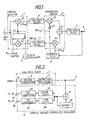
- an FM receiver for receiving an FM signal comprising: a complex detector for complex detecting the FM signal by using a local oscillator signal having a frequency substantially equal to the carrier frequency of the F M signal as a reference signal; a first low-pass filter for filtering the real part signal of the output complex signal from the complex detector; a second low-pass filter filtering the imaginary part signal of the complex signals; a complex voltage-controlled oscillator operating both in the positive and the negative frequency ranges including the zero frequency and being frequency-controllable with a frequency control signal; an operational circuit for taking out one of an imaginary part and a real part signals of a product of an output complex conjugate signal from the complex voltage-controlled oscillator and the filtered complex signals from the first and second low-pass filters; and a third low-pass filter for filtering the output of the operational circuit to provide a demodulated output and to feed it back as the frequency control signal to the complex voltage-controlled oscillator.
- the reference number 1 denotes an input terminal and 2 a complex detector which comprises product detectors 21 and 22 and a ⁇ /2 phase shifter 23.
- the reference number 3 denotes a local oscillator which generates a signal of frequency substantially equal to the carrier frequency of an input signal to be applied to the terminal 1, 4 a first low-pass filter (LPF), 5 a second LPF and 6 an operational circuit which comprises multipliers 61 and 62, an inverter 63 and an adder 64.
- the reference number 7 denotes a third LPF, 8 acomplex voltage-controlled oscillator (VCO), and 9 an output terminal.
- LPF low-pass filter
- VCO voltage-controlled oscillator
- ⁇ 1 and ⁇ 2 denote each angular frequency (or angular velocity) and t time. Coefficients are omitted in both (the same applies hereinafter).
- the angular velocity ⁇ 2 of the output signal from the local oscillator 3 is preferably made coincide with but not necessarily synchronized with the angular velocity ⁇ 1 of the input signal.
- the low frequency component sin ⁇ 3 t of the product of cos ⁇ 1 t and cos ( ⁇ 2 t + ⁇ /2) is obtained.
- the complex detection output cos ⁇ 3 t + jsin ⁇ 3 t is obtained (wherein j denotes a unit of imaginary number).
- the complex detection output is restricted in band as it passes through the first LPF 4 and the second LPF 5.
- the filters operate to allow the signals pass only when f 3 ⁇ B, or when
- the LPFs 4 and 5 have the frequency selectivity which is sensitive only when f l is within the range of ⁇ B from f 2 .
- the low-pass filters may have precipitious cutoff characteristics and, therefore, a very steep selectivity can be obtained irrespective of the center frequency f 2 .
- the complex detection output signals which have passed through the LPFs 4 and 5 will be processed with the output signal of the complex VCO 8 in the operational circuit 6.
- the process of the operational circuit 6 will be conducted in such a way to take out the imaginary part of the complex multiplication between the complex conjugate number of the output of the oscillator 8 and complex detection output signal.
- the inverter 63 inverts the polarity of sin ⁇ 4 t in order to form a complex conjugation.
- the multiplier 61 multiplies cos ⁇ 3 t with -sin ⁇ 4 t, and the multiplier 62 multiplies sin ⁇ 3 t with cos ⁇ 4 t.
- the PLL circuit of the present invention differs from the conventional one in that it is intended to synchronize the complex signals, to have the merit that it is capable of operating even when ⁇ 3 and ⁇ 4 are in the negative range.
- the input signal is frequency-modulated (e.i., FM signal)
- ⁇ 1 changes in proportion to the modulation signal
- ⁇ 4 changes in proportion to the modulation signal.
- the signal can be taken out from the output terminal 9 as a demodulated signal.
- the FM signal may include an frequency shift keyed (FSK) signal.
- an FM receiver having excellent selection characteristics can be obtained by the present invention without using band-pass filters. It is also evident from the foregoing that the FM receiver according to the present invention is capable of covering a wider range of frequencies by merely changing the frequency of the local oscillator 3.
- the reference number 10 denotes an input terminal for signals from the operational circuit 6 (Fig. 1), 11 a comparator for judging the polarity of the input applied thereto, and 71 a digital low-pass filter which is operable when supplied with a binary signal.
- the complex VCO 8 comprises an adder 81, a memory 82, a read-only memory (ROM) 83 which stbres cosine waveforms, a ROM 84 which stores sine waveforms, digital/analog converters 85 and 86, a real part output terminal 87, and an imaginary part output terminal 88.
- the comparator 11 functions as a limiter to absorb the level change in the input signals.
- the adder 81 and the memory 82 function as integrators, and when a positive input is received, the output increases and when a negative input is received, the output decreases. It should be noted that the memory 82 and the adder 81 have a limited number of digits and perform modulo operation to return to zero when overflow occurs. The value at which overflow occurs is made to correspond to 360° of the phase.
- the output of the integrator is fed to the ROMs 83 and 84 as an address input.
- the ROMs 83 and 84 use the address input as an phase input, and supply the output values of cosine and sine corresponding thereto to digital/ analog converters 85 and 86, respectively. Then, the output values are converted into analog waveforms by the digital/analog converters 85 and 86 and outputted from the output terminals 87 and 88.
- the greater and positive the value of the control signal to be fed to the adder 81 is, the greater the curve of increase in the value of the integrator becomes, whereby the waveforms at the output terminals 87 and 88 show a rapid change and a signal having a higher frequency can be obtained.
- the output of the integrator stops changing and DC outputs can be obtained at the output terminals 87 and 88. In other words, signals of zero frequency can be obtained.
- the control signal becomes negative, the output of the integrator decreases and whereby a cosine wave and a sine wave are obtained at the terminals 87 and 88, respectively. Contrary to the case where the frequency is positive, the phase relationship between the cosine and sine waves is inverted. In other words, negative frequency signals are obtained.
- the embodiment has been described in the above with respect to the complex VCO. It is noted, however, that the ROM 84 storing the since waveforms can be switched for use as the ROM 83 storing the cosine waveforms by reducing the address by the angle of 90°. It is also a common practice to save the ROM capacity by making the ROM store the values in the range of from 0° to 90° instead of all the values covering the range of from 0° to 360° and obtain desired outputs by means of address conversion and the output conversion.
- an LPF having an excellent frequency selectivity can be used as a frequency selection means for the input signals received.
- the FM receiver of the present invention does not require a high frequency band-pass filter, there is no restriction as to the frequency range caused by such high frequency band-pass filter and the frequency can be easily changed over a wider frequency range by merely changing the frequency of the local oscillator.
Landscapes
- Engineering & Computer Science (AREA)
- Power Engineering (AREA)
- Superheterodyne Receivers (AREA)
- Digital Transmission Methods That Use Modulated Carrier Waves (AREA)
- Stabilization Of Oscillater, Synchronisation, Frequency Synthesizers (AREA)
Applications Claiming Priority (2)
| Application Number | Priority Date | Filing Date | Title |
|---|---|---|---|
| JP8160284A JPS60224337A (ja) | 1984-04-23 | 1984-04-23 | 受信回路 |
| JP81602/84 | 1984-04-23 |
Publications (2)
| Publication Number | Publication Date |
|---|---|
| EP0160484A2 true EP0160484A2 (de) | 1985-11-06 |
| EP0160484A3 EP0160484A3 (de) | 1987-04-29 |
Family
ID=13750862
Family Applications (1)
| Application Number | Title | Priority Date | Filing Date |
|---|---|---|---|
| EP85302802A Withdrawn EP0160484A3 (de) | 1984-04-23 | 1985-04-22 | FM-Empfänger der eine phasenverkoppelte Schleife für das Basisband enthält |
Country Status (3)
| Country | Link |
|---|---|
| EP (1) | EP0160484A3 (de) |
| JP (1) | JPS60224337A (de) |
| AU (1) | AU4163285A (de) |
Cited By (2)
| Publication number | Priority date | Publication date | Assignee | Title |
|---|---|---|---|---|
| EP0754368A4 (de) * | 1994-04-05 | 1997-07-23 | Scientific Atlanta | Synchrondetektor und verfahren zur synchronen detektion |
| WO2005107056A1 (en) * | 2004-05-04 | 2005-11-10 | Telefonaktiebolaget Lm Ericsson (Publ) | Xo-buffer robust to interference |
Family Cites Families (4)
| Publication number | Priority date | Publication date | Assignee | Title |
|---|---|---|---|---|
| US3600700A (en) * | 1968-06-12 | 1971-08-17 | Nippon Electric Co | Circuit for phase locking an oscillator to a signal modulated in n-phases |
| US4234957A (en) * | 1978-12-04 | 1980-11-18 | Gte Automatic Electric Laboratories Incorporated | Method and apparatus for generating timing phase error signals in PSK demodulators |
| DE2902952C2 (de) * | 1979-01-26 | 1986-10-09 | ANT Nachrichtentechnik GmbH, 7150 Backnang | Direktmischendes Empfangssystem |
| GB2052196A (en) * | 1979-06-27 | 1981-01-21 | Plessey Co Ltd | Demodulators |
-
1984
- 1984-04-23 JP JP8160284A patent/JPS60224337A/ja active Granted
-
1985
- 1985-04-22 EP EP85302802A patent/EP0160484A3/de not_active Withdrawn
- 1985-04-23 AU AU41632/85A patent/AU4163285A/en not_active Abandoned
Cited By (3)
| Publication number | Priority date | Publication date | Assignee | Title |
|---|---|---|---|---|
| EP0754368A4 (de) * | 1994-04-05 | 1997-07-23 | Scientific Atlanta | Synchrondetektor und verfahren zur synchronen detektion |
| WO2005107056A1 (en) * | 2004-05-04 | 2005-11-10 | Telefonaktiebolaget Lm Ericsson (Publ) | Xo-buffer robust to interference |
| US7102447B2 (en) | 2004-05-04 | 2006-09-05 | Telefonaktiebolaget L M Ericsson (Publ) | XO-buffer robust to interference |
Also Published As
| Publication number | Publication date |
|---|---|
| JPH0332933B2 (de) | 1991-05-15 |
| JPS60224337A (ja) | 1985-11-08 |
| EP0160484A3 (de) | 1987-04-29 |
| AU4163285A (en) | 1985-10-31 |
Similar Documents
| Publication | Publication Date | Title |
|---|---|---|
| EP0305603B1 (de) | Phasen- und Verstärkungsregelung für einen Empfänger mit zwei Zweigen | |
| JP3647894B2 (ja) | アナログオーバーサンプリングを用いて信号帯域幅を増大する中間周波数fm受信機 | |
| US4476585A (en) | Baseband demodulator for FM signals | |
| US3961262A (en) | FM receiver and demodulation circuit | |
| US6195400B1 (en) | Two-mode demodulating apparatus | |
| US4672636A (en) | AFC circuit for direct modulation FM data receivers | |
| CA1151735A (en) | Broadcast signal receiving system for directly recovering the modulating signal from a received modulated high frequency signal | |
| GB2170368A (en) | Receiver for mobile communication systems | |
| JPH03235078A (ja) | Gps受信機の衛星電波捕捉方法 | |
| KR19980015790A (ko) | 직각 위상 편이 복조기의 자동 이득 제어장치 | |
| US5703527A (en) | Frequency modulated signal demodulator circuit and communication terminal equipment | |
| US4599743A (en) | Baseband demodulator for FM and/or AM signals | |
| US4677690A (en) | Baseband demodulator for FM and/or AM signals | |
| JPH01135223A (ja) | 周波数差検出器 | |
| US4493099A (en) | FM Broadcasting system with transmitter identification | |
| US3873931A (en) | FM demodulator circuits | |
| EP0160484A2 (de) | FM-Empfänger der eine phasenverkoppelte Schleife für das Basisband enthält | |
| US2930891A (en) | Receiving system for suppressed or reduced carrier waves with phase-locked synchronous detector | |
| JPH07202574A (ja) | 復調器 | |
| US5648823A (en) | Circuit configuration for intermediate frequency demodulation and device for video signal processing including the circuit | |
| US4578706A (en) | Television synchronous receiver | |
| JPH09200072A (ja) | 直接変換受信機 | |
| JP3335414B2 (ja) | 周波数変換による被振幅変調隣接妨害除去装置 | |
| JP3335411B2 (ja) | 周波数変換による被振幅変調隣接妨害検出装置 | |
| JPS59196629A (ja) | Fm受信機 |
Legal Events
| Date | Code | Title | Description |
|---|---|---|---|
| PUAI | Public reference made under article 153(3) epc to a published international application that has entered the european phase |
Free format text: ORIGINAL CODE: 0009012 |
|
| 17P | Request for examination filed |
Effective date: 19850510 |
|
| AK | Designated contracting states |
Designated state(s): DE FR GB NL |
|
| PUAL | Search report despatched |
Free format text: ORIGINAL CODE: 0009013 |
|
| AK | Designated contracting states |
Kind code of ref document: A3 Designated state(s): DE FR GB NL |
|
| 17Q | First examination report despatched |
Effective date: 19871123 |
|
| STAA | Information on the status of an ep patent application or granted ep patent |
Free format text: STATUS: THE APPLICATION IS DEEMED TO BE WITHDRAWN |
|
| 18D | Application deemed to be withdrawn |
Effective date: 19880406 |
|
| RIN1 | Information on inventor provided before grant (corrected) |
Inventor name: MATSUO, YOSHIO |