EP0160490A2 - Halbleiterlaser - Google Patents
Halbleiterlaser Download PDFInfo
- Publication number
- EP0160490A2 EP0160490A2 EP85302819A EP85302819A EP0160490A2 EP 0160490 A2 EP0160490 A2 EP 0160490A2 EP 85302819 A EP85302819 A EP 85302819A EP 85302819 A EP85302819 A EP 85302819A EP 0160490 A2 EP0160490 A2 EP 0160490A2
- Authority
- EP
- European Patent Office
- Prior art keywords
- layer
- channel
- substrate
- semiconductor laser
- cladding layer
- Prior art date
- Legal status (The legal status is an assumption and is not a legal conclusion. Google has not performed a legal analysis and makes no representation as to the accuracy of the status listed.)
- Granted
Links
- 239000004065 semiconductor Substances 0.000 title claims abstract description 40
- 238000005253 cladding Methods 0.000 claims abstract description 43
- 239000000758 substrate Substances 0.000 claims abstract description 40
- 230000010355 oscillation Effects 0.000 claims abstract description 27
- 239000013078 crystal Substances 0.000 claims abstract description 19
- 239000000945 filler Substances 0.000 claims description 10
- 238000004943 liquid phase epitaxy Methods 0.000 claims description 9
- 229910001218 Gallium arsenide Inorganic materials 0.000 description 14
- 238000000034 method Methods 0.000 description 13
- 230000000903 blocking effect Effects 0.000 description 6
- 239000012535 impurity Substances 0.000 description 6
- 230000004888 barrier function Effects 0.000 description 5
- 230000015572 biosynthetic process Effects 0.000 description 3
- 239000000969 carrier Substances 0.000 description 3
- 238000011109 contamination Methods 0.000 description 3
- 238000009792 diffusion process Methods 0.000 description 3
- 230000007423 decrease Effects 0.000 description 2
- 230000000694 effects Effects 0.000 description 2
- 238000005530 etching Methods 0.000 description 2
- 238000002360 preparation method Methods 0.000 description 2
- OKTJSMMVPCPJKN-UHFFFAOYSA-N Carbon Chemical compound [C] OKTJSMMVPCPJKN-UHFFFAOYSA-N 0.000 description 1
- 238000002109 crystal growth method Methods 0.000 description 1
- 230000003247 decreasing effect Effects 0.000 description 1
- 230000007812 deficiency Effects 0.000 description 1
- 229910002804 graphite Inorganic materials 0.000 description 1
- 239000010439 graphite Substances 0.000 description 1
- 239000007791 liquid phase Substances 0.000 description 1
- 238000004519 manufacturing process Methods 0.000 description 1
- 239000000463 material Substances 0.000 description 1
- 239000002184 metal Substances 0.000 description 1
- 238000001451 molecular beam epitaxy Methods 0.000 description 1
- 238000000927 vapour-phase epitaxy Methods 0.000 description 1
- 230000010356 wave oscillation Effects 0.000 description 1
Images

Classifications
-
- H—ELECTRICITY
- H01—ELECTRIC ELEMENTS
- H01S—DEVICES USING THE PROCESS OF LIGHT AMPLIFICATION BY STIMULATED EMISSION OF RADIATION [LASER] TO AMPLIFY OR GENERATE LIGHT; DEVICES USING STIMULATED EMISSION OF ELECTROMAGNETIC RADIATION IN WAVE RANGES OTHER THAN OPTICAL
- H01S5/00—Semiconductor lasers
- H01S5/20—Structure or shape of the semiconductor body to guide the optical wave ; Confining structures perpendicular to the optical axis, e.g. index or gain guiding, stripe geometry, broad area lasers, gain tailoring, transverse or lateral reflectors, special cladding structures, MQW barrier reflection layers
- H01S5/24—Structure or shape of the semiconductor body to guide the optical wave ; Confining structures perpendicular to the optical axis, e.g. index or gain guiding, stripe geometry, broad area lasers, gain tailoring, transverse or lateral reflectors, special cladding structures, MQW barrier reflection layers having a grooved structure, e.g. V-grooved, crescent active layer in groove, VSIS laser
-
- H—ELECTRICITY
- H01—ELECTRIC ELEMENTS
- H01S—DEVICES USING THE PROCESS OF LIGHT AMPLIFICATION BY STIMULATED EMISSION OF RADIATION [LASER] TO AMPLIFY OR GENERATE LIGHT; DEVICES USING STIMULATED EMISSION OF ELECTROMAGNETIC RADIATION IN WAVE RANGES OTHER THAN OPTICAL
- H01S5/00—Semiconductor lasers
- H01S5/30—Structure or shape of the active region; Materials used for the active region
- H01S5/32—Structure or shape of the active region; Materials used for the active region comprising PN junctions, e.g. hetero- or double- heterostructures
- H01S5/323—Structure or shape of the active region; Materials used for the active region comprising PN junctions, e.g. hetero- or double- heterostructures in AIIIBV compounds, e.g. AlGaAs-laser, InP-based laser
-
- H—ELECTRICITY
- H01—ELECTRIC ELEMENTS
- H01S—DEVICES USING THE PROCESS OF LIGHT AMPLIFICATION BY STIMULATED EMISSION OF RADIATION [LASER] TO AMPLIFY OR GENERATE LIGHT; DEVICES USING STIMULATED EMISSION OF ELECTROMAGNETIC RADIATION IN WAVE RANGES OTHER THAN OPTICAL
- H01S5/00—Semiconductor lasers
- H01S5/20—Structure or shape of the semiconductor body to guide the optical wave ; Confining structures perpendicular to the optical axis, e.g. index or gain guiding, stripe geometry, broad area lasers, gain tailoring, transverse or lateral reflectors, special cladding structures, MQW barrier reflection layers
- H01S5/22—Structure or shape of the semiconductor body to guide the optical wave ; Confining structures perpendicular to the optical axis, e.g. index or gain guiding, stripe geometry, broad area lasers, gain tailoring, transverse or lateral reflectors, special cladding structures, MQW barrier reflection layers having a ridge or stripe structure
- H01S5/223—Buried stripe structure
- H01S5/2232—Buried stripe structure with inner confining structure between the active layer and the lower electrode
- H01S5/2234—Buried stripe structure with inner confining structure between the active layer and the lower electrode having a structured substrate surface
-
- H—ELECTRICITY
- H01—ELECTRIC ELEMENTS
- H01S—DEVICES USING THE PROCESS OF LIGHT AMPLIFICATION BY STIMULATED EMISSION OF RADIATION [LASER] TO AMPLIFY OR GENERATE LIGHT; DEVICES USING STIMULATED EMISSION OF ELECTROMAGNETIC RADIATION IN WAVE RANGES OTHER THAN OPTICAL
- H01S5/00—Semiconductor lasers
- H01S5/20—Structure or shape of the semiconductor body to guide the optical wave ; Confining structures perpendicular to the optical axis, e.g. index or gain guiding, stripe geometry, broad area lasers, gain tailoring, transverse or lateral reflectors, special cladding structures, MQW barrier reflection layers
- H01S5/22—Structure or shape of the semiconductor body to guide the optical wave ; Confining structures perpendicular to the optical axis, e.g. index or gain guiding, stripe geometry, broad area lasers, gain tailoring, transverse or lateral reflectors, special cladding structures, MQW barrier reflection layers having a ridge or stripe structure
- H01S5/223—Buried stripe structure
- H01S5/2237—Buried stripe structure with a non-planar active layer
-
- H—ELECTRICITY
- H01—ELECTRIC ELEMENTS
- H01S—DEVICES USING THE PROCESS OF LIGHT AMPLIFICATION BY STIMULATED EMISSION OF RADIATION [LASER] TO AMPLIFY OR GENERATE LIGHT; DEVICES USING STIMULATED EMISSION OF ELECTROMAGNETIC RADIATION IN WAVE RANGES OTHER THAN OPTICAL
- H01S5/00—Semiconductor lasers
- H01S5/30—Structure or shape of the active region; Materials used for the active region
- H01S5/305—Structure or shape of the active region; Materials used for the active region characterised by the doping materials used in the laser structure
- H01S5/3054—Structure or shape of the active region; Materials used for the active region characterised by the doping materials used in the laser structure p-doping
-
- H—ELECTRICITY
- H01—ELECTRIC ELEMENTS
- H01S—DEVICES USING THE PROCESS OF LIGHT AMPLIFICATION BY STIMULATED EMISSION OF RADIATION [LASER] TO AMPLIFY OR GENERATE LIGHT; DEVICES USING STIMULATED EMISSION OF ELECTROMAGNETIC RADIATION IN WAVE RANGES OTHER THAN OPTICAL
- H01S5/00—Semiconductor lasers
- H01S5/30—Structure or shape of the active region; Materials used for the active region
- H01S5/32—Structure or shape of the active region; Materials used for the active region comprising PN junctions, e.g. hetero- or double- heterostructures
- H01S5/3211—Structure or shape of the active region; Materials used for the active region comprising PN junctions, e.g. hetero- or double- heterostructures characterised by special cladding layers, e.g. details on band-discontinuities
-
- H—ELECTRICITY
- H01—ELECTRIC ELEMENTS
- H01S—DEVICES USING THE PROCESS OF LIGHT AMPLIFICATION BY STIMULATED EMISSION OF RADIATION [LASER] TO AMPLIFY OR GENERATE LIGHT; DEVICES USING STIMULATED EMISSION OF ELECTROMAGNETIC RADIATION IN WAVE RANGES OTHER THAN OPTICAL
- H01S5/00—Semiconductor lasers
- H01S5/30—Structure or shape of the active region; Materials used for the active region
- H01S5/32—Structure or shape of the active region; Materials used for the active region comprising PN junctions, e.g. hetero- or double- heterostructures
- H01S5/323—Structure or shape of the active region; Materials used for the active region comprising PN junctions, e.g. hetero- or double- heterostructures in AIIIBV compounds, e.g. AlGaAs-laser, InP-based laser
- H01S5/32308—Structure or shape of the active region; Materials used for the active region comprising PN junctions, e.g. hetero- or double- heterostructures in AIIIBV compounds, e.g. AlGaAs-laser, InP-based laser emitting light at a wavelength less than 900 nm
Definitions
- This invention relates to a semiconductor laser having a doubleheterostructure on a striped channel substrate.
- Semiconductor lasers for laser oscillation at a long wavelength of visible light are known.
- a crystalline layer is grown on a V- or U-shaped channel substrate by an epitaxial growth technique, wherein the channel in the substrate must not be deformed during the epitaxial growth of the layer.
- MBE molecular beam epitaxy
- MO-VPE metal organic-vapor phase epitaxy
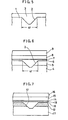
- a crystalline layer 3 is grown using liquid phase epitaxy (LPE) as the epitaxial growth technique to completely fill the channel 2, creating the formation shown in Figure 2, resulting in a growth layer having a plane surface.
- LPE liquid phase epitaxy
- Semiconductor lasers for laser oscillation at a short wave length of visible light are also known.
- the first cladding layer is used to fill the channel in the substrate, resulting in the following drawbacks:
- FIG. 3 of the accompanying drawings shows a VSIS (V-shaped channel substrate inner stripe) semiconductor laser with a plane active layer, which was disclosed in TGED 81-42, 31 (1981-July) IECE Japan, comprising a p-GaAs substrate 11, an n-GaAs current blocking layer 12, a p-Ga 1-y AlyAs cladding layer 13, a p-Ga l - x Al x As active layer 14, an n-Ga l- yAlyAs cladding layer 15 and an n-GaAs cap layer 16.
- the V-shaped channel 17 serves as an electroconductive region.
- the mole ratio y of AlAs to GaAs in the cladding layers 13 and 15 must be 0.6 or more.
- the mole ratio is less than 0.6, carriers leak out of the active layer 14 to the cladding layers 13 and 15 resulting in an increase in the threshold current and a decrease in the dependency of the threshold current upon temperature.
- extensive leakage of carriers (i.e., electrons) from the active layer 14 to the p-cladding layer 13 tends to take place, so that a considerably high barrier must be set to prevent such leakage of electrons to the p-cladding layer 13..
- the height of the barrier depends not only upon the mole-ratio y of AlAs to GaAs but also the positive hole concentration of the p-cladding layer 13. For example, when the positive hole concentration is 5 x 10 17 cm -3 , the barrier must be raised to approximately 50 meV (i.e., a 20 percent raise of the original barrier). This means that the positive hole concentration of the p-cladding layer 13 must be at least 1 x 10 18 cm- 3 .
- Mg is pref-erably used as a p-impurity since the addition of Mg in a concentration of 0.3 atomic percent or more to the p-cladding layer attains a carrier (positive hole) concentration of 1 x 10 18 cm -3 or more.
- Mg is doped to the Ga l -yAlyAs to a great extent, the growth rate of the crystalline layer decreases because Mg functions to reduce the diffusion coefficient of As in the Ga solution.
- the portion of the p-cladding layer 13 on the outside of the channel 17 becomes too thick to serve as a waveguide.
- the addition of Mg ir. the selected concentration to the p-cladding Ga 1-y Al y As (y>0.6) layer in a conventional manner to obtain a positive hole concentration of at least 1 x 10 18 cm -3 in the p-cladding layer cannot attain a good yield of semiconductor lasers having excellent characteristics and good reproducibility of the characteristics of the lasers.
- the semiconductor laser of this invention which is intended to overcome the above-discussed disadvantages and numerous other drawbacks and deficiencies of the prior art, comprises a substrate for crystal growth having a striped channel, an active layer for laser oscillation, and a cladding layer containing Mg which is in contact with the side of said active layer at least in the region which faces said striped channel.
- the cladding layer can be formed on the striped channel substrate by liquid phase epitaxy using a crystal growth solution containing Mg in a concentration of 0.3 atomic percent or more.
- a filler layer can be disposed between the striped channel substrate and the cladding layer to fill the channel in said substrate, the Mg content of said filler layer being less than that of said claddina layer.
- the invention described here in makes possible the objects of (1) providing a novel and useful semiconductor lafer for lasser oscillation at a long wavelength of visible light, wherein. the channel in the substrate is not deformed (i.e., the channel does not undergo meltback) during the epitaxial growth of the crystalline layer to fill the channel; and (2) providing a novel and useful semiconductor laser for laser oscillation at a short wavelength of visible light which has a cladding layer containing a sufficient carrier concentration thereby attaining an excellent yield and an excellent reproducibility of characteristics.
- Tne semiconductor laser for laser oscillation at a long wavelength of visible light of this invention can be constructed based on the experimental results that deformation of the channel in the substrate is minimal and the original with W thereof as shown in Figure 5 is maintained when a crystalline layer is formed on the substrate by an epitaxial growth technique using a crystal growth solution containing Mg of 0.3 atomic percent concentration or more. Mg attains the reduction of the diffusion coefficient of the solute in the crystal growth solution, thereby decreasing the initial growth rate of the. crystalline layer in the bottom of the channel.
- the vicinity of the shoulder of the channel is not short of solute, and accordingly the substrate does not undergo meltback, so that the width W of the channel is maintained and contamination by impurities from the substrate 1 to the gorwth layer 3 can be prevented, resulting in a device having excellent characteristics.
- Mg is a when the growth layer 3 is of a p-type (positive conducting type), while Mg is added together with n-impurities such as Te, etc., when the growth layer 3 is used as an n-type (negative conducting type).
- the semiconductor laser for laser oscillation at a short wavelength of visible light of this invention can be produced as followed:
- a semiconductor device having high quality crystal layers such as a semiconductor laser for laser oscillation at a long wavelength of visible light is produced, for example, using a liquid phase epitaxial growth technique of a sliding type, wherein a graphite boat including a crystal growth solution therein is moved on a substrate holder to coat a substrate fixed to the holder with the crystal growth solution to form a growth layer.
- a liquid phase epitaxial growth technique of a sliding type wherein a graphite boat including a crystal growth solution therein is moved on a substrate holder to coat a substrate fixed to the holder with the crystal growth solution to form a growth layer.
- Figure 6 shows a semiconductor laser for laser oscillation at a long wavelength of this invention using the above-mentioned technique, which was produced as follows:
- a p-cladding layer containing Mg in a concentration of 0.1 atomic percent was formed in the same manner as the above-mentioned.
- the width of the channel in the resulting semiconductor laser was greater than the original as shown in Figure 2.
- the reference standard laser oscillated at a wavelength of 780 nm and exhibited a far-field pattern which is at an angle ranging from 9.5° to 10.5° from the active layer.
- the width of the channel in the semiconductor laser of this invention obtained by the above-mentioned process was maintained at the original width W as shown in Figure 6.
- Each of the semiconductor laser units according to this invention exhibited uniform characteristics, especially uniform threshold current and a uniform lateral far-field pattern which is parallel to the junction, although a conventional semiconductor laser exhibited a non-uniform threshold current and a non-uniform lateral far-field patterr. parallel to the junction. Moreovr, in the semiconductor laser of this invention, contamination by impurities from the n-GaAs current blocking layer 5 to the p-cladding layer 6 is prevented resulting in improved reliability of the laser.
- the p-cladding layer 6 is grown using a Mg-doped GaAlAs solution (containing Mg of 0.3 atomic percent concentration or more) under the control of the initial growth rate by Mg in the bottom of the channel 2, the solute concentration in the GaAlAs solution is always maintained at a certain level during the epitaxial growth thereby preventing meltback in the shoulder portions of the channel 2 and contamination by components from the substrate 4 to the p-cladding layer 6.
- the Mg component which was doped to the p-cladding layer 6 is used as a p-impurity and the doping amount of Mg is selected to be 0.3 atomic percent concentration or more depending upon the desired carrier concentration.
- the crystal growth method in Example 1 is not limited to the GaAs-GaAlAs system, but it can be applied to liquid phase epitaxy for other semiconductor devices of an InP-InGaAsP system etc.
- Figure 7 shows a VSIS semiconductor laser for laser oscillation at a short wavelength of 700 mm or less of visible light, which was produced using a liquid phase epitaxy technique of a sliding type as follows :
- the VSIS semiconductor laser in this example attained laser oscillation at a wavelength in the range from 680 to 700 nm at a threshold current of as small as 70 mA on the average.
- the dependency of the laser of the threshold current upon the temperature was as small as 0.6 mA/°C.
- Most of the semiconductor laser units in a wafer attained laser oscillation at a threshold current of 100 mA or less and were superior in the reproducibility of laser oscillation. It is known that some of the conventional semiconductor lasers attain continuous wave oscillation at a wavelength of 683 nm which is the shortest oscillation wavelength of known semiconductor lasers (Appl. Phys-Lett. vol. 41, p.796, 1982).
- the composition ratio of the mixed crystal is 0.6 or more which is extremely great, the positive hole concentration is as hiah as around 1 x 10 18 cm -3 so that the threshold current level is reduced anc reproducibility of the device characteristics can be improved.
- the VSIS semiconductor laser of this invention is not limited to the GaAs-GaAlAs system, but it can be applied to a material such as, for example, an InP-InGaAsP system or a GaAsSb-AlGaAsSb system.
Landscapes
- Physics & Mathematics (AREA)
- Condensed Matter Physics & Semiconductors (AREA)
- General Physics & Mathematics (AREA)
- Electromagnetism (AREA)
- Optics & Photonics (AREA)
- Geometry (AREA)
- Semiconductor Lasers (AREA)
- Liquid Deposition Of Substances Of Which Semiconductor Devices Are Composed (AREA)
Applications Claiming Priority (4)
| Application Number | Priority Date | Filing Date | Title |
|---|---|---|---|
| JP83251/84 | 1984-04-24 | ||
| JP8325184A JPS60225490A (ja) | 1984-04-24 | 1984-04-24 | 半導体レーザ素子の製造方法 |
| JP83250/84 | 1984-04-24 | ||
| JP8325084A JPS60225423A (ja) | 1984-04-24 | 1984-04-24 | 液相エピタキシヤル成長方法 |
Related Child Applications (1)
| Application Number | Title | Priority Date | Filing Date |
|---|---|---|---|
| EP90118783.1 Division-Into | 1990-10-01 |
Publications (3)
| Publication Number | Publication Date |
|---|---|
| EP0160490A2 true EP0160490A2 (de) | 1985-11-06 |
| EP0160490A3 EP0160490A3 (en) | 1987-07-15 |
| EP0160490B1 EP0160490B1 (de) | 1992-07-08 |
Family
ID=26424303
Family Applications (2)
| Application Number | Title | Priority Date | Filing Date |
|---|---|---|---|
| EP85302819A Expired EP0160490B1 (de) | 1984-04-24 | 1985-04-23 | Halbleiterlaser |
| EP90118783A Expired - Lifetime EP0412582B1 (de) | 1984-04-24 | 1985-04-23 | Halbleiterlaser |
Family Applications After (1)
| Application Number | Title | Priority Date | Filing Date |
|---|---|---|---|
| EP90118783A Expired - Lifetime EP0412582B1 (de) | 1984-04-24 | 1985-04-23 | Halbleiterlaser |
Country Status (3)
| Country | Link |
|---|---|
| US (1) | US4792960A (de) |
| EP (2) | EP0160490B1 (de) |
| DE (2) | DE3587702T2 (de) |
Cited By (2)
| Publication number | Priority date | Publication date | Assignee | Title |
|---|---|---|---|---|
| EP0693810A3 (de) * | 1994-07-18 | 1996-04-03 | Sharp Kk | Halbleiterlaservorrichtung mit Begrenzungs- und Kontaktschichten dotiert mit Mg und Herstellungsverfahren |
| US6009113A (en) * | 1994-07-18 | 1999-12-28 | Sharp Kabushiki Kaisha | Semiconductor laser device having clad and contact layers respectively doped with Mg and method for fabricating the same |
Families Citing this family (6)
| Publication number | Priority date | Publication date | Assignee | Title |
|---|---|---|---|---|
| JPH03127891A (ja) * | 1989-10-13 | 1991-05-30 | Mitsubishi Electric Corp | 半導体レーザ装置 |
| JPH0461292A (ja) * | 1990-06-28 | 1992-02-27 | Mitsubishi Electric Corp | 半導体レーザ |
| DE4035994A1 (de) * | 1990-11-12 | 1992-05-14 | Siemens Ag | Schaltung und verfahren zur anpassung von antennen in einem kernspinresonanz-bildgeraet |
| JPH1012958A (ja) * | 1996-06-19 | 1998-01-16 | Mitsubishi Electric Corp | 半導体レーザ装置,及びその製造方法 |
| US20030063645A1 (en) * | 2001-09-28 | 2003-04-03 | The Furukawa Electric Co., Ltd. | Semiconductor laser device and method for suppressing fabry perot oscillations |
| US11217964B2 (en) * | 2018-12-28 | 2022-01-04 | Intel Corporation | Current channel for III-V silicon hybrid laser |
Family Cites Families (6)
| Publication number | Priority date | Publication date | Assignee | Title |
|---|---|---|---|---|
| JPS55125690A (en) * | 1979-03-22 | 1980-09-27 | Nec Corp | Semiconductor laser |
| JPS5742184A (en) * | 1980-08-26 | 1982-03-09 | Sharp Corp | Semiconductor laser element |
| JPS58115877A (ja) * | 1981-12-28 | 1983-07-09 | Sharp Corp | 半導体レ−ザ素子 |
| JPS5940592A (ja) * | 1982-08-30 | 1984-03-06 | Sharp Corp | 半導体レ−ザ素子 |
| US4589115A (en) * | 1983-09-09 | 1986-05-13 | Xerox Corporation | Wavelength tuning of quantum well heterostructure lasers using an external grating |
| JPS6091692A (ja) * | 1983-10-25 | 1985-05-23 | Sharp Corp | 半導体レ−ザ装置 |
-
1985
- 1985-04-23 US US06/726,356 patent/US4792960A/en not_active Expired - Lifetime
- 1985-04-23 DE DE90118783T patent/DE3587702T2/de not_active Expired - Lifetime
- 1985-04-23 EP EP85302819A patent/EP0160490B1/de not_active Expired
- 1985-04-23 EP EP90118783A patent/EP0412582B1/de not_active Expired - Lifetime
- 1985-04-23 DE DE8585302819T patent/DE3586293T2/de not_active Expired - Lifetime
Cited By (3)
| Publication number | Priority date | Publication date | Assignee | Title |
|---|---|---|---|---|
| EP0693810A3 (de) * | 1994-07-18 | 1996-04-03 | Sharp Kk | Halbleiterlaservorrichtung mit Begrenzungs- und Kontaktschichten dotiert mit Mg und Herstellungsverfahren |
| US5932004A (en) * | 1994-07-18 | 1999-08-03 | Sharp Kabushiki Kaisha | Semiconductor laser device having clad and contact layers respectively doped with MG and method for fabricating the same |
| US6009113A (en) * | 1994-07-18 | 1999-12-28 | Sharp Kabushiki Kaisha | Semiconductor laser device having clad and contact layers respectively doped with Mg and method for fabricating the same |
Also Published As
| Publication number | Publication date |
|---|---|
| US4792960A (en) | 1988-12-20 |
| EP0412582B1 (de) | 1993-12-22 |
| DE3587702T2 (de) | 1994-04-07 |
| DE3587702D1 (de) | 1994-02-03 |
| DE3586293T2 (de) | 1993-04-29 |
| EP0160490A3 (en) | 1987-07-15 |
| EP0160490B1 (de) | 1992-07-08 |
| EP0412582A1 (de) | 1991-02-13 |
| DE3586293D1 (de) | 1992-08-13 |
Similar Documents
| Publication | Publication Date | Title |
|---|---|---|
| EP0026062B1 (de) | Laser mit Halbleiter-Heteroübergang | |
| EP0359542B1 (de) | Halbleiterlaser | |
| JPH0118590B2 (de) | ||
| US5093278A (en) | Method of manufacturing a semiconductor laser | |
| US4121179A (en) | Semiconductor injection laser | |
| US4380861A (en) | Method of making a semiconductor laser by liquid phase epitaxial growths | |
| US4675710A (en) | Light emitting semiconductor device | |
| EP0160515B1 (de) | Halbleiterlaser | |
| US4433417A (en) | Nonplanar substrate injection lasers grown in vapor phase epitaxy | |
| EP0209387B1 (de) | Halbleiterlaser-Vorrichtung | |
| US4868838A (en) | Semiconductor laser device | |
| EP0160490A2 (de) | Halbleiterlaser | |
| EP0321294B1 (de) | Halbleiterlaservorrichtung | |
| US4456999A (en) | Terrace-shaped substrate semiconductor laser | |
| JPH0474877B2 (de) | ||
| US4377865A (en) | Semiconductor laser | |
| US4592062A (en) | (VSIS) semiconductor laser with reduced compressive stress | |
| US4639925A (en) | Semiconductor laser | |
| EP0867949B1 (de) | Lichtemittierende Halbleitervorrichtung | |
| US4392227A (en) | Terraced substrate semiconductor laser | |
| JPS6237557B2 (de) | ||
| US6023483A (en) | Semiconductor light-emitting device | |
| EP0395436B1 (de) | Halbleiterlaser, Halbleiter-Wafer und Verfahren zur Herstellung derselben | |
| KR930011914B1 (ko) | 레이저 다이오드의 제조방법 | |
| JP2554192B2 (ja) | 半導体レーザの製造方法 |
Legal Events
| Date | Code | Title | Description |
|---|---|---|---|
| PUAI | Public reference made under article 153(3) epc to a published international application that has entered the european phase |
Free format text: ORIGINAL CODE: 0009012 |
|
| AK | Designated contracting states |
Designated state(s): DE GB NL |
|
| 17P | Request for examination filed |
Effective date: 19861223 |
|
| PUAL | Search report despatched |
Free format text: ORIGINAL CODE: 0009013 |
|
| AK | Designated contracting states |
Kind code of ref document: A3 Designated state(s): DE GB NL |
|
| 17Q | First examination report despatched |
Effective date: 19900601 |
|
| GRAA | (expected) grant |
Free format text: ORIGINAL CODE: 0009210 |
|
| AK | Designated contracting states |
Kind code of ref document: B1 Designated state(s): DE GB NL |
|
| XX | Miscellaneous (additional remarks) |
Free format text: TEILANMELDUNG 90118783.1 EINGEREICHT AM 23/04/85. |
|
| REF | Corresponds to: |
Ref document number: 3586293 Country of ref document: DE Date of ref document: 19920813 |
|
| PLBE | No opposition filed within time limit |
Free format text: ORIGINAL CODE: 0009261 |
|
| STAA | Information on the status of an ep patent application or granted ep patent |
Free format text: STATUS: NO OPPOSITION FILED WITHIN TIME LIMIT |
|
| 26N | No opposition filed | ||
| REG | Reference to a national code |
Ref country code: GB Ref legal event code: IF02 |
|
| PGFP | Annual fee paid to national office [announced via postgrant information from national office to epo] |
Ref country code: NL Payment date: 20040406 Year of fee payment: 20 |
|
| PGFP | Annual fee paid to national office [announced via postgrant information from national office to epo] |
Ref country code: GB Payment date: 20040421 Year of fee payment: 20 |
|
| PGFP | Annual fee paid to national office [announced via postgrant information from national office to epo] |
Ref country code: DE Payment date: 20040506 Year of fee payment: 20 |
|
| PG25 | Lapsed in a contracting state [announced via postgrant information from national office to epo] |
Ref country code: GB Free format text: LAPSE BECAUSE OF EXPIRATION OF PROTECTION Effective date: 20050422 |
|
| PG25 | Lapsed in a contracting state [announced via postgrant information from national office to epo] |
Ref country code: NL Free format text: LAPSE BECAUSE OF EXPIRATION OF PROTECTION Effective date: 20050423 |
|
| REG | Reference to a national code |
Ref country code: GB Ref legal event code: PE20 |
|
| NLV7 | Nl: ceased due to reaching the maximum lifetime of a patent |
Effective date: 20050423 |