EP0160539A2 - Verfahren und Gerät zum Wiedergeben von aufgezeichneten Videosignalen - Google Patents
Verfahren und Gerät zum Wiedergeben von aufgezeichneten Videosignalen Download PDFInfo
- Publication number
- EP0160539A2 EP0160539A2 EP85302961A EP85302961A EP0160539A2 EP 0160539 A2 EP0160539 A2 EP 0160539A2 EP 85302961 A EP85302961 A EP 85302961A EP 85302961 A EP85302961 A EP 85302961A EP 0160539 A2 EP0160539 A2 EP 0160539A2
- Authority
- EP
- European Patent Office
- Prior art keywords
- memory
- image data
- field
- switching
- memories
- Prior art date
- Legal status (The legal status is an assumption and is not a legal conclusion. Google has not performed a legal analysis and makes no representation as to the accuracy of the status listed.)
- Granted
Links
Images



Classifications
-
- H—ELECTRICITY
- H04—ELECTRIC COMMUNICATION TECHNIQUE
- H04N—PICTORIAL COMMUNICATION, e.g. TELEVISION
- H04N5/00—Details of television systems
- H04N5/76—Television signal recording
- H04N5/91—Television signal processing therefor
- H04N5/92—Transformation of the television signal for recording, e.g. modulation, frequency changing; Inverse transformation for playback
- H04N5/926—Transformation of the television signal for recording, e.g. modulation, frequency changing; Inverse transformation for playback by pulse code modulation
-
- H—ELECTRICITY
- H04—ELECTRIC COMMUNICATION TECHNIQUE
- H04N—PICTORIAL COMMUNICATION, e.g. TELEVISION
- H04N5/00—Details of television systems
- H04N5/76—Television signal recording
- H04N5/91—Television signal processing therefor
- H04N5/92—Transformation of the television signal for recording, e.g. modulation, frequency changing; Inverse transformation for playback
-
- H—ELECTRICITY
- H04—ELECTRIC COMMUNICATION TECHNIQUE
- H04N—PICTORIAL COMMUNICATION, e.g. TELEVISION
- H04N5/00—Details of television systems
- H04N5/76—Television signal recording
- H04N5/91—Television signal processing therefor
- H04N5/93—Regeneration of the television signal or of selected parts thereof
- H04N5/937—Regeneration of the television signal or of selected parts thereof by assembling picture element blocks in an intermediate store
Definitions
- This invention relates to methods of and apparatus for reproducing recorded video signals. More particularly, the invention relates to recorded video signal reproduction applicable to digital video tape recorders (DVTRs).
- DVDTRs digital video tape recorders
- Some recent DVTRs have systems for recording and distributing samples from each field of image data among a plurality of separate track blocks on a single track, such as by shuffling or interleaving for added data fidelity.
- Figure 2A shows one synchronization block containing image data (DATA) for one- fourth of a horizontal line (H/4).
- the synchronization block (SYCB) includes synchronization code (SYNC CODE), address code and cyclic redundancy check code (CRC CODE) blocks.
- a number of synchronization blocks (SYCB) are strung together to form a track block (TRK) covering 1/N field, as shown in Figure 2B.
- N for example ten, track blocks (TRK) form one field block (FIB), as shown in Figure 2C.
- This one field block (FIB) contains image data covering one field.
- the image data recorded in each ten track blocks is reproduced by means of a reproducing head and recorded in a field memory. The image data for one field is then retrieved from the field memory at a predetermined speed for reproduction on a video monitor.
- the frame block (FLB) thus contains image data for successive odd and even-numbered fields including image data for one screen page on the video monitor.
- the image data organized as above is recorded on a video tape 1 in the form shown in Figure 3 of the accompanying drawings.
- Four recording/reproducing heads 2A, 2A' and 2B, 2B' are used to record the image data on the video tape 1.
- the video tape 1 is driven at a predetermined constant speed.
- the recording/reproducing heads 2A and 2A' and 2B and 2B' are mounted on a rotary drum 3 for rotation therewith in synchronism with the video tape drive.
- Each pair of recording/reproducing heads 2A, 2A' and 2B, 2B' serves to record data for two neighbouring track blocks simultaneously.
- First (odd number) record fields RE consisting of ten track blocks
- second (even number) record fields RE 2 also consisting of ten track blocks are recorded alternately.
- the image data recorded on the video tape 1 can be reproduced in various ways.
- the recorded image data may be reproduced in a normal REPLAY mode in which the video tape 1 is driven at the predetermined normal speed, a HIGH-SPEED SEARCH mode in which the video tape 1 is driven at a much higher speed, for example at a speed eight times faster than the normal speed, a SLOW mode in which the video tape 1 is driven a slower speed, for example 1/3 of the normal speed, and a STILL mode in which the tape drive is temporarily stopped.
- the recording/reproducing heads 2A, 2A' and 2B, 2B' can scan every track block in order to pick up all of the image data with relatively high fidelity.
- the heads 2A, 2A' and 2B, 2B' scan across the video tape 1 as shown in broken line in Figure 3.
- the scanning angle of the heads is steeper than the angle of the track blocks, so that the heads tend to scan more than one track block in each scan cycle. Therefore, the reproduced input video signal Vin contains image data for more than one track block.
- the heads will not cause serious problems as long as the heads scan track blocks within the same field (also called the "record area").
- the heads cross track blocks from different, adjoining record areas, image data from both record areas will be included in the input video signal Vin.
- the input video data contains image data from both the first and second record areas RE 1 and RE 2 .
- the input video signal Vin includes both odd-numbered field image data and even-numbered field image data. This requires special signal processing to separate the odd-numbered field image data from the even-numbered field image data.
- a method of reproducing a video signal recorded on a video tape, on which the image data for one video field is recorded in the form of a plurality of track blocks comprising the steps of:
- an apparatus for reproducing a video signal recorded on a recording medium in the form of a plurality of tracks comprising:
- apparatus for reproducing a video signal recorded on a recording medium in the form of a plurality of tracks comprising:
- a method for reproducing a recorded video signal involves switching between a plurality of field memories to store image data for one video field picked up by a rotary head, and to retrieve image data for reproduction each time the scanning for one record area is completed.
- the method also includes a process for detecting reversal of the tape drive direction, and for disabling the switching between the field memories for a given period so as to hold the video image reproduced on a video monitor unchanged.
- One field of image data stored in one field memory is subsequently accessed for retrieval after completion of the scanning of the corresponding record area.
- the method also includes the steps of detecting image data on the video tape from a field other than the field from which image data is being stored and accessing another field memory not currently in use for storage or retrieval for storage of the image data of said other field.
- the given period for which access for retrieval is disabled is variable depending upon the scanning condition of the rotary head. For instance, when the rotary head is scanning a single field or record area, the given period may be shorter than when the rotary head is scanning more than one record area.
- the switching between the field memories or disablement thereof is triggered by a pulse signal produced each time the scanning of one record area is completed.
- One of the memories is selected for storage of image data currently being picked up from one record area of the recording medium.
- the memory selection is performed anew each time the scanning of one field is completed, whereupon a different memory is selected for storage of the image data from the next field.
- another memory is selected for retrieval of stored image data for video reproduction.
- the memory selected for retrieval is the memory which was selected for storage of image data in the immediately preceding memory selection cycle. Reversal of the tape drive disables retrieval memory selection for a given period, which period may depend upon the scanning conditions of the recording medium.
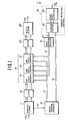
- the video signal reproducing system includes a demultiplexing circuit 11 converting a serial input signal V in derived by reproducing video signal data recorded on a magnetic video tape 1 into parallel data signals.
- the converted parallel data is conducted from the demultiplexing circuit 11 to a latching circuit 12.
- the system has first, second and third field memories 13, 14 and 15, which serve as image data memories and together form a single video signal memory 16.
- the first, second and third field memories 13, 14 and 15 are connected to receive the latched parallel data from the latching circuit 12 as image data.
- the field memories 13, 14 and 15 of the video signal memory 16 are also connected to receive a control input from a write address counter 17 which generates a write address signal S l identifying the next address in the video signal memory 16 to be used for storage.
- the field memories 13, 14 and 15 are controlled by the write address signal S l to store the image data from the latching circuit 12 in a memory area starting at the address identified by the write address signal.
- the write address counter 17 is connected to receive an input from a memory switching control circuit 18 which includes an address control circuit 19.
- the address control circuit 19 supplies an address load signal S 2 to the write address counter 17.
- the address load signal S 2 specifies a loading address.
- the write counter 17 periodically increments the loading address in order to derive the write address signal for supply in response to a reproduction locking signal S 3 from the demultiplexing circuit 11.
- the first, second and third field memories 13, 14 and 15 are also connected to receive a control input from a read address counter 21, specifically to receive a read address signal S 4 which identifies the next address in the memory 16 to be accessed for data retrieval.
- the field memories 13, 14 and 15 respond to the read address signal S4 from the read address counter 21 by retrieving the image data recorded in the memory area starting at the address specified by the read address signal S 4 .
- the read address counter 21 is, in turn, connected to receive an input from the address control circuit 19 in the memory switching control circuit 18 to receive an address load signal 5S.
- the read counter 21 increments or decrements a loading address specified by the address load signal S S .
- the counter value of the read address counter 21 specifies which of the first, second and third field memories 13, 14 and 15 is to be accessed.
- the image data retrieved from the appropriate field memories 13, 14 or 15 of the video signal memory 16 in response to the read address signal S s from the read address counter 21 is fed to a multiplexing circuit 23 via a latching circuit 22.
- the multiplexing circuit 23 converts the parallel data latched by the latching circuit 22 into a serial reproduced video output signal V out .
- the memory switching control circuit 18 generally selects one of the first, second and third field memories 13, 14 and 15 in accordance with a memory-management mode selected on the basis of the data recorded on the magnetic video tape 1 which depends upon the reproduction mode and drive direction selected manually via a control panel (not shown).
- a scanning mode detecting circuit 24 connected for output to the address control circuit 19 supplies a signal identifying the current reproduction mode.
- the video magnetic tape 1 to which the preferred embodiment of the video signal reproducing system of the invention is applied has a plurality of helical tracks A to J.
- each group of helical tracks A to J covers one field of image data.
- the track A is adjacent to the track J of the preceding group of tracks.
- the track A will be referred to hereafter as the "leading boundary track” and the track J will be referred to as the "trailing boundary track”.
- each group of tracks consisting of the tracks A to J will be referred to hereafter as a "record area”.
- the record areas covering odd-numbered fields will be referred to as “odd number record areas” and those covering even-numbered fields will be referred to as "even number record areas”.
- odd number record areas and even number record areas alternate along the tape with each leading boundary track A adjoining the trailing boundary track J of the preceding record area.
- the scanning mode detecting circuit 24 includes a boundary track detecting circuit 31.
- the boundary track detecting circuit 31 detects when the rotary head is scanning one of the boundary tracks A or J.
- the boundary track detecting circuit 31 includes a first detector circuit 32 having D flip-flop circuits D 11 and D 12 .
- the first detector circuit 32 is responsive to a first detecting pulse OS produced when the head moves across the leading boundary track A of the odd number record area RE I .
- the boundary track detecting circuit 31 also includes a second detector circuit 33 having D flip-flop circuits D 21 and D 22 .
- the second detector circuit 33 is responsive to a second detecting pulse OE produced when the head moves across the trailing boundary track J of the odd number record area RE I .
- the boundary track detecting circuit 31 further includes a third detector circuit 34 having D flip-flop circuits D 31 and D 32 .
- the third detector circuit 34 is responsive to a third detecting pulse ES produced when the head moves across the leading boundary track A of the even number record area RE 2 .
- the boundary track detecting circuit 31 further includes a fourth detector circuit 35 having D flip-flop circuits D41 and D 42 .
- the fourth detector circuit 35 is responsive to a fourth detecting pulse EE produced when the head moves across the trailing boundary track J of the even number record area RE 2 .
- the detecting pulses OS and OE are produced by a detector circuit (not shown) when it detects an address code of Figure 2A recorded in the leading track A of an odd number record area RE I . Therefore, the detecting pulses OS and OE are produced every time the head moves across the leading track A of an odd number record area RE 1 .
- the phase of the detecting pulses OS and OE shifts through every cycle of the head rotation relative to the head position, as represented by a head position
- the detecting pulses occur in order of the first detecting pulse OS, the second detecting pulse OE, the first detecting pulse ES and the fourth detecting pulse EE.
- the order of occurrence of the detecting pulses is reversed, since the reproducing head moves from the trailing boundary track J towards the leading boundary track A in each record area. Therefore, during reverse driving of the reproducing head, the detecting pulses occur in the following order; the fourth detecting pulse EE, the third detecting pulse ES, the second detecting pulse OE and the first detecting pulse OS.
- the D flip-flop circuits D 11 and D12 each have a preset terminal PR receiving the first detecting pulse OS.
- the flip-flop circuits D 11 and D12 are set in response to the first detecting pulse OS.
- the PG signal is applied to the flip-flop circuits D 11 and D12 as a trigger signal.
- the flip-flop circuit D 11 is triggered by the PG signal and reset by a logical-0 input at its D-terminal.
- the D-terminal of the flip-flop circuit D 12 is connected to the Q-terminal (set output terminal) of the flip-flop circuit D 11 . Therefore, the flip-flop circuit D 12 is reset when the flip-flop circuit D 11 is reset.
- the output at the Q-terminal of the flip-flop circuit D 12 drops to logical-0 in response to the first pulse of the first detecting signal OS.
- the detecting pulses OS-EE are all inverse-logic pulses.
- the output at the a-terminal returns to logical 1 in response to two successive second PG signal pulses: the output at the Q-terminal of the flip-flop circuit D 12 will be hereafter referred to as the "first detector output OSG".
- the second, third and fourth detector circuits 33, 34 and 35 supply the second, third and fourth detector outputs OEG, ESG and EEG through respective Q -terminals of the flip-flop circuits D 22 , 032 and D 42 , in response to the PG signal.
- Each of the second, third and fourth detector outputs OEG, ESG and EEG varies in substantially the same manner as set out with respect to the first detector output OSG. Specifically, each of the second, third and fourth detector outputs OEG, ESG and EEG drops to the logical-0 level in response to the first pulse of corresponding detecting signal OE, ES and EE and returns to the logical-I level In response to two successive PG signal pulses.
- the Q-terminals of the second-stage flip-flop circuits D 12 , D 22 , D 32 and D 42 of the first to fourth detector circuits 32, 33, 34 and 35 are connected to supply an output to a switching circuit 41.
- the switching circuit 41 is, in turn, connected to an odd number field scan detecting circuit 42 and an even number field scan detecting circuit 43.
- the odd number field scan detecting circuit 42 and the even number field scan detecting circuit 43 comprise D-flip-flop circuits.
- the switching circuit 41 is also connected to receive a forward/reverse switching signal FR from a manually operable forward/reverse switch which controls the switch position of the switching circuit 41.
- the switching circuit 41 supplies set signals ST 1 and ST 2 in response to the first and third detector outputs OSG and ESG, and supplies reset signals RT 1 and RT 2 in response to the first and third detector outputs OSG and ESG, and supplies reset signals RT, and RT 2 in response to the second and fourth detector outputs OEG and EEG, when the switching signal FR is at a level indicative of forward drive.
- the set signals ST I and ST 2 are supplied from the switching circuit 41 to present terminals RP of the flip-flop circuits 42 and 43 serving respectively as the odd number field scan detector circuit 42 and the even number field scan detector circuit 43.
- the switching circuit 41 supplies the reset signals RT 1 and RT 2 to trigger inputs of the flip-flop circuits 42 and 43.
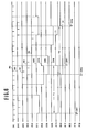
- the flip-flop circuit of the odd number field scan detector circuit 42 is set in response to trailing edges of HIGH-level first detector output pulses OSG and is reset by the constant logical-0 input at its D-terminal in response to the leading edge of the HIGH-level second detector output OEG. Therefore, as shown in Figure 6 (D 1 ), the flip-flop 42 supplies through its Q -terminal an odd number field scan indicative signal I 1 which is held at logical-0 value for the period T 1 during which the head scans through the odd number record area RE 1 .
- the flip-flop circuit of the even number field scan detector circuit 43 is set in response to the trailing edge of HIGH-level third detector output pulses ESG and is reset in response to the leading edge of HIGH level fourth detector output EEG. Therefore, as shown in Figure 6 (D 2 ), the output 1 2 at the Q -terminal of the flip-flop 43 is held at logical-0 value for the period T 2 during which the head scans through the even number record area RE 2 .
- the switching circuit 41 supplies the set signal ST 1 and ST 2 in response to the second and fourth detector outputs EG and EEG, and the reset signal RT 1 and RT 2 in response to the first and third detector outputs OSG and ESG.
- the flip-flop circuit 42 is set in response to the trailing edge of the HIGH-level second detector output OEG and reset in response to the leading edge of the first detector output OSG. Therefore, as above, the output 1 1 at the Q-terminal of the flip-flop circuit 42 is held at logical-0 value for the period T 1 during which the head scans in the reverse direction through the odd number record area RE 1 , as shown in Figure 6 (D 1 ).
- the flip-flop circuit 43 is set in response to the trailing edge of the fourth detector output EEG and reset in response to the leading edge of the third detector output ESG.
- the output 1 2 at the Q -terminal of the flip-flop circuit 43 is held at logical-0 value for the period T 2 during which the head scans in the reverse direction through the even number record area RE 2 .
- the time axis progresses from right to left and the detector outputs OSG, OEG, ESG and EEG drop at points coincident with the first pulse of the corresponding detecting pulse OS, OE, ES and EE and remain at logical-0 until the second PS pulse following the last pulse of the corresponding detecting pulse.
- the flip-flop circuits 42 and 43 have inverting output terminals (Q-terminals) through which the logical inverts of the odd number field scan indicative signal I 1 and the even number field scan indicative signal I 2 respectively are supplied, as shown in Figure 6 (E l ) and (E 2 ). These inverted signals I 1 and I 2 are processed by differentiation circuits 44 and 45. The differentiation circuits 44 and 45 respond to the leading edge of the respectively corresponding inverted signal I 1 and I 2 to supply switching pulses CH 1 and CH 2 , during forward drive operation.
- the differentiation circuit 44 and 45 supplies the switching signals CH 1 and CH 2 in response to the trailing edge of the corresponding inverted signals I 1 and I 2 . Therefore, as can be easily appreciated, the differentiation circuit 44 and 45 supplies the switching pulses CH 1 and CH 2 every time the scan switches between an odd number field and an even number field according to change of the logical level of the input from the flip-flop circuits 42 and 43 as set forth above.
- the switching pulses CH and CH 2 are supplied to a NAND gate 51 which is, in turn, connected to supply outputs to a memory selection switching circuit 52 and a memory switching disabling circuit 53.
- the gate signal of the NAND gate 51 serves as a trigger signal for the memory selection switching circuit 52 and the memory switching disabling circuit 53.
- the Q-terminals of the flip-flops 42 and 43 are connected to an exclusive-OR gate 55 which serves as a disabling condition detector.
- the memory selection switching circuit 52 selects into which of the field memories 13, 14 and 15 the odd number and even number field image data from the reproducing head are to be stored.
- the memory selection switching circuit 52 similarly serves to specify from which of the field memories 13, 14 and 15 recorded image data are to be retrieved.
- the memory selection switching circuit 52 is also connected to the manually operable forward/reverse switch to receive the forward/reverse switching signal FR as an up/down control signal.
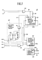
- the circuit 52 includes an up/down counter 52a to increment and decrement the memory selection code. These changes in the up/down counter 52a are controlled in accordance with the forward/reverse switching signal FR. That is, the up/down counter 52a increments the memory selection code during the forward drive operation and decrements it during reverse drive operation.
- the resultant counter value of the up/down counter 52a is fed to a load address converter circuit 54. As shown in Figure 7, the counter value is supplied in the form of three binary signals QC, QB and QA, making up a 3- bit code. Therefore, the load address converter circuit 54 receives QC, QB and QA as counter value indicative data.
- the load address converter circuit 54 derives a writing address load signal S 2 on the basis of the 3-bit counter output QC, QB and QA.
- the write address load signal S 2 is supplied to the write address counter 17 as mentioned previously.
- the load address converter circuit 54 also derives a read address load signal S 5 on the basis of QC, QB and QA to identify which of the field memories 13, 14 and 15 to access.
- the read address load signal s 5 is fed to the read address counter 21.
- the load address converter circuit 54 also receives an odd/even field indicative signal OES recorded on the video tape and picked up by the reproducing head 2.
- the load address converter circuit 54 further includes ROM 54a storing a look-up table scheduling access to of the field memories 13, 14 and 15.
- the look-up table stored in ROM 54a is as follows: Values for the signals S2 and S5 are found in the table in the ROM 54a in terms of the code signal values QA, QB and QC and the odd/even field indicative signal OES.
- the load address converter circuit 54 when the number represented by the code signal QC, QB and QA is "010", and the odd/even field indicative signal OES indicates scanning of the odd number field only, the load address converter circuit 54 generates a write address load signal identifying the first field memory 13 and a read address load signal S 5 identifying the third field memory 15, as shown in Figure 8. In response to the write address load signal S 2 and the read address load signal S 5 thus derived, the image data is stored in the first field memory 13 and recorded image data in the third field memory 15 is read out. On the other hand, when the code signal is "010" and the odd/even field indicative signal OES indicates scan of both odd and even-numbered fields, the write address load signal S 2 specifies both of the first and second field memories 13 and 14.
- the read address load signal S 5 specifies the third field memory 15.
- the image data for the odd number field is stored in the first field memory 13 and the even number field image data is stored in the second field memory 14.
- the image data recorded in the field memory 15 is read out, at the same time.
- the image data recorded in the third field memory 15 is, at this time, reproduced on a video monitor.
- the switching pulse CH I and CH 2 is produced.
- the memory selection switching circuit 52 is responsive to the switching pulses CH, and CH 2 , to increment or decrement the code signal QA, QB and QC in a predetermined order according to the forward/reverse drive identified by the forward/reverse indicative signal FR. Therefore, in the above example, the memory selection switching circuit 52 supplies the code signals QC, QB and QA reading "011" in response to the switching pulses CH 1 and CH 2 .
- the even field image data would be stored in the second field memory 14 and the odd number field image data would be stored in the field memory 15.
- the first field memory 13 would be accessed for the previously stored image data.
- the memory selection switching circuit 52 increments or decrements the up/down counter value in response to each switching pulse CH 1 and CH 2 to update the read/write states of the first, second and third field memory 13, 14 and 15.
- the field memories 13, 14 and 15 are selectively designated for storage of image data according to the order determined by the loop-up table in ROM 54a of the load address converting circuit 54.
- the field memory to which writing in the image data is finished is subsequently accessed for the previously stored image data.
- the code signal value may shift, during forward drive operation, in the table sequence "010", “011” ... “111", “010".
- the code signal value may shift through the reverse order: “010", “111”, “110” ... "010". The order of selection of the field memories 13, 14 and 15 for image data storage and image data retrieval is reversed when the head drive direction is reversed.
- the second field memory 14 in which the even number field data is all stored before the next switching pulse CH 1 or CH2, is next accessed for retrieval of the stored image data.
- the memory selection switching circuit 52 and the load address converter circuit 54 together form the address control circuit 19 in conjunction with the memory switching disabling circuit 53.
- the memory switching disabling circuit 53 disables the switching operation of the memory selection switching circuit 52.
- the memory switching disabling circuit 53 comprises a counter 53a clocked by the output of the NAND circuit 51.
- the memory switching disabling circuit 53 also has a load data input terminal LA which is directly connected for input from the exclusive-OR gate 55, and another load data input terminal LB which is connected for input from the exclusive-OR gate 55 through an inverter 56.
- the exclusive-OR gate 55 receives the odd-numbered field indicative Q-terminal output I 1 and the even number field indicative Q-terminal output 1 2 as condition inputs. On the basis of the condition inputs, the exclusive-OR date 55 supplies a condition signal IH to the load data input terminal LA and inverted load condition signal IH to the load input terminal LB through the inverter 56.
- the disabling circuit derives disabling conditions according to the following table.
- the memory switching disabling circuit 53 also has a load input LOAD which is connected to receive an input from a switching timing detector circuit 57 as a detector signal CT.
- the switching timing detector circuit 57 generally comprises a pair of D-flip-flops D 51 and D 52 .
- the D-flip - flop D51 receives the switching signal FR at its D-terminal.
- the Q-terminal of the flip-flop D 51 is connected to the D-terminal of the second-stage flip-flop D 52 .
- the Q-terminal of the first-stage flip-flop D 51 is connected to one input of an exclusive-OR gate EX. To the other input of the exclusive-OR gate EX, the Q-terminal of the second-stage flip-flop 052 is connected.
- the exclusive-OR gate EX derives the logical sum of the outputs from the flip-flops D51 and D 52 .
- the logical sum derived by the exclusive-OR gate EX serves as the detector signal CT of the switching timing detector circuit 57.
- the detector signal CT drops to logical 0 from logical 1 when the switching signal FR switches state.
- the trailing edge of the logical-1 detector signal CT triggers the memory switching disabling circuit 53 to sample the values at its load data inputs LA and LB.
- the load data "1:0” or “0:1” are read from the load data inputs LA and LB.
- the memory switching disabling circuit 53 is then responsive to the output of the NAND gate 51 produced in response to the switching pulses CH 1 and CH 2 . Assuming that the inputs through the load data inputs LA and LB are "1:0", the memory switching disabling circuit 53 supplies a carrier signal CA after two successive inputs from the NAND gate 51. On the other hand, assuming the load data inputs LA and LB are "0:1", then the memory switching disabling circuit 53 supplies the carrier signal CA after the next input from the NAND gate 51.
- the carrier signal CA is supplied to the memory selection switching circuit 52 via an inverter 58 and serves as an enabling signal for the memory selection switching circuit 52.
- the memory selection switching circuit 52 can increment or decrement the memory selection code.
- the memory switching disabling circuit 53 is held in this condition until the next detector signal CT is received from the switching timing detector circuit 57.
- the memory selection switching circuit 52 when the head drive is reversed while the reproducing head is scanning both an odd number record area and an even number record area, the memory selection switching circuit 52 is disabled until two switching pulses CH 1 and CH 2 are received. On the other hand, when the head drive is reversed while the reproducing head is scanning only one of the odd number and even number record areas, the memory selection switching circuit 52 is disabled until the next single switching pulse CH I or CH 2 .
- the memory selection switching circuit 52 of the address control circuit 19 supplies the memory selection code QC, QB and QA as described previously.
- This memory selection code is labelled "SELECTION CODE” in Figure 8.
- the memory selection code follows the sequence "100”, “101”, “110”, “111”, “010", "011".
- the memory selection switching circuit 52 supplies the memory selection code to the load address converter circuit 54 to designate one or two of the field memories 13, 14 and 15 for storage of the image data contained in the reproduction input signal Vin and the remaining field memory 13, 14 or 15 for access to and reproduction of the previously stored image data.
- the memory selection code is "011", and therefore, the image data from the record area O 11 is stored in the third field memory 15.
- the image data in the record area E 10 is stored in the second field memory 14, as shown in the TABLE I.
- the memory selection code changes to "100". Therefore, the third field memory 15 is continuously designated for storage of the image data from the record area O 11 .
- the second field memory 14 is designated for access to the stored image data.
- the reproduction input data Vin starts to include image data from both the odd number record area O 11 and the even number record area E 11 .
- the first field memory 13 is designated for storage of the image data from the record area E 11 .
- the switching pulse CH 1 or CH2 is supplied from one of the differentiation circuits 44 and 45.
- the memory selection switching circuit 52 increments the switching pulse so that the memory selection code becomes "101".
- the first field memory 13 is still used to store the image data from the even number record area E ll .
- the third field memory 15 is designed for retrieval of stored image data from the record area O 11 .
- the image data read from the third field memory 15 is supplied as the reproduction output Vout.
- the memory selection code in response to each switching pulse CH I or CH 2 , the memory selection code is incremented by one while the video tape 1 is driven forward. Incrementing the memory selection code reallocates the field memories for storage and retrieval of image data. Of course, the image data to be read out of field memory is the same image data stored in the last storage operation.
- the switching timing detector circuit 57 is triggered by the forward/reverse switching signal FR to supply the detector signal CT to the memory switching disabling circuit 53.
- the inputs I I and I 2 to the exclusive-OR gate 55 are "0:0". Therefore, the load data inputs LA and LB are "1:0".
- the memory switching disabling circuit 53 supplies a disabling signal to the memory selection switching circuit 52 through the inverter 58.
- the memory selection switching circuit 52 is disabled until the next switching pulse CH 1 or CH 2 .
- the second field memory 14 is still designated for storage of image data contained in the reproduction input signal Vin.
- the first field memory 13 is designated for retrieval of image data.
- the switching pulse CH 1 or CH 2 is supplied to the memory section switching circuit 52 and the NAND circuit 51 supplies a pulse to the memory switching disabling circuit 53. Since the load data input LA and LB read "1:0", the memory switching disabling circuit 53 responds to the NAND circuit output by supplying the carrier signal CA to the memory selection switching circuit 52. As a result, the memory selection switching circuit 52 is enabled to decrement the switching pulses CH I and CH 2 .
- the reproducing head As it approaches the loading boundary track A of the record area E 13 , starts scanning across the tracks in the record area 0 13 .
- the memory selection code in the memory selection switching circuit 52 remains "011". Therefore, the third memory 15 is newly designated for storage of the image data from the record area 0 13 . Also, the first field memory 13 continues to be accessed for retrieval of image data.
- the switching pulse CH 1 or CH 2 is again supplied to the memory selection switching circuit 52.
- the memory selection switching circuit 52 decrements the . switching pulse CH 1 or CH 2 .
- Figure 9 illustrates the situation in which the tape drive is reversed from forward to reverse while the reproducing head is scanning both an odd number record area 0 13 and an even number record area E 12 .
- the switching timing detecting circuit 57 produces the detector signal CT in response to the forward/reverse switching signal FR.
- the memory switching disabling circuit 53 is responsive to the detector signal CT to read the load data input LA and LB.
- the load data inputs LA, LB are of the combination "0:1”
- the memory switching disabling circuit 53 supplies a disabling signal to the memory selection switching circuit 52 to disable counting operation of the latter for two occurrences of the switching pulses CH 1 or CH 2 .
- the memory selection switching circuit 52 will not respond to the next two switching pulses CH 1 or CH 2 . Since the memory selection code at the moment of reversal of the tape drive was "010", this code value is maintained until the third successive switching pulse CH 1 or CH 2 .
- the third field memory 15 since the third field memory 15 was being accessed for retrieval of image data when the forward/reverse switching signal FR arose, it continues to be accessed until the third switching pulse CH 1 or CH 2 is received. During this period, the second field memory 14 is used for storage of image data from the record area E 13 and the first field memory 13 is used for storage of image data from the record area 0 13 . After completion of the scan of the record area E13, the first switching pulse CH 1 or CH2 is supplied to the memory selection switching circuit 52 and also to the memory switching disabling circuit 53 through the NAND gate 51. However, since the memory selection remains disabled, the memory selection code remains "010".
- the image data in the record area O 1 continues to be stored in the first field memory 13 and image data stored in the third field area 15 continues to be retrieved for video reproduction.
- the image data to be read out during this period is the image data from the record area E 12 stored before reversal of the tape drive direction.
- the reproducing head reaches the boundary between the record areas 013 and E 12 and starts to pick up image data from both record areas.
- the image data from the record area E 12 is stored in the second field memory 14, at this time.
- the second switching pulse CH 1 or CH 2 is supplied.
- the memory switching disabling circuit 53 is triggered to supply the carrier signal CA.
- the memory selection switching circuit 52 is responsive to the carrier signal CA received via the inverter 58 to return to its enabled state.
- the image data from the record area E12 continues to be stored in the second field memory 14. Also, the image data from the record area E 12 stored in the third field memory 15 continues to be retrieved.
- the third switching pulse CHI or CH 2 is produced.
- the memory selection switching circuit 52 decrements the memory selection code to "111" in response to the third switching pulse CH 1 or CH 2 .
- the first field memory 13 is designated for storage of image data from the record area O 12 .
- the second field area now holding image data from the record area E 12 , is designated for retrieval. Therefore, the video image reproduced on the video monitor remains unchanged.
- video image data are scanned, stored, retrieved and reproduced in the same manner as explained with respect to forward tape drive.
- the only difference is the order of update of the memory selection code, which is the reverse of that in forward tape drive.
Landscapes
- Engineering & Computer Science (AREA)
- Multimedia (AREA)
- Signal Processing (AREA)
- Television Signal Processing For Recording (AREA)
- Signal Processing For Digital Recording And Reproducing (AREA)
- Signal Processing Not Specific To The Method Of Recording And Reproducing (AREA)
Priority Applications (1)
| Application Number | Priority Date | Filing Date | Title |
|---|---|---|---|
| AT85302961T ATE68652T1 (de) | 1984-04-28 | 1985-04-26 | Verfahren und geraet zum wiedergeben von aufgezeichneten videosignalen. |
Applications Claiming Priority (2)
| Application Number | Priority Date | Filing Date | Title |
|---|---|---|---|
| JP59087531A JPS60231977A (ja) | 1984-04-28 | 1984-04-28 | 映像信号再生装置 |
| JP87531/84 | 1984-04-28 |
Publications (3)
| Publication Number | Publication Date |
|---|---|
| EP0160539A2 true EP0160539A2 (de) | 1985-11-06 |
| EP0160539A3 EP0160539A3 (en) | 1988-06-01 |
| EP0160539B1 EP0160539B1 (de) | 1991-10-16 |
Family
ID=13917571
Family Applications (1)
| Application Number | Title | Priority Date | Filing Date |
|---|---|---|---|
| EP85302961A Expired - Lifetime EP0160539B1 (de) | 1984-04-28 | 1985-04-26 | Verfahren und Gerät zum Wiedergeben von aufgezeichneten Videosignalen |
Country Status (7)
| Country | Link |
|---|---|
| US (1) | US4751589A (de) |
| EP (1) | EP0160539B1 (de) |
| JP (1) | JPS60231977A (de) |
| AT (1) | ATE68652T1 (de) |
| AU (1) | AU580052B2 (de) |
| CA (1) | CA1305553C (de) |
| DE (1) | DE3584384D1 (de) |
Cited By (4)
| Publication number | Priority date | Publication date | Assignee | Title |
|---|---|---|---|---|
| EP0228784A3 (en) * | 1985-11-06 | 1988-06-01 | Sony Corporation | Video replay store for a multichannel digital video tape recorder |
| EP0241130A3 (en) * | 1986-04-11 | 1989-06-07 | Ampex Corporation | Apparatus for deskewing successively occurring blocks ofapparatus for deskewing successively occurring blocks of data data |
| EP0325256A3 (de) * | 1988-01-22 | 1992-03-11 | Sony Corporation | Gerät zum Wiedergeben von digitalen Videosignalen |
| US5187617A (en) * | 1988-01-22 | 1993-02-16 | Sony Corporation | Apparatus for reproducing digital video signal |
Families Citing this family (13)
| Publication number | Priority date | Publication date | Assignee | Title |
|---|---|---|---|---|
| NL8401404A (nl) * | 1984-05-03 | 1985-12-02 | Philips Nv | Televisiesignaalgeheugen-inschrijfschakeling. |
| US4914527A (en) * | 1986-04-09 | 1990-04-03 | Sony Corporation | Recording and reproducing digital video and audio signals together with a time code signal which is within user control words of the audio data |
| NL8601182A (nl) * | 1986-05-12 | 1987-12-01 | Philips Nv | Werkwijze en inrichting voor het opnemen en/of weergeven van een beeldsignaal en een bijbehorend audiosignaal in respektievelijk van een registratiedrager, en een registratiedrager verkregen volgens de werkwijze. |
| US5016119A (en) * | 1987-02-27 | 1991-05-14 | Sony Corporation | Video signal reproducing apparatus with two modes of keeping track of address |
| JP2774158B2 (ja) * | 1988-10-14 | 1998-07-09 | 三星電子株式会社 | Vtrシステムの画面アンコール方法 |
| EP0402135A3 (de) * | 1989-06-08 | 1992-09-09 | Kabushiki Kaisha Toshiba | Bildwiedergabevorrichtung und -verfahren |
| JPH0322687A (ja) * | 1989-06-19 | 1991-01-31 | Sharp Corp | デジタル記録再生装置 |
| JPH04263588A (ja) * | 1991-02-19 | 1992-09-18 | Matsushita Electric Ind Co Ltd | ディジタルvtr |
| GB2269929B (en) * | 1992-08-21 | 1996-05-22 | Sony Broadcast & Communication | Controlling video replay stores |
| US5398143A (en) * | 1992-12-01 | 1995-03-14 | Samsung Electronics Co., Ltd. | Data placement on tape for a digital video tape recorder suitable for high speed picture playback |
| JP3718375B2 (ja) * | 1999-06-30 | 2005-11-24 | シャープ株式会社 | 記録再生装置 |
| US6915167B2 (en) | 2001-01-05 | 2005-07-05 | Medtronic, Inc. | Method and apparatus for hardware/firmware trap |
| US6925331B2 (en) * | 2002-09-30 | 2005-08-02 | Medtronic, Ind. | EGM signal acquisition and processing system |
Family Cites Families (9)
| Publication number | Priority date | Publication date | Assignee | Title |
|---|---|---|---|---|
| US4000510A (en) * | 1975-06-02 | 1976-12-28 | Ampex Corporation | System for storage and retrieval of video information on a cyclical storage device |
| JPS5614787A (en) * | 1979-07-18 | 1981-02-13 | Sony Corp | Video signal reproduction system |
| US4511931A (en) * | 1980-07-28 | 1985-04-16 | Eastman Kodak Company | Slow motion using longitudinal recording and forward/reverse tape transportation |
| US4361849A (en) * | 1980-11-06 | 1982-11-30 | Rca Corporation | Video disc vari-speed playback system |
| GB2098021B (en) * | 1981-05-06 | 1985-06-19 | Sony Corp | Digital television apparatuses |
| AU526332B2 (en) * | 1981-05-26 | 1983-01-06 | Victor Company Of Japan Limited | Slow motion and still picture reproduction |
| JPS58164383A (ja) * | 1982-03-25 | 1983-09-29 | Sony Corp | ビデオ信号記録装置 |
| JPS5954388A (ja) * | 1982-09-22 | 1984-03-29 | Victor Co Of Japan Ltd | デイジタルビデオ信号再生装置 |
| US4538377A (en) * | 1983-10-06 | 1985-09-03 | Thornton Ken O | Irrigation system |
-
1984
- 1984-04-28 JP JP59087531A patent/JPS60231977A/ja active Granted
-
1985
- 1985-04-25 US US06/727,381 patent/US4751589A/en not_active Expired - Lifetime
- 1985-04-25 CA CA000480038A patent/CA1305553C/en not_active Expired - Lifetime
- 1985-04-26 DE DE8585302961T patent/DE3584384D1/de not_active Expired - Lifetime
- 1985-04-26 EP EP85302961A patent/EP0160539B1/de not_active Expired - Lifetime
- 1985-04-26 AU AU41707/85A patent/AU580052B2/en not_active Ceased
- 1985-04-26 AT AT85302961T patent/ATE68652T1/de not_active IP Right Cessation
Cited By (5)
| Publication number | Priority date | Publication date | Assignee | Title |
|---|---|---|---|---|
| EP0228784A3 (en) * | 1985-11-06 | 1988-06-01 | Sony Corporation | Video replay store for a multichannel digital video tape recorder |
| US4803567A (en) * | 1985-11-06 | 1989-02-07 | Sony Corporation | Video replay store for a multi-channel digital video tape recorder |
| EP0241130A3 (en) * | 1986-04-11 | 1989-06-07 | Ampex Corporation | Apparatus for deskewing successively occurring blocks ofapparatus for deskewing successively occurring blocks of data data |
| EP0325256A3 (de) * | 1988-01-22 | 1992-03-11 | Sony Corporation | Gerät zum Wiedergeben von digitalen Videosignalen |
| US5187617A (en) * | 1988-01-22 | 1993-02-16 | Sony Corporation | Apparatus for reproducing digital video signal |
Also Published As
| Publication number | Publication date |
|---|---|
| AU580052B2 (en) | 1988-12-22 |
| JPS60231977A (ja) | 1985-11-18 |
| EP0160539B1 (de) | 1991-10-16 |
| AU4170785A (en) | 1985-10-31 |
| CA1305553C (en) | 1992-07-21 |
| US4751589A (en) | 1988-06-14 |
| ATE68652T1 (de) | 1991-11-15 |
| EP0160539A3 (en) | 1988-06-01 |
| JPH0533597B2 (de) | 1993-05-19 |
| DE3584384D1 (de) | 1991-11-21 |
Similar Documents
| Publication | Publication Date | Title |
|---|---|---|
| US4751589A (en) | Method and apparatus for reproducing recorded video signal | |
| RU2073913C1 (ru) | Носитель записи, способ и устройство для записи информационных файлов и устройство для воспроизведения информации с такого носителя записи | |
| US4195317A (en) | Video recording and playback editing system with displayed cue signals | |
| CS254952B2 (en) | Information disk's optical reader | |
| NL8005526A (nl) | Inrichting voor weergave van gedigitaliseerde informatie, meer in het bijzonder van een in meerkanalig digitale vorm gebracht videosignaal. | |
| CA2019080C (en) | Method and apparatus for reproducing a digital video signal | |
| RU2051428C1 (ru) | Устройство для воспроизведения информации с носителя записи и носитель записи для использования в таком устройстве | |
| US5179451A (en) | Method and device for signal reproduction used in a digital signal reproduction apparatus | |
| EP0753854A2 (de) | Datenaufzeichnungsgerät und Datenwiedergabegerät | |
| EP0153410B1 (de) | Vorrichtung zum aufzeichnen und wiedergeben von signalen | |
| EP0559426B1 (de) | Steuervorrichtung zur Bildsuche für einen digitalen Videobandrecorder | |
| US4905099A (en) | Intermediate picture field storage system for variable speed magnetic tape video data read-out | |
| EP0341790A2 (de) | Magnetbandwiedergabemethode und -gerät mit rotierendem Trommelkopf | |
| US5329366A (en) | Time base corrector for video signal | |
| US5469269A (en) | High speed optical information system and method | |
| US5253119A (en) | Digital image reproduction apparatus and method | |
| US5862294A (en) | Video signal reproducing apparatus in image fast locking system | |
| US5079637A (en) | Apparatus for reproducing color video signal recorded by TCI signal format | |
| KR960005399B1 (ko) | 헬리컬 스캐닝 기록방식 비디오 레코더 | |
| EP0584925B1 (de) | Steuergerät für Videowiedergabespeicher | |
| EP0473416A2 (de) | Videosignalwiedergabegerät | |
| EP1005226A2 (de) | MPEG Wiedergabe-Anlage und -Verfahren | |
| JP3099239B2 (ja) | 再生装置および方法 | |
| SU1126999A1 (ru) | Устройство дл магнитной записи | |
| KR950000878Y1 (ko) | 멀티 화면 기록시스템 |
Legal Events
| Date | Code | Title | Description |
|---|---|---|---|
| PUAI | Public reference made under article 153(3) epc to a published international application that has entered the european phase |
Free format text: ORIGINAL CODE: 0009012 |
|
| AK | Designated contracting states |
Designated state(s): AT DE FR GB NL |
|
| PUAL | Search report despatched |
Free format text: ORIGINAL CODE: 0009013 |
|
| AK | Designated contracting states |
Kind code of ref document: A3 Designated state(s): AT DE FR GB NL |
|
| 17P | Request for examination filed |
Effective date: 19881021 |
|
| 17Q | First examination report despatched |
Effective date: 19900806 |
|
| GRAA | (expected) grant |
Free format text: ORIGINAL CODE: 0009210 |
|
| AK | Designated contracting states |
Kind code of ref document: B1 Designated state(s): AT DE FR GB NL |
|
| REF | Corresponds to: |
Ref document number: 68652 Country of ref document: AT Date of ref document: 19911115 Kind code of ref document: T |
|
| REF | Corresponds to: |
Ref document number: 3584384 Country of ref document: DE Date of ref document: 19911121 |
|
| ET | Fr: translation filed | ||
| PLBE | No opposition filed within time limit |
Free format text: ORIGINAL CODE: 0009261 |
|
| STAA | Information on the status of an ep patent application or granted ep patent |
Free format text: STATUS: NO OPPOSITION FILED WITHIN TIME LIMIT |
|
| 26N | No opposition filed | ||
| REG | Reference to a national code |
Ref country code: GB Ref legal event code: IF02 |
|
| PGFP | Annual fee paid to national office [announced via postgrant information from national office to epo] |
Ref country code: FR Payment date: 20030408 Year of fee payment: 19 |
|
| PGFP | Annual fee paid to national office [announced via postgrant information from national office to epo] |
Ref country code: AT Payment date: 20030411 Year of fee payment: 19 |
|
| PGFP | Annual fee paid to national office [announced via postgrant information from national office to epo] |
Ref country code: GB Payment date: 20030423 Year of fee payment: 19 |
|
| PGFP | Annual fee paid to national office [announced via postgrant information from national office to epo] |
Ref country code: NL Payment date: 20030429 Year of fee payment: 19 |
|
| PGFP | Annual fee paid to national office [announced via postgrant information from national office to epo] |
Ref country code: DE Payment date: 20030508 Year of fee payment: 19 |
|
| PG25 | Lapsed in a contracting state [announced via postgrant information from national office to epo] |
Ref country code: GB Free format text: LAPSE BECAUSE OF NON-PAYMENT OF DUE FEES Effective date: 20040426 Ref country code: AT Free format text: LAPSE BECAUSE OF NON-PAYMENT OF DUE FEES Effective date: 20040426 |
|
| PG25 | Lapsed in a contracting state [announced via postgrant information from national office to epo] |
Ref country code: NL Free format text: LAPSE BECAUSE OF NON-PAYMENT OF DUE FEES Effective date: 20041101 |
|
| PG25 | Lapsed in a contracting state [announced via postgrant information from national office to epo] |
Ref country code: DE Free format text: LAPSE BECAUSE OF NON-PAYMENT OF DUE FEES Effective date: 20041103 |
|
| GBPC | Gb: european patent ceased through non-payment of renewal fee |
Effective date: 20040426 |
|
| PG25 | Lapsed in a contracting state [announced via postgrant information from national office to epo] |
Ref country code: FR Free format text: LAPSE BECAUSE OF NON-PAYMENT OF DUE FEES Effective date: 20041231 |
|
| NLV4 | Nl: lapsed or anulled due to non-payment of the annual fee |
Effective date: 20041101 |
|
| REG | Reference to a national code |
Ref country code: FR Ref legal event code: ST |