EP0160706A1 - Fernsehempfänger - Google Patents
Fernsehempfänger Download PDFInfo
- Publication number
- EP0160706A1 EP0160706A1 EP84904159A EP84904159A EP0160706A1 EP 0160706 A1 EP0160706 A1 EP 0160706A1 EP 84904159 A EP84904159 A EP 84904159A EP 84904159 A EP84904159 A EP 84904159A EP 0160706 A1 EP0160706 A1 EP 0160706A1
- Authority
- EP
- European Patent Office
- Prior art keywords
- video signal
- field
- vertical
- frequency
- signal
- Prior art date
- Legal status (The legal status is an assumption and is not a legal conclusion. Google has not performed a legal analysis and makes no representation as to the accuracy of the status listed.)
- Granted
Links
Images


Classifications
-
- H—ELECTRICITY
- H04—ELECTRIC COMMUNICATION TECHNIQUE
- H04N—PICTORIAL COMMUNICATION, e.g. TELEVISION
- H04N7/00—Television systems
- H04N7/01—Conversion of standards, e.g. involving analogue television standards or digital television standards processed at pixel level
- H04N7/0127—Conversion of standards, e.g. involving analogue television standards or digital television standards processed at pixel level by changing the field or frame frequency of the incoming video signal, e.g. frame rate converter
- H04N7/0132—Conversion of standards, e.g. involving analogue television standards or digital television standards processed at pixel level by changing the field or frame frequency of the incoming video signal, e.g. frame rate converter the field or frame frequency of the incoming video signal being multiplied by a positive integer, e.g. for flicker reduction
-
- Y—GENERAL TAGGING OF NEW TECHNOLOGICAL DEVELOPMENTS; GENERAL TAGGING OF CROSS-SECTIONAL TECHNOLOGIES SPANNING OVER SEVERAL SECTIONS OF THE IPC; TECHNICAL SUBJECTS COVERED BY FORMER USPC CROSS-REFERENCE ART COLLECTIONS [XRACs] AND DIGESTS
- Y10—TECHNICAL SUBJECTS COVERED BY FORMER USPC
- Y10S—TECHNICAL SUBJECTS COVERED BY FORMER USPC CROSS-REFERENCE ART COLLECTIONS [XRACs] AND DIGESTS
- Y10S348/00—Television
- Y10S348/91—Flicker reduction
Definitions
- the present invention relates to a television receiver which displays a television picture at, for example, field frequency twice the normal field frequency.
- interlaced scanning system In the existing television system, a so-called interlaced scanning system is carried out. That is, one picture (frame) is transmitted by two vertical scannings (fields). This interlaced scanning system is considered in order to increase the number of scanning lines as much as possible in a limited frequency band without a flicker being perceived by a viewer.
- the field frequency is 50Hz. By this frequency, the flicker can not be removed completely and the flicker becomes conspicuous particularly when the brightness of the television picture is high.
- a television receiver is proposed that a television picture is displayed at a field frequency twice the normal field frequency.
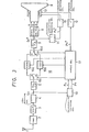
- Fig. 1 shows an example thereof.
- reference numeral 1 designates an antenna, 2 a tuner, 3 a video intermediate frequency amplifier, and 4 a video detecting circuit.
- the video detecting circuit 4 produces a video signal Sv of interlaced system of 625 lines/50 fields and 2 : 1.
- This video signal Sv is converted to a digital signal by an A/D converter 5 and then fed to a converting circuit 6 so as to be converted to a field twice normal speed video signal with field frequency twice the normal field frequency.
- the converting circuit 6 is formed of field memories (random access memories having a storage capacity of picture elements of one field period (IV)) 6a and 6b and switching circuits 6c and 6d.
- the switching circuit 6c is changed in position to the sides of the memories 6a and 6b at every field period IV, while the switching circuit 6d is changed in position reversely.
- the memory selected by the switching circuit 6c is supplied with a write clock pulse having a timing corresponding to the above-described picture elements, while the memory selected by the switching circuit 6d is supplied with a read clock pulse with frequency twice the frequency of the write clock pulse.
- the video signal Sv converted to the digital signal by the A/D converter 5 is supplied through the switching circuit 6c to the memories 6a and 6b by one field each at every field period 1V in which it is written.
- the video signal of one field amount, which is written in the memories 6b and 6a during a field period IV just before the above-mentioned field period, is read out therefrom continuously twice with a cycle of -5 V.
- This video signal is derived through the switching circuit 6d.
- the switching circuit 6d delivers a field twice normal speed video signal Sv' with field frequency.
- This video signal Sv' is converted to an analog signal by a D/A converter 7 and then fed to a signal processing circuit 8. Then, from the signal processing circuit 8, red, green and blue primary color signals R, G and B are produced and then supplied to an image receiving tube 9, respectively.
- the video signal Sv derived from the video detecting circuit 4 is supplied to a vertical synchronizing separating circuit 10.
- a vertical synchronizing signal Pv derived from the separating circuit 10 is multiplied twice by a frequency multiplyer 11 to be a signal with frequency twice the-ordinary frequency. This signal is supplied through a vertical deflecting circuit 12 to a deflecting coil 13.
- the video signal Sv' derived from the D/A converter 7 is supplied to a horizontal synchronizing separating circuit 14.
- a horizontal synchronizing signal P H ' (having the frequency twice the normal frequency) derived from the separating circuit 14 is supplied through a horizontal deflecting circuit 15 to the deflecting coil 13.
- the primary color signals R, G and B each of which has the field frequency twice the normal field frequency are supplied to the picture receiving tube 9 and the horizontal and vertical deflection scannings are carried out at scanning speed twice the normal scanning speed, and hence a color picture with the field frequency twice the normal field frequency is displayed on the picture receiving tube 9. Accordingly, also in the above CCIR system, the field frequency becomes 100Hz which is twice the normal field frequency so that the viewer feels no flicker.
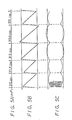
- the write-in state of the video signal Sv derived from the video detecting circuit 4 in the memories 6a and 6b is expressed as shown in Fig. 2A, in which references F l and F 2 designate first and second fields, respectively.
- the video_signal Sv' from the converting circuit 6 is expressed as shown in Fig. 2B.
- arrows represent the positions of the vertical synchronizing signals.
- the phase of the horizontal synchronization is displaced by 180° at every two fields, or at every seconds (shown by broken line arrows), whereby the synchronization on the upper portion of the picture screen is disturbed, resulting in a picture distorion.
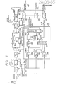
- Fig. 3 shows an example thereof.
- like parts corresponding to those of Fig. 1 are marked with the same references.
- the video signal Sv derived from the video detecting circuit 4 is converted to the digital signal by the A/D converter 5 and then fed to a converting circuit 16 so as to be converted to the field twice normal speed video signal with the frequency twice the normal field frequency.
- the converting circuit 16 is formed of field memories (random access memories) 16a and 16b having storage capacities of picture elements of 313 horizontal periods (313H) and 312 horizontal periods (312H) and switching circuits 16c and 16d.
- the switching circuit 16 is changed in position alternately to the side of the memory 16a during each period of 313H and to the side of the memory 16b during each period of 312H, while the switching circuit 16d is changed in position in the reverse manner.
- These change-over of the change-over switches 16c and 16d are controlled by a control circuit 17.
- This control circuit 17 is supplied with horizontal and vertical synchronizing signals P H and P v which are separated from the video signal Sv by a synchronizing separating circuit 18.
- the memory selected by the switching circuit 16c is supplied with the write clock pulse having the timing corresponding to the above picture elements, while the memory selected by the switching circuit 16d is supplied with a read clock pulse with the frequency twice the frequency of the write clock pulse.
- the video signal Sv converted to the digital signal by the A/D converter 5 is supplied through the switching circuit 16c to the memories 16a and 16b in which it is alternately written during each period of 313H and 312 H .
- Fig. 4A shows the write-in state of the memories 16a and 16b, in which references F 1 and F 2 represent the first and second fields, respectively.
- the video signal written in the other of the memories 16b and 16a during the periods just before the above 312H and 313H are read out therefrom twice continuously.
- This signal is derived through the switching circuit 16d as a field twice normal speed video signal Sv * .
- FIG. 4B shows the video signal Sv * which is derived through the switching circuit 16d, in which the field portions corresponding to those of Fig. 4A are marked with the same references.
- Fig. 4B at the portions of, for example, the F 1 and F 1 fields (the portions read out from the memory 16a), 313 lines are not read out because of a time relation. Further, at, for example, the F 2 and F 2 field portions (the portions read out from the memory 16b), the video signal of one line amount is lacked and during that period, the reading operation is stopped and the video signal of one line amount is lacked (shown by one-dot chain lines). The extra and lack of the video signal of one line amount as mentioned above occur in the vertical blanking period so that in practice, this does not disturb the television picture.
- the writing in and reading out from the memories 16a and 16b are controlled by the control circuit 17.
- the video signal Sv * derived from the switching circuit 16d is converted to the analog signal by the D/A converter 7 and then fed to the signal processing circuit 8. Then, the red, green and blue primary color signals R, G and B are produced from the signal processing circuit 8 and then fed to the picture receiving tube 9, respectively.
- the control circuit 17 produces a vertical synchronizing signal Pv * at the timing shown by arrows in Fig. 4B. More particularly, the vertical synchronizing signal Pv * is produced at the beginning of the first F 1 field, at the timing after 312 lines from the preceding line, namely, at the beginning of the second F 1 field, at the timing after 311.5 lines from the preceding line, at the timing after 313 lines from the preceding line and at the timing after 313.5 lines from the preceding line, or the beginning of the first F 1 field, hereinafter similarly.
- This synchronizing signal Pv * is supplied through the vertical deflecting circuit 12 to the deflecting coil 13 which then carries out the vertical deflection scanning.
- the scanning lines are formed at the same positions and the scanning lines respectively formed at the F 1 field and F 2 field are displaced by scanning line spacing each. In other words, the interlaced relation of the video signal Sv is kept as it is.
- the video signal Sv * from the D/A converter 7 is supplied to the horizontal synchronizing separating circuit 14.
- a horizontal synchronizing signal P H * (having the frequency twice the normal frequency) derived from the separating circuit 14 is supplied through the horizontal deflecting circuit 15 to the deflecting coil 13 by which the horizontal deflection scanning is carried out.
- the horizontal synchronization of the video signal Sv * becomes continuous as shown in Fig. 4B so that the synchronization can be prevented from being disturbed by the insuccessive horizontal synchronization unlike the example of Fig. 1 and thus no picture distortion is produced.
- a parabolic wave current with the vertical synchronizing frequency is superposed on the horizontal deflection current.
- the cycle of the vertical synchronizing signal Pv * is different (see Fig. 5A) as mentioned above, also the vertical deflection current becomes correspondingly different (see Fig. 5B).
- the horizontal deflection current waveform is changed at every vertical cycle (see Fig. 5C).
- a jitter appears in the right and left ends of the picture screen at a fundamental frequency of 25Hz (four field cycles of F 1 , F 1 , F 2 , and F 2 ). This jitter becomes conspicuous much if the deflection angle becomes larger.
- the present invention is to prevent a jitter from being produced at the right and left ends of a picture screen without providing a special deflection correcting circuit.
- the present invention is to change the read clock frequency for a field memory which forms a converting circuit for converting the field frequency at the unit of vertical cycle and to make each vertical cycle of a video signal read out from the field memory substantially equal.
- the horizontal deflecting current waveforms become equal to each other in each vertical cycle so that a jitter can be prevented from being produced at the right and left ends of the picture screen.
- Figs. 1 and 3 are respectively block diagrams showing prior art examples
- Figs. 2, 4 and 5 are respectively diagrams useful for explaining the prior art examples
- Fig. 6_ is a block diagram showing an embodiment of a television receiver according to the present invention
- Fig. 7 is a diagram showing a practical example of a PLL circuit
- Fig. 8 is a block diagram showing another embodiment of the television receiver according to the present invention
- Fig. 9 is a diagram useful for the explanation thereof.
- FIG. 6 An embodiment of a television receiver according to the present invention will hereinafter be described with reference to Fig. 6.
- Fig. 6 like parts correspocding to those of Fig. 3 are marked with the same references and will not be described in detail.
- reference numeral 19 designates a PLL circuit.
- This PLL circuit 19 is supplied with the horizontal synchronizing signal P H from the synchronizing separating circuit 18 and produces at its output side a signal with the frequency of, for example, 1250 f H (f H is the horizontal frequency).
- This signal is supplied through a frequency divider 20 having a frequency dividing ratio of 2 to a write address counter 21 as its write clock pulse.
- a write address W AD from the counter 21 is supplied through a switching circuit 22 to the memories 16a and 16b.
- the PLL circuit 19 is constructed as, for example, shown in Fig. 7.
- reference numerals 27, 28, 29 and 30 designate PLL circuits and they produce read clock pulses CL A , CL B , CL C , and CL D of A, B, C and D fields, respectively.
- These PLL circuits 27 to 30 are supplied with the horizontal synchronizing signal P H from the synchronizing separating circuit 18.
- each frequency of these clock pulses CL A to CL D is selected to be substantially twice the frequency of the write clock pulse.
- the frequencies f A , f B , f C and f D of the clock pulses CL A , CL B , CL C and CL D are selected to be 1248 f H , 1246 f H , 1252 f H and 1254 f H , respectively.
- the clock pulses CL A , CL B , CL C and CL D from these PLL circuits 27, 28, 29 and 30 are respectively supplied to a switching circuit 31 and the switching circuit 31 delivers the clock pulses CL A , CL B , CL C and CL D during the periods of the A, B, C and D fields.
- the clock pulse derived from the switching circuit 31 is supplied to a read address counter 32.
- a read address R AD from the counter 32 is supplied through the switching circuit 22 to the memories 16a and 16b. In this case, of the memories 16a and 16b, the memory set in the write mode by the switching circuit 22 is supplied with the write address WAD' while the memory set in the read mode thereby is supplied with the read address R AD .
- reference numeral' 33 designates a pincushion distortion correcting circuit, by which a parabolic wave current of vertical synchronizing frequency for use in correcting a pincushion distortion is superposed upon the horizontal deflecting current.
- circuit elements are formed similarly to those of the example shown in Fig. 3.
- This embodiment is constructed as mentioned above, in which during the A, B, C and D fields, the different read clock pulses CL A , CL B , CL C and CL D are supplied respectively and the periods of these A, B, C and D fields, or the respective vertical periods become equal to 10 m sec so that the horizontal deflecting current waveform on which the parabolic wave current of the vertical synchronizing frequency for correcting the right and left pincushion distortions in each vertical period is superposed becomes equal, thus removing such a defect that the jitter is produced at the right and left ends of the picture screen unlike the example of Fig. 3. Accordingly, in this embodiment, it is not necessary to provide the special correcting circuit.
- Fig. 8 shows another embodiment of this invention.
- like parts corresponding to those of Fig. 6 are marked with the same references.
- the timing at which the vertical synchronizing signal Pv * is produced is selected to be the timing shown by arrows in Fig. 9. That is, at the timing of the beginning of the first Fi field, at the timing with a delay of 312 lines after the preceding timing, at the timing with the delay of 312.5 lines after the preceding timing, at the timing with a delay of 313 lines after the preceding timing and at the timing with a delay of 312.5 lines after the preceding timing, or at the timing of the beginning of the first F i field and at the similar timing the vertical synchronizing signal Pv * is produced hereinafter.
- reference numerals 34, 35 and 36 respectively designate PLL circuits which produce read clock pulses CL , CL and CL for the periods B'(D'), A' and C'. These PLL circuits 34 to 36 are supplied with the horizontal synchronizing signal P H from the synchronizing separating circuit 18.
- the frequencies f , f and f of the clock pulses CL , CL and CL are respectively selected to be 1250 f H , 1248 f H and 1252 f H .
- the clock pulses CL , CL and CL from these PLL circuits 34, 35 and 36 are respectively supplied to a switching circuit 37 and the switching circuit 37 delivers clock pulses CL , CL and CL during the field periods of B'( D '), A' and C'.
- the clock pulses derived from the switching circuit 37 are supplied to the read address counter 32.
- the clock pulse CL derived from the PLL circuit 34 is supplied through the frequency divider 20 to the write address counter 21 as the write clock pulse therefor.
- circuit elements are formed similarly to those of the example shown in Fig. 6.
- Fig. 8 The embodiment of Fig. 8 is constructed as described above. Accordingly, during the respective B'(D'), A' and C' fields, the different read clock pulses CL , CL and CL are supplied respectively so that the periods of respective A', B', C' and D' fields, or the respective vertical periods become 10 m sec equally. Therefore, the horizontal deflecting current waveforms in the respective vertical periods become equal so that it becomes possible to achieve the similar action and effect to those of the example of Fig. 6.
- the frequencies of the write clock pulse and the read clock pulse are not limited to those of the above-described embodiments but may be, for example, twice the above frequencies. While in the above-mentioned embodiments the interlaced scanning system of the video system of 625 lines/50 fields and 2 : 2 is explained, the present invention is not limited to the above system but can be applied similarly to other interlaced scanning system of the other video signal. While in the above-described embodiments the field frequency is selected to be twice, the present invention is not limited to the above field frequency but can be similarly applied to a case in which the field frequency is changed to be three times, four times,
- the horizontal deflecting current waveform on which the parabolic wave current of, for example, the vertical cycle is superposed becomes equal during each vertical period so that the jitter is not produced at the right and left ends of the picture screen. Accordingly, no such special correcting circuit for removing the jitter is required.
Landscapes
- Engineering & Computer Science (AREA)
- Multimedia (AREA)
- Signal Processing (AREA)
- Television Systems (AREA)
- Details Of Television Scanning (AREA)
- Color Television Systems (AREA)
Applications Claiming Priority (2)
| Application Number | Priority Date | Filing Date | Title |
|---|---|---|---|
| JP208740/83 | 1983-11-07 | ||
| JP58208740A JPS60100887A (ja) | 1983-11-07 | 1983-11-07 | テレビジヨン受像機 |
Publications (3)
| Publication Number | Publication Date |
|---|---|
| EP0160706A1 true EP0160706A1 (de) | 1985-11-13 |
| EP0160706A4 EP0160706A4 (de) | 1986-03-04 |
| EP0160706B1 EP0160706B1 (de) | 1989-02-01 |
Family
ID=16561292
Family Applications (1)
| Application Number | Title | Priority Date | Filing Date |
|---|---|---|---|
| EP84904159A Expired EP0160706B1 (de) | 1983-11-07 | 1984-11-07 | Fernsehempfänger |
Country Status (6)
| Country | Link |
|---|---|
| US (1) | US4651209A (de) |
| EP (1) | EP0160706B1 (de) |
| JP (1) | JPS60100887A (de) |
| AU (1) | AU572592B2 (de) |
| DE (1) | DE3476622D1 (de) |
| WO (1) | WO1985002312A1 (de) |
Families Citing this family (17)
| Publication number | Priority date | Publication date | Assignee | Title |
|---|---|---|---|---|
| GB8429921D0 (en) * | 1984-11-27 | 1985-01-03 | British Telecomm | Flexible regenerator |
| JPS61139174A (ja) * | 1984-12-11 | 1986-06-26 | Sony Corp | 倍速変換装置 |
| GB8608876D0 (en) * | 1986-04-11 | 1986-05-14 | Rca Corp | Television display system |
| JP2526558B2 (ja) * | 1986-10-21 | 1996-08-21 | ソニー株式会社 | ビデオ信号のスキャンコンバ−タ装置 |
| US5249052A (en) * | 1987-02-14 | 1993-09-28 | Canon Kabushiki Kaisha | Image display system with compressed video signal recording and display |
| NL8700903A (nl) * | 1987-04-16 | 1988-11-16 | Philips Nv | Beeldweergeefinrichting met een rastertalomzetter. |
| WO1990000789A1 (fr) * | 1988-07-14 | 1990-01-25 | Seiko Epson Corporation | Circuit de traitement de signaux video |
| US5014128A (en) * | 1989-04-24 | 1991-05-07 | Atronics International Inc. | Video interface circuit for displaying capturing and mixing a live video image with computer graphics on a video monitor |
| JPH0748838B2 (ja) * | 1989-04-27 | 1995-05-24 | 三菱電機株式会社 | テレビ画像表示装置 |
| JP2502829B2 (ja) * | 1991-03-22 | 1996-05-29 | 松下電器産業株式会社 | 画像表示装置 |
| US6469741B2 (en) | 1993-07-26 | 2002-10-22 | Pixel Instruments Corp. | Apparatus and method for processing television signals |
| JPH08228359A (ja) * | 1995-02-22 | 1996-09-03 | Mitsubishi Electric Corp | カラー画像表示装置 |
| US6204889B1 (en) * | 1995-12-15 | 2001-03-20 | Canon Kabushiki Kaisha | Image information processing apparatus |
| JPH1188716A (ja) | 1997-09-03 | 1999-03-30 | Hitachi Ltd | ディスプレイ装置 |
| KR100281885B1 (ko) * | 1998-12-28 | 2001-02-15 | 윤종용 | 디지털 신호 수신장치의 클럭 주파수 변환장치 |
| US6522363B1 (en) * | 1999-07-30 | 2003-02-18 | Thomson Licensing S.A. | Display frame rate adaptation |
| US6894731B2 (en) * | 2001-08-31 | 2005-05-17 | Thomson Licensing S.A. | Raster distortion correction arrangement |
Family Cites Families (8)
| Publication number | Priority date | Publication date | Assignee | Title |
|---|---|---|---|---|
| US4322750A (en) * | 1979-05-08 | 1982-03-30 | British Broadcasting Corporation | Television display system |
| JPS57111176A (en) * | 1980-12-26 | 1982-07-10 | Sony Corp | Television picture receiver |
| NL8100603A (nl) * | 1981-02-09 | 1982-09-01 | Philips Nv | Rasterfrequentieverdubbelingsschakeling voor een televisiesignaal. |
| AU549207B2 (en) * | 1981-02-12 | 1986-01-16 | Sony Corporation | Double-scanning non-interlaced colour television display |
| JPS5879378A (ja) * | 1981-11-05 | 1983-05-13 | Sony Corp | テレビジヨン受像機 |
| JPS5894278A (ja) * | 1981-11-30 | 1983-06-04 | Sony Corp | テレビ受像機 |
| JPS5896460A (ja) * | 1981-12-03 | 1983-06-08 | Sony Corp | テレビ受像機 |
| AU560269B2 (en) * | 1982-09-22 | 1987-04-02 | Philips Electronics N.V. | Field number conversion |
-
1983
- 1983-11-07 JP JP58208740A patent/JPS60100887A/ja active Pending
-
1984
- 1984-11-07 US US06/756,984 patent/US4651209A/en not_active Expired - Fee Related
- 1984-11-07 EP EP84904159A patent/EP0160706B1/de not_active Expired
- 1984-11-07 WO PCT/JP1984/000532 patent/WO1985002312A1/ja not_active Ceased
- 1984-11-07 DE DE8484904159T patent/DE3476622D1/de not_active Expired
- 1984-11-07 AU AU36121/84A patent/AU572592B2/en not_active Ceased
Also Published As
| Publication number | Publication date |
|---|---|
| EP0160706A4 (de) | 1986-03-04 |
| US4651209A (en) | 1987-03-17 |
| AU3612184A (en) | 1985-06-03 |
| WO1985002312A1 (en) | 1985-05-23 |
| DE3476622D1 (en) | 1989-03-09 |
| AU572592B2 (en) | 1988-05-12 |
| EP0160706B1 (de) | 1989-02-01 |
| JPS60100887A (ja) | 1985-06-04 |
Similar Documents
| Publication | Publication Date | Title |
|---|---|---|
| US4651209A (en) | Television display system with increased field frequency | |
| US4249213A (en) | Picture-in-picture television receiver | |
| KR910006295B1 (ko) | 텔레비전 수상기 | |
| JP2502829B2 (ja) | 画像表示装置 | |
| DK165537B (da) | Kompatibelt fjernsynsanlaeg med bred billedskaerm | |
| US4604651A (en) | Television circuit arrangement for field and line frequency doubling and picture part magnification | |
| US4672446A (en) | Television receiver having interlaced scanning with doubled field frequency | |
| US5166801A (en) | Large size display apparatus for high definition television | |
| US4200887A (en) | Television camera | |
| JPS60263139A (ja) | 画像記録装置 | |
| EP0153861A2 (de) | Verzögerungsschaltung für ein Videosignal | |
| US5151786A (en) | Field decision correction apparatus | |
| JPH0436510B2 (de) | ||
| KR100225581B1 (ko) | 영상재생 장치의 분할 화면 출력 제어방법 및 이를 수행하기 위한 장치 | |
| JP3186994B2 (ja) | 画像表示装置 | |
| KR100280848B1 (ko) | 비디오 주사방식 변환회로 | |
| KR960001739B1 (ko) | 광 스크린의 화상 가변 표시장치 | |
| JPH0226482A (ja) | テレビジョン信号変換回路 | |
| JP2699305B2 (ja) | n倍速走査テレビジョン受像機 | |
| JP2711392B2 (ja) | テレビジョン信号の時間軸圧縮装置 | |
| JPH0588598B2 (de) | ||
| JPH0430789B2 (de) | ||
| JPH0435284A (ja) | 液晶表示装置 | |
| JPS60105387A (ja) | テレビジヨン受像機 | |
| JPH02301273A (ja) | 画像表示方式 |
Legal Events
| Date | Code | Title | Description |
|---|---|---|---|
| PUAI | Public reference made under article 153(3) epc to a published international application that has entered the european phase |
Free format text: ORIGINAL CODE: 0009012 |
|
| 17P | Request for examination filed |
Effective date: 19850725 |
|
| AK | Designated contracting states |
Designated state(s): DE FR GB NL |
|
| A4 | Supplementary search report drawn up and despatched |
Effective date: 19860304 |
|
| 17Q | First examination report despatched |
Effective date: 19880311 |
|
| GRAA | (expected) grant |
Free format text: ORIGINAL CODE: 0009210 |
|
| AK | Designated contracting states |
Kind code of ref document: B1 Designated state(s): DE FR GB NL |
|
| REF | Corresponds to: |
Ref document number: 3476622 Country of ref document: DE Date of ref document: 19890309 |
|
| ET | Fr: translation filed | ||
| PLBE | No opposition filed within time limit |
Free format text: ORIGINAL CODE: 0009261 |
|
| STAA | Information on the status of an ep patent application or granted ep patent |
Free format text: STATUS: NO OPPOSITION FILED WITHIN TIME LIMIT |
|
| 26N | No opposition filed | ||
| PGFP | Annual fee paid to national office [announced via postgrant information from national office to epo] |
Ref country code: GB Payment date: 19951030 Year of fee payment: 12 |
|
| PGFP | Annual fee paid to national office [announced via postgrant information from national office to epo] |
Ref country code: FR Payment date: 19951109 Year of fee payment: 12 |
|
| PGFP | Annual fee paid to national office [announced via postgrant information from national office to epo] |
Ref country code: DE Payment date: 19951113 Year of fee payment: 12 |
|
| PGFP | Annual fee paid to national office [announced via postgrant information from national office to epo] |
Ref country code: NL Payment date: 19951129 Year of fee payment: 12 |
|
| PG25 | Lapsed in a contracting state [announced via postgrant information from national office to epo] |
Ref country code: GB Effective date: 19961107 |
|
| PG25 | Lapsed in a contracting state [announced via postgrant information from national office to epo] |
Ref country code: NL Effective date: 19970601 |
|
| GBPC | Gb: european patent ceased through non-payment of renewal fee |
Effective date: 19961107 |
|
| PG25 | Lapsed in a contracting state [announced via postgrant information from national office to epo] |
Ref country code: FR Effective date: 19970731 |
|
| NLV4 | Nl: lapsed or anulled due to non-payment of the annual fee |
Effective date: 19970601 |
|
| PG25 | Lapsed in a contracting state [announced via postgrant information from national office to epo] |
Ref country code: DE Effective date: 19970801 |
|
| REG | Reference to a national code |
Ref country code: FR Ref legal event code: ST |