EP0160801A2 - Indicateur de l'état d'épuisement de la source d'alimentation de dispositifs médicaux implantables - Google Patents
Indicateur de l'état d'épuisement de la source d'alimentation de dispositifs médicaux implantables Download PDFInfo
- Publication number
- EP0160801A2 EP0160801A2 EP85102404A EP85102404A EP0160801A2 EP 0160801 A2 EP0160801 A2 EP 0160801A2 EP 85102404 A EP85102404 A EP 85102404A EP 85102404 A EP85102404 A EP 85102404A EP 0160801 A2 EP0160801 A2 EP 0160801A2
- Authority
- EP
- European Patent Office
- Prior art keywords
- atrial
- ventricular
- rate
- mode
- signal
- Prior art date
- Legal status (The legal status is an assumption and is not a legal conclusion. Google has not performed a legal analysis and makes no representation as to the accuracy of the status listed.)
- Granted
Links
Images


Classifications
-
- A—HUMAN NECESSITIES
- A61—MEDICAL OR VETERINARY SCIENCE; HYGIENE
- A61N—ELECTROTHERAPY; MAGNETOTHERAPY; RADIATION THERAPY; ULTRASOUND THERAPY
- A61N1/00—Electrotherapy; Circuits therefor
- A61N1/18—Applying electric currents by contact electrodes
- A61N1/32—Applying electric currents by contact electrodes alternating or intermittent currents
- A61N1/36—Applying electric currents by contact electrodes alternating or intermittent currents for stimulation
- A61N1/372—Arrangements in connection with the implantation of stimulators
- A61N1/37211—Means for communicating with stimulators
- A61N1/37217—Means for communicating with stimulators characterised by the communication link, e.g. acoustic or tactile
-
- A—HUMAN NECESSITIES
- A61—MEDICAL OR VETERINARY SCIENCE; HYGIENE
- A61N—ELECTROTHERAPY; MAGNETOTHERAPY; RADIATION THERAPY; ULTRASOUND THERAPY
- A61N1/00—Electrotherapy; Circuits therefor
- A61N1/18—Applying electric currents by contact electrodes
- A61N1/32—Applying electric currents by contact electrodes alternating or intermittent currents
- A61N1/36—Applying electric currents by contact electrodes alternating or intermittent currents for stimulation
- A61N1/362—Heart stimulators
- A61N1/37—Monitoring; Protecting
- A61N1/3706—Pacemaker parameters
- A61N1/3708—Pacemaker parameters for power depletion
-
- A—HUMAN NECESSITIES
- A61—MEDICAL OR VETERINARY SCIENCE; HYGIENE
- A61N—ELECTROTHERAPY; MAGNETOTHERAPY; RADIATION THERAPY; ULTRASOUND THERAPY
- A61N1/00—Electrotherapy; Circuits therefor
- A61N1/18—Applying electric currents by contact electrodes
- A61N1/32—Applying electric currents by contact electrodes alternating or intermittent currents
- A61N1/36—Applying electric currents by contact electrodes alternating or intermittent currents for stimulation
- A61N1/372—Arrangements in connection with the implantation of stimulators
- A61N1/37211—Means for communicating with stimulators
- A61N1/37252—Details of algorithms or data aspects of communication system, e.g. handshaking, transmitting specific data or segmenting data
- A61N1/37264—Changing the program; Upgrading firmware
Definitions
- This invention relates to operating mode and parameter changes in artifical implantable medical device, e. g. cardiac pacemakers, in response to and to indicate depletion of the device's sensing power source.
- artifical implantable medical device e. g. cardiac pacemakers
- the implantable cardiac pacemaker shown in U.S. Patent No. 3,057,356 and subsequent patents permits innocuous, painless, long-term caraiac stimulation at low power levels by utilizing a small completely implanted transistorized and battery operated pulse generator connected via a flexible lead bearinq an electrode directly in contact with cardiac tissue.
- Most pulse generators consist of a stimulating circuit and a sensing circuit both of which draw current from the battery.
- an asynchronous pulse generator with only a stimulatin q circuit may be used, however, in most instances, noncompetitive triggered or inhibited pulse generators having the sensing circuit are preferred and dominate the pacemaker market.
- the demand, synchronous or triggered pulse generators are especially useful in patients with spontaneous cardiac activity because of their ability to sense intrinsic cardiac rhythm (atrial or ventricular depending on variety and electrode position), and to alter the pacemaker output accordingly.
- Such pacemakers are shown for example, in U.S. Patent Nos. 3,253,596 (P-wave synchronous), 3,478,746 (ventricular inhibited) and are described in the pacing literature.
- Atrial depolarization is sensed through one electrode, and after an appropriate delay the ventricle is paced through a different electrode, thereby restoring the normal sequence of atrial and ventricular contraction and allowing the pacer to respond to physiologic needs by increasing its rate. Below a predetermined minimal atrial rate, however, the pacemaker reverts to its basic ventricular pacing rate.
- atrial synchronous, ventricular inhibited pacers of the type described in U.S. Patent Nos. 4,059,116 and 3,648,707 the ventricular depolarizations are also sensed and inhibit or reset the timing of the ventricular stimulating pulse generator.
- a more complex method cf restoring synchrony is by the atrial ventricular sequential pacing of the type described in U.S. Patent No. 3,595,242 and subsequent patents which possess atrial and ventricular pulse generators and associated electrodes and a ventricular sensing circuit.
- atrial ventricular sequential pacing the atria and ventricles are paced in proper sequence, the atrial and ventricular pulse generator timing circuits being reset on sensing spontaneous ventricular activity.
- U.S. Patent ? 4,312,355 by Herman D. Funke, (assigned to a subsidiary company of tne assignee of the present invention), discloses a pacemaker which, if required, may stimulate the atrium and/or ventricle on demand and which is able to maintain synchrony as the sensed atrial rate increases.
- a pacemaker of this type is capable of distinguishing between bradycardia and normal heart function and to provide atrial and/or ventricular pacing in the following modes: innioited in tne case where the atrium and ventricle beat at a sufficient rate; atrial demand in instances where the atrium is beating at an insufficient rate and must be stimulated whereas the ventricle properly follows; atrial synchronous when the atrium depolarizes at a sufficient rate but the ventricle does not follow within a prescribed A-V interval; and demand in both chambers when neither the atrium and the ventricle spontaneously depolarize at the desired rate.
- All of the demand pacemakers of the types described above comprise ventricular and/or atrial timing circuits which may be a simple oscillator of the early designs or the complex, programmable, digital timing circuit of the type disclosed, for example, in the commonly assigned U.S. Patent No. 4,230,120, an analog sense amplifier circuitofthe type disclosed,for example, in U.S. Patent No 4,266,551
- Such medical devices as the demand pacemakers of the types described above are powered by depletaole power sources or batteries which deplete from a be inning of life (BOL) to an end of life (EOL) voltage and current condition.
- BOL be inning of life
- EOL end of life
- the depletion reduces the current and voltage available to power the various components of the pulse generator and provide an adequate stimulation energy leading to eitner loss of capability of the device or capture of the patient's heart.
- prior art pulse generators have provide end-of-life inaicator circuits, usually activated by a magnetically actuated reed switch, which cause the pulse generator to operate in an asynchronous moae at a rate which differs from tne rate provided at BOL in proportion to the power source depletion or to a predetermined EOL rate upon depletion or to a predetermined EOL rate upon depletion to a selected EOL energy level.
- Such prior art pulse generators of the type described in the aforementioned U.S. Patent No. 4,230,120 possess such EOL circuitry for indicating to the physician the state of depletion of the power source.
- a multi-programmable multi-mode medical device of the type described herein several modes and operating parameters of the device may be selectively programmed.
- the energy drain on the power source is accentuated by the complexity and number of components in the circuitry and by the A-V sequential pacing output pulses which over the same period of time, at full pacing, draw current more rapidly fron. the battery than a conventional single chamber demand pacemaker.
- These characteristics of the pulse generator in which the present invention is embodied require a more complex and graduated manner in which the power source depletion may be monitored under several operating conditons.
- the present invention provides a battery aepletion indicator which can be selectively interroaated to cause the medical device to operate in pre-selected modes and rates which indicate the mode in which the device is proqrammed and the depletion level of the power source.
- the present invention is directed to the EOL indicating circuitry and method of operation of the pulse generator in response to its interrogation which causes the pulse generator to operate in pre-selected modes and at pre-selected pacing rates within a range of BOL power source energy and upon depletion to EOL energy levels.
- the power source depletion indicating circuitry and method of the present invention contemplates the operation of the pulse generator in an asynchronous pacing mode upon closure of a reed switch in response to an applied magnetic field and the selection of a predetermined pacing rate from a number of possible pacing rates to indicate to the observing physician that the power source is within the BOL range or has depleted in energy to one or more EOL depletion levels.
- the closure of the reed switch effects an asynchronous A-V pacing mode.
- first and second EOL levels indicating imminent battery aepletion and final battery depletion cause the pulse Generator (upon application of the magnetic field) to change its operating mode.
- the operating mode is changed by application of the magnet from its programmea mode to tne ventricular demand (VVI) mode to conserve remaining battery energy.
- VVI tne ventricular demand
- the programmed modes may be distinguished one from another by the selection of the pacing rate and mode. Tne modes are changed to the A-V asynchronous (DOO) mode or the ventricular asynchronous (VOO) mode depending on the programmed modes.
- the programmed rate may also be changed to a third preset rate different from any possible programmable rate. In this manner, the combination of the observed rate and the observed mode indicates to the physician the battery condition and programmed mode of operation of the pulse generator.
- the dual chamber pacemaker of the present invention possesses five basic components in addition to the necessary power supply and leads for conducting electrical signals between the patient's heart and the pacemaker pulse generator. These components are an atrial sense amplifier, a ventricular sense amplifier, an atrial output stage, a ventricular output stage, and a digital controller circuit possessing programmable memory and logic circuits which time the production of atrial and/or ventricular stimulating output pulses as a function of the P waves sensed by the atrial sense amplifier, R waves sensed by the ventricular sense amplifier, parameter and mode aata stored within the memory, the status of the power source voltage, and the condition of a reed switch which may be effected by an external magnetic field.
- the pulse generator would be contained within a sealed metallic container electrically connected to the output stages to act as an indifferent electrode and a pair of output connectors or terminals adapted to be coupled by way of leads from the output terminals extending to the atrium and ventricle of the patient's heart.
- the dual chamber pacemaxer of the present invention may automatically operate in several different pacing modes depending on the presence or absence of sensed atrial and/or ventricular depolarizations, that is P waves and/or R waves, in a manner described generally for example in the acovementioned U.S. Patent N° 4,312,355. In this context, it is contemplated tnat several modes of operation may automatically take place depending on the condition of the patient's heart.
- A-V sequential fixed rate mode (DOO mode as this mode and others referred to herein are designated in the Report of the Inter-Society Commission for Heart Disease Resources in Circulation, Vol. L., October, 1974.) If P-waves are not present, but R-waves recur from time to time within the A-V delay interval, the device operates in the A-V sequential demand or DVI mode.
- this device operates in the atrial synchronous or VAT mode in the absence of R-waves sensed within the A-V escape interval or in the atrial synchronous ventricular inhibited (ASVIP) or VDT/I mode when R-waves recur within the A-V interval.
- ASVIP atrial synchronous ventricular inhibited
- VDT/I atrial synchronous ventricular inhibited
- the dual chamber pacemaker of the present invention may be externally programmed to operate in a number of different modes including: the fully automatic dual chamber, or D DD mode described above, in which the atrial and ventricular sense amplifiers and the atrial and ventricular output stages are fully operational; in the atrial-ventricular sequential pacing mode, or DVI mode, wherein atrial and ventricular stimulating pulses are provided in timed relationsnip to one another in the absence of sensea ventricular depolarization; in the atrial synchronous, ventricular inhibited (ASVIP) mode, or the VDT/I mode, wnerein the sensed atrial deplarizations cause the pulse generator to deliver a ventricular stimulation pulse unless a spontaneous or conducted ventricular depolarization is detected by the ventricular sense amplifier prior to tne timing out of a suitable A-V aelay perioa; or the ventricular demand pacing moae, the VVI moae, wherein the atrial sense amplifier and atrial output stages are not employed.
- D DD mode fully automatic dual
- the pulse generator can be programmed to operate in the atrial asynchronous mode (AOO), the ventricular asynchronous mode (VOO), or the atrial ventricular asynchronous mode (DOO), by selectively programming pulse width to zero and sensitivity to infinite to arrive at these resultina combinations.
- AOO atrial asynchronous mode
- VEO ventricular asynchronous mode
- DOO atrial ventricular asynchronous mode
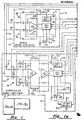
- FIG. 1 there is shown an atrial sense amplifier 10, ventricular sense amplifier 12, atrial output stage 14, ventricular output stage 16, digital control ana logic circuit 18, and three further circuits, the RF demodulator circuit 20 for receiving remotely applied programming signals and magnetic field test signals, a crystal oscillator 22 for providing the basic clock frequency for the digital control and logic circuit 18, and a voltage controlled oscillator (VCO) circuit 24 for timing certain operations of the digital control and logic circuit 18.
- the atrial sense amplifier 10 is coupled between tne atrial lead terminal 26 and tne case terminal 28 for sensing atrial depolarizations, or P waves.
- the ventricular sense amplifier 12 is similarly coupled to the case terminal 28 and the ventricular pacing lead terminal 30, for sensing ventricular aepolarizations, or R waves.
- the digital control and logic circuit 18 is coupled to the output terminals of the atrial and ventricular sense amplifiers to receive the atrial amplifier output signal at terminal 50 and the ventricular amplifier output signal at terminal 74, to process the signals in accordance with the mode to which the pacemaker is programmed and the parameters of atrial and ventricular timing escape intervals and to produce, if appropriate, atrial pace initiate signals PWA and ventricular pace initiate signals PWV.which are respectively coupled to input terminals of the atrial output stage 14 and the ventricular output stage 16 to initiate respective atrial and ventricular stimulating pulses.
- the production of the atrial and/or ventricular initiate pulses is dependent upon the presence or aDsence of sensea atrial and/or ventricular depolarizations of the heart within certain escape intervals established by the parameter data stored in memory within the digital control and logic circuit 18 and dependent upon whether or not the reed switch 32 is open or closed by the application of an external magnet or on the condition of interference detector 34 within the ventricular sense amplifier 12 which responds to noise signals picked up by the ventricular sense amplifier.
- the pulse generator will pace at a programmable lower rate it neither P waves nor R waves are sensed within the escape intervals established by lower rate data stored in memory.
- the A-V interval between the production of atrial and ventricular initiate signals by the digital control and logic circuit 18 is similarly programmable and, under these conditions, the total operation of the pacemaker is characterized as A-V sequential, demand pacing.
- the digital control and logic circuit 18 will not produce an atrial pace initiate signal, but instead will commence the timing of the A-V interval. If an R wave is sensed by the ventricular sense amplifier 12 prior to the expiration of the A-V interval, the ventricular pacing initiate signal is similarly not produced, and all timing intervals will be reset. But if an R wave is not sensed prior to the completion of the A-V interval, a ventricular pace initiate pulse will be provided by the digital control and logic circuit to initiate the production of a ventricular pacing stimulus at the end of the delay.
- the digital control and logic circuit 18 responds only to R waves sensed by the ventricular amplifier 12 and produces only ventricular pace inititate signals in the absence of an R wave occuring prior to the expiration of tne ventricular escape interval.
- the atrial output signal of the atrial sense amplifier 10 is similarly ianored. However, the atrial output stage and the ventricular output stage receive atrial and ventricular pace inititate signals at the programmable lower rate and separated by the A-V interval. It an R wave is sensed during the escape interval and following the refractory period of the ventricular sense amplifier, the lower rate timing is reset. If an R wave is sensed prior to the completion of the A-V interval and following the delivery of an atrial stimulating pulse to the heart, then the ventricular pace initiate signal is inhibited or not delivered, and the lower rate escape interval is again reset.
- Atrial synchronous ventricular inhibited, or VDT/I mode P waves recurring at a rate exceeding the programmable lower rate, are sensed by the atrial sense amplifier and processed by the digital control and logic circuit 18 to commence the A-V timing interval. Again, if an R wave is sensed prior to the completion of the A-V interval, the ventricular pacing output is inhibited and all timing circuits will be reset. But, if an R wave is not sensed prior to the completion of the A-V interval, a ventricular pacing stimulus will be provided in response to a ventricular pace initiate signal at the end of the A-V interval. A sensed R wave occurring within the programmed lower rate escape interval and after the refractory period since the last ventricular depolarization or stimulating pulse, will be processed by the diaital control and logic circuit 18 to restart the lower rate timing interval.
- the above modes of operation may be selected by tne pnysician to contorm the operation of the pacemaker to the patient's condition or the condition of the atrial or ventricular pacing leads. Ordinarily it would be expected that the pacemaker would be left operating in the fully automatic dual chamber or DDD mode, with the lower rate interval, A-V timing interval and other parameters of operation of the device Doing selected and programmed to conform to the patient's condition.
- the atrial sense amplifier 10 is coupled to the atrial lead 26 and the pulse generator 28 through conductors 36 and 38, 40 respectively.
- the conductors 36 and 38 are coupled to the negative and positive input terminals of differential amplifier 42 to a balanced resistance and capacitive network circuit 44 and 46 connected between the input and output terminals of the differential amplifier 42.
- the differential output signal of the amplifier 42 is coupled to a reversion circuit 48 which is designed to detect natural heart depolarizations in the presence of continuous noise signals.
- the reversion circuit 48 responas to the amplified signal to produce a P wave output signal which is applied to the input terminal 50 of the digital control and logic circuit 18.
- Atrial sense amplifier 10 depicted in FIG. 1 also shows a pair of reversion capacitors 62, 64 and a trim resistor 66 coupled to the reversion circuit 48.
- the differential amplifier 42, the reversion circuit 48, the battery monitor 56 and gain control resistors 68 and 70 can be packaged within a linear circuit chip 71 coupled to source voltage Vcc and system ground.
- the atrial sense amplifier as described conforms substantially to that depicted and described in the aforementioned U.S. patent N° 4,266,551.
- the ventricular sense amplifier 12 is coupled by conductors 40 and 72 to the pulse generator case 28 and the ventricular lead 30, respectively, and at its output terminal 74 to the digital control and logic circuit 18.
- the ventricular sense amplifier contains a FET switch array 76, a first differential amplifier 78, a second differential amplifier 80, a reversion circuit 82, a secona battery monitor circuit 84, and various biasing and filtering components.
- the ventricular sense amplifier 12 is designed to detect ventricular depolarizations and to avoid detecting atrial stimulating pulses delivered by the atrial output stage 14.
- the ventricular sense amplifier 12 is provided with a FET switch array 76 and the first differential amplifier 78 coupled D etween the output terminals 28 and 30 and the input terminals of a second differential amplifier 80.
- the FET switch array 76 possesses a first pair of series switches of transmission gates controlled by a first switch signal SV1 at terminal 88 and a second switch signal SV2 at terminal 86.
- the transmission gates 90 and 92 are coupled in series with the positive ana negative input terminals of differential amplifier 78 and the transmission gates 94 and 96 are coupled in parallel with gain control resistors 98 and 100 coupled between the input and output terminals of amplifier 78. Orainarily, in the absence of signals SV1 and SV2, the gates 90 and 92 are closed and the gates 94 and 96 are open.
- the differential amplifier 78 is ordinarily coupled to series connected RC filter circuits 79, 77 and the conductor 72 and 40 to the ventricular lead 30 and pulse generator case 28 respectively, and the gain of the differential amplifier 78 is controlled by the value of the resistors 98 and 100.
- signals appearing on the conductors 40 and 72 are differentially amplified in the balance differential amplifier 78 and coupled to R C circuits 1U2 and 104 to the second differential amplifier 80.
- the output signals are coupled to a reversion circuit 82 to provide an R wave amplifier output signal at the terminal 74 of the digital control and logic circuit 18.
- the signals SV1 and SV2 are generated just prior (e.g. 2 clock pulses earlier) to the generation of an atrial pace initiate pulse PWA which is delivered to the atrial output stage 14.
- the signals SV1 and SV2 are applied to tne transmission gates 90-96 to open the gates 90 and 92 and close the gates 94 and 96 to disconnect the input terminal of the differential amplifier 78 from the conauctors 40 and 72 and lower tne amplifier's gain by shorting out the resistors 98 and 100.
- the signal SV1 ceases, thus restoring the connection of the differential amplifier 78 to tne conauctors 40 ana 72.
- the reversion circuit 82 also includes circuitry which upon receiving an appropriate programming signal from the digital control and logic circuit 18 can adjust the sensitivity of the ventricular sense amplifier 12 through a signal on terminal 106, and circuitry for responding to a further switch signal SV3 at terminal 108 for blanking the ventricular sense amplifier 12 following the sensing of an earlier ventricular depolarization or the production of a ventricular pace initiate signal.
- the ventricular sense amplifier 12 further comprises a second battery monitoring circuit 84 for producing a second end-of-life signal EOL2 at terminal 110 when source voltage Vcc falls below a further lower reference voltage Vref2 established by the monitoring circuit 84.
- the ventricular sense amplifier 12 possesses the first and second reversion circuit capacitors 114 and 116, sensitivity trimming resistors 118 and an interference detecting circuit 34 for producing a signal SWE at terminal 120 when interference causes the capacitor 116 of reversion circuit 82 to become charged to a certain level.
- the control signal SWE at terminal 120 indicates to the digital control and logic circuit 18 that interference is present and causes it to provide certain control signals to insure that the reversion circuit 82 does not itself falsely produce an R wave output pulse at terminal 74 on the resumption of applied interference signals following the connection of the differential amplifier 78 to terminals 28 and 30 in the manner described above.
- first and second differential amplifier 78 and 80, the reversion circuit 82, the battery monitor circuit 84 and certain of the resistances would be constructed in a linear IC circuit 122.
- Filter and bias circuit components 75, 77, 102, 104, 112, 118 are selected to provide the appropriate frequency response and specification as is well known in the art.
- the reed switch 32 is shown coupled between the input terminal 124 and battery voltage B+.
- the closure of the reed switch 32 applies battery voltage to the terminal 124 and additional control and logic circuit 18 responds thereto to perform certain functions to be described in greater detail later, and to the RF demodulator 20 for enabling the RF demodulator 20 to demodulate applied RF signals detected in the tank circuit 21 and produce RF data output signals at the terminal 126.
- crystal oscillator 22 for providing the principal or fast clock signal for counting operations of digital control and logic circuit 18.
- a VCO circuit 24 comprising a voltage controlled oscillator and its associated trimming components which provides the clock frequency for the output pulse widths is also shown in FIG. 1.
- the VCO circuit 24 upon receiving a VCO ENABLE signal at terminal 130, applies the VCO output signal to the terminal 132 of the digital control and logic circuit 18, the frequency of the VCO output signal being dependent on the then prevailing source voltage Vcc and the digital control and logic circuit 18 produces the VCO ENABLE signal at the terminal 130.
- the VCO circuit 24 responds and provides the VCO OUT signal at the terminal 132.
- the digital control and logic circuit 18 responds to tne VCO OUT signal to employ the VCO signal as a timing signal in timing tne widths of the atrial anc ventricular pace initiate signals, thereby effecting an increase in the width of the atrial and ventricular stimulating pulses from the width programmed in memory within the digital control and logic circuit 18.
- VCO circuit 24 and the digital control and logic circuit 18 for effecting this mode of operation of the device is described in the aforementioned U.S. Patent No. 4,230,120.
- the atrial and ventricular output stages 14 and 16 each comprise defibrillation protection diodes 142 and 144 and an output capacitor 134 and 136 respectively connected to the atrial lead terminal 26 and ventricular lead terminal 30.
- the output capacitors are charged to battery voltage B+ and are discharged through transistor switches (not shown) within the atrial output stage 150 and the ventricular output stage 152, respectively, and commonly through the conductor 154 and case terminal 28 through the hear tissue and back to the terminals 26 and 30, respectively.
- the ventricular output capacitor 136 is recharged through conduction of transistor 140 while tne stored output capacitor 134 is recharged through the transistors 138, 146, and capacitor 148 and in relation to tne voltage on reference capacitor 149.
- the recharge cycle is under the control of a fast recharge
- control signal FRV developed by the digital control and logic circuit 18 at terminal 156.
- Tne pulse widths of the atrial and ventricular stimulating pulses are established by the widths of the atrial and ventricular output initiate signals PWA and PWV at terminals 158 and 160 respectively.
- Tne atrial and ventricular output stages 150 and 152 are coupled between regulated supply voltage Vcc ana system, ground through respective biasing components 161 and 162 in a manner well known in the art.
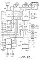
- FIG. 2 shows the circuit components for receiving externally applied programming signals for programming the modes and parameters of operation of the digitally controlled pacemaker of FIG. 1, memory storage for storing the programming signals, various counting circuits for timing the lower rate escape interval, the upper rate maximum allowed pacing rate, the A-V time delay, and other intervals for setting the pulse width duration of the atrial and ventricular output initiate signals and atrial and ventricular sense amplfiier sensitivities, and switching circuitry for controlling the modes of operation of the pacemaker.
- the circuit of FIG. 2 is implemented in digital logic components and circuits of said type shown in the aforementioned U.S. Patent No. 4,230,120. Distinctions arise from the fact that the circuit disclosed in that application is intended for control of a ventricular demand or VVI mode pacemaker, and the present invention is implemented in the context of a programmable, fully automatic dual chamber pacemaker normally operable in the DDD mode.
- the 32 kHz crystal oscillator trequency is applied at terminal 128 to a frequency divider circuit 200 which produces a 512 Hz slow clock signal at terminal 202 and a 4 kHz decoain g signal at terminal 204.
- the 4 kHz signal is applied to the program pulse aecoder 210 which decodes incoming RF signals appearing at terminal 126 to separate logic 1 and logic 0 signals from one another.
- the program pulse decoder 210 applies the decoded aata signals to the D input terminal of the shift register 212 and a clocking signal to the C input terminal of tne shift register 212.
- the shift register 212 accumulates the aecoded data signals and performs parity checking to assure that the serially received incoming data signals comprise properly formed programming words.
- the decoded data signal at terminal D of shift register 212 is a series of 33 pulse signals separatea by short and long intervals defining 32 logic 1 or logic 0 data bits.
- the 32 bit aata woras consists of four parts, each of which is 8 bits in length. The four parts are the parameter code, date or value coae, access code and parity code and are generated in that order, the least significant bit first.
- the parameter portion of the data signal defines one of several parameters (including modes of operation) to be modified and whether that modification is to be in a temporary or permanent matter, if that choice is available.
- the several parameters include "mode” comprising threshold check mode, the fully inhibited mode, the DDD mode, the DVI mode, the VDT/I mode, the VVI mode, the sensitivities of the sense amplifiers, the A-V period, the lower pacing rate, and the upper pacing rate, the atrial and ventricular stimulation pulse widths.
- mode comprising threshold check mode, the fully inhibited mode, the DDD mode, the DVI mode, the VDT/I mode, the VVI mode, the sensitivities of the sense amplifiers, the A-V period, the lower pacing rate, and the upper pacing rate, the atrial and ventricular stimulation pulse widths.
- the inhibit and threshold check parameters can only be done in a temporary mode whereas all the others can either be permanently or temporarily programmed.
- the programming parameter code and value codes are similar to but not necessarily the same as those set forth in the aforementioned U.S. Patent No. 4,230,120, and in any event can be arbitrarily selected by those skilled in the art.
- Tne shift register 212 contains eight access code storing stages, access aecoding and parity bit checking logic circuitry for insuring that the access code is correct and that the program word possesses proper parity, five parameter code shift register states for storing the five most significant bits of the eight bit parameter code (the first three bits of the eight bit parameter code are not used whatsoever and are always generated as logic 0 bits), and eight data or value code storage shift register stages for storing eight bits which define a particular value for the parameter selected.
- Ten further storage register stages and logic circuitry coupled parameters and data storage stages and certain stages of memory 214 effect the transfer of the parameters, e.g., the mode, lower rate, A-V interval, upper rate, atrial pulse width, ventricular pulse width, temporary atrial and ventricular pulse width and atrial and ventricular sense amplifier sensitivities.
- the parameters e.g., the mode, lower rate, A-V interval, upper rate, atrial pulse width, ventricular pulse width, temporary atrial and ventricular pulse width and atrial and ventricular sense amplifier sensitivities.
- a "master" portion of each word is accepted in memory 214 when the access code and parity check are found valid and all 32 bits of the program word is received. Further program transfer logic circuitry within the shift register 212 affects the shifting of the parameter data from the shift register 212 to the "master" register of the memory 214 in the permanent or temporary programming modes described here l n D etore. On acceptance of the transferred word, the shift register stages of shift reqister 212 are verified to accept the subsequently applied programming signal.
- all parameters and parameter values are stored within the memory 214, except that (1) if the parameter is "mode” and the value is “inhibit”, then the word is not transferred but is applied to the circuit to inhibit all operations; and (2) if the parameter is "sensitivity” and the value code contains the indicator "new value”, then only tne word can be transferred.
- the memory 214 contains address decode logic circuitry, master memory register 215 and slave memory register 217.
- Each decoded programming word from shift register 212 is transferrea into tne master register 215. Transfer of all contents of the master register 215 into the slave register 217 occurs only when the last word, indicated by a particular parameter code, has been stored in master portion 215, all the stored words possessed the valid access code and satisfied the parity check, and a ventricular pacing output pulse occurs after the last word and before receipt of any further words.
- the master and slave registers also perform the function of temporary and permanent memory in the manner described in the atorementioned U.S. Patent No. 4,230,120 for storing the various parameters and parameter values previously described and effecting the operation of the digital control and logic circuit 18 accordingly.
- Separate memory stages are devoted to the sensitivity of atrial and ventricular sense amplifiers, the programmable upper rates, the programmable lower rate or basic escape interval, the atrial and ventricular stimulation pulse widths, the A- V delay intervals, and data signifying the mode of operation of the device from among the various modes previously mentioned.
- the memory 214 furthermore possesses a hard wired lower rate for VVI mode that constitutes a basic safety rate should the power source energy momentarily dip below the circuits minimum operating requirements and also for use as one of the end-of-life test rates.
- the pulse generator will operate in a VVI mode at a preaetermined rate, for example, 65 beat per minute, and at a predetermined pulse width if either condition exists.
- the EOL2 signal is applied at terminal 110 to the memory 214 and, under certain circumstances of operation to be described, its presence causes the hard wired safety rate to be substituted for the programmed rate upon magnet mode testing of the battery aepletion.
- Tne lower rate aata is transferred by bus line from the memory 214 to the R-R or lower rate counter 216.
- Tne A-V interval data is transferred by Bus to the P-R counter 218 ana to the R-R counter 216.
- the upper rate data is transferred from the memory 214 to the upper rate circuit 220.
- the pulse width data, PDA and PDV for the control of the atrial and ventricular pulse widths is applied by bus lines from tne memory 214 to the pulse width control circuit 224.
- the upper rate counter 220 is coupled by a bus line to the PV C acceptance circuit 226.
- the R-R interval counter 216 comprises a ten stage shift register counter at least eight stages of which are coupled through decoding logic circuitry to the memory stages of the memory 214 which specify the programmed lower rate values and the A-V values.
- the R-R counter stages constitute therefore a presettable down counter, which is downcounted under the control of the 512 Hz slow clock frequency or under the control of a magnet actuated clock frequency of approximately 551 Hz when the safety margin indicator (SMI) counter 230 is activated by the reed switch closure.
- the SMI counter 230 alters the number of stages of divider 200 to change the slow clock frequency to 551 Hz until it counts three VPT outputs of the R- R counter.
- the clock frequencies downcount the loaded counter until a first count is reached which, when decoded, provides an atrial pulse trigger signal APT and until a subsequent second count is recorded which, when decoded, provides a ventricular pulse trigger signal VPT.
- APT and VPT are applied to the P-R counter 218 and the mode switch 222.
- the pacing rate is increased by 10 percent to indicate closure of tne reed switch.
- the SMI operation is therefore similar to that described in greater detail in the aforementioned U.S. Patent No. 4,230,120.
- the P-R counter 218 is an up counter that counts the 512 Hz slow clock signal from zero to the by A-V data count in memory 214. Upcounting commences when the signal PSV is received from moae swith 222 or the signal APT is received by the PR counter 218 and ceases when the count reaches a preselected number or the counters are reset by a sensed R wave.
- the mode switch 222 also receives the signal APT and VPT ana the moae data signals on a bus line from memory 214.
- the mode signal data sets the logic and switching circuits in the mode switch 222 to the modes previously described.
- the mode switch 222 responds to the signals APT and VPT to produce the P pace and R pace signals that are applied to the pulse duration counter 224.
- the pulse duration counter 224 responds to the P pace signal ana the atrial pulse duration data signal PD A to produce the atrial output initiate signal PWA at terminal 158 and similarly responds to the R pace signal at the ventricular pulse duration data signal DDD to produce the ventricular output initiate signal PWV at the terminal 160.
- the mode switch 222 also provides signals PSE and RSE that enable or disable the atrial and ventricular sense amplifiers 10 and 12.
- the output initiate signals PWA and PWV may possess durations that deviate from the programmed pulse duration signals. This can occur when the battery or power source depletes in energy.
- the VCO 24 (FIG. 1) automatically changes its frequency with the source voltage, that is, it decreases as the voltage decreases.
- the VCO output signal at terminal 132 (FIG. 1) is coupled to the PD counter 224 (FIG. 2) and provides its clock signal.
- the frequency slows, the time interval necessary to achieve the PDA or PDV count increases, thereby widening the output initiate pulses PWA ana PWV. This operation is again like that described in the aforementioned U.S. Patent No. 4,230,120.
- the PVC acceptance circuit 226 responds to premature ventricular contractions sensed within the ventricular escape interval of the R-R counter to provide an output signal to reset the R-R counter timing.
- the circuit 226 also responds to the atrial and ventricular pacing events (P pace and R pace) developed by the mode switch 222 and the atrial and ventricular sense signals PSV and RSV to provide the ventricular sense amplifier 12 refractory period.
- the refractory period is decoded by the circuit 226 from the count on the upper rate counter 220, and is ordinarily 233 ms after a paced or sensed ventricular event. But, if a PVC is sensed and triggers circuit 226, tnen the upper rate counter count is decoded to provide a 342 ms refractory period.
- the circuit 226 further establishes a 342 ms A-V delay interval commenced on the subsequently sensed atrial depolarization. This prolongation is employed to prevent a ventricular output pulse triggered by a sensed P-wave from possibly falling within the heart's vulnerable zone following the preceding premature ventricular contraction. This operation is further described in my commonly assigned copendina U.S. Patent Application Serial N° 235,232,filed 17 February, 198 1 .
- the A-V counter is also disabled for 342 ms (bigeminy A-V disable).
- the device is programmed to VVI or DVI moae, ventricular amplifier outputs after ventricular blanking and before refractory ends cause another 125 ms ventricular blanking timer and the ventricular refractory period to be set again to 233 ms.
- the digital reversion window will be equal to 108 ms.
- This pacemaker as described hereinbefore has sense amplifiers 10, 12 and pulse output circuits 14, 16 for connection to both the ventricle and atrium.
- Two unipolar electrodes are coupled to terminals 26 and 30 and the can 28 of tne pulse generator serves as a common indifferent electrode.
- Tne device can be programmed to operate in the DDD, DVI, VDT/I and VVI mode, but may have numerous resultant modes depending on the programming of the output pulse widths and amplifier sensitivities and on the natural underlying heart rhythm.
- Such resultant modes can include DAT/I, DVI, DOO, AOO, VOO, VAT, AVI, AAI, ADT/I and 000.
- the programmable lower rate establishes tne rate at which the pulse generator will pace if no P or R waves are sensed. At this rate the operation is A-V sequential and the interval between atrial and ventricular outputs (the A-V interval) is programmable.
- a P-wave If a P-wave is sensed, it will inhibit an atrial pacing output and trigger the A-V interval circuitry. If an R-wave is sensed prior to the completion or the A-V interval, the ventricular pacing output is inhibited and all timing circuits will be reset. If an R-wave is not sensed prior to the completion of the A-V interval, a ventricular pacing output will occur at the end of the delay.
- the atrial amplifier After an atrial event (sensed P-wave or atrial pacing output) the atrial amplifier is blanked.
- the ventricular amplifier 12 is also blanked for 15, 6 ms (ventricular blanking) after an atrial output to avoid sensing the voltage induced on the ventricular lead.
- the atrial amplifier 10 remains off until after the next ventricular event and is turned on only after the ventricular amplifier 12 has been on for 31 ms. This is to help insure that when both amplifiers are D eing turned back on that possible ectopic events which may occur are sensed first by the ventricular amplifier or are not sensed at all. If both amplifiers are turned on simultaneously, there exists the possibility that a heat depolarization could have just passesa by the ventricular electrode and will not be sensea by that amplifier.
- tnat same event could reach the atrial electrodes later and be regarded as a P-wave starting tne A-V interval and causing a ventricular stimulating pulse.
- Such ectopic events that occur high in the ventricle are likely to be sensed in the atrium.
- the consequence of the PVC sensed as a P-wave could be to pace one A-V interval later into what may be the repolarization phase of the PVC if the PVC is not sensed by the ventricular sense amplifier.
- the atrial blanking overlap is described in greater detail in commonly assigned, co-pending U.S. Patent Application Serial No. 145,052, filed April 30, 1980, by Harold Toby Markowitz.
- a P-wave sensed after the atrial amplifier 10 is turned on out before the end of the upper rate period will trigger an A-V interval by the P-R counter 218; however, the pulse gnerator will wait until the end of the upper rate period before a ventricular output will occur. This implements the upper rate characteristic of the atrial triggering mechanism.
- the upper rate period is started by the upper rate timer/counter 220 (at rates of 100, 125, 150, or 175 bpm) and the 233 ms ventricular refractory is started.
- the lower rate timer 216 cannot be reset. The timer 216 will be reset by either a ventricular pacing output or sensed R-wave which occurs outside of the ventricular refractory period.
- a ventricular sense amplifier output will restart the 233 ms refractory period, 125 ms R-blanking, 156 ms atrial blanking and upper rate period.
- the ventricular amplifier outputs after ventricular blanking and before refractory ends cause anotner 125 ms ventricular blanking, 156 ms atrial blanking and the ventricular refractory timer to be set to 342 ms (PVC refractory) provided that no prelettinging P-wave has been sensed.
- PVC refractory 342 ms
- there is a window of 342-125 217 ms for a retriqgering of refractory.
- the ventricular amplifier outputs must be no further apart than 342 ms.
- the pacemaker will operate A-V sequential asynchronous (DOO) because the lower rate timer will not be reset from ventricular amplifier outputs. This corresponds to a lowest interference frequency of 2.9 Hz.
- the R-refractory timer will be set to 233 ms as described hereinbefore.
- Tne pacemaker programmed in the DDD mode will perform in a pseudo-wenckebach fashion when atrial rates exceed the programmed upper rate. There will be gradual A-V lengthening until an atrial beat does not lead to a ventricular pacing output. The process then repeats. At high upper rates the device will reach 2:1 block dependent upon the programmed A-V interval.
- TABLE 1 depicts a table of the modes of operation and the rates that the pulse generator exhibits in response to the closure of the reed switch 32 and the presence of none, one or both of the signals EOL1 and EOL2 and
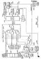
- FIG. 3 depicts in block diagram form a preferred circuit for achieving the modes and rates of TABLE 1.
- the battery power source is of the type which decreases in voltage over time, from an initial voltage of 2.8 volts, for example.
- the battery monitors 56 and 84 are operable to detect the depletions below 2.2 volts and 2.0 volts, respectively for example, to provide the EOL1 and EOL2 signals at terminals 60 and 110.
- the magnet signal at teminal 124 ana the EOL1 signal at terminal 60 are coupled to the R-R or lower rate counter 216 and the EOL2 signal at terminal 110 is coupled to the memory 214.
- the pacemaker responds to the closure of the reed switcn 32 in a manner similar to the response described in the commonly assigned, co-pending U.S. Patent No. 4,230,120. Briefly, the closure of the reed switch causes the pulse generator to operate in an asynchronous mode wherein the sense amplifier output signals are ignored and at a rate different than the programmed rate. The third synchronous atrial ana ventricular output pulses are reduced in width to 75 percent of their programmed (or pulse width stretched) pulse widths.
- One observing the EKG can thus ascertain that the reed switch is closed so programming or telemetry can commence and the capture or noncapture of the third pulses sequence provides a safety margin indicator (SMI as earlier described).
- SI safety margin indicator
- the resultant modes and rate of pacing demonstrate both the programmed mode and the battery depletion level.
- the four normally programmed modes in the leftmost column change on application of the magnet to DOO for the modes DOO, DVI and to VOO for the modes VVI, VDT/I at beginning of life (BOL) and at EOL1.
- the rates indicate the difference netween DDD and DVI and between VVI and VDT/I (AP on the chart indicting "as programmed").
- the rates of 85, 75 and 65 are selected since these are rates not contemplated to be programmable rates.
- the magnet mode end safety margin indicating rates of the present invention are plus 10 percent of the rates 85, 75, 65 or AP.
- the rates are 93.5, 82.5 or 71.5 bpm depending on the EOL condition.
- the rates are the preset test rates of 85, 75 and 65 b pm, respectively.
- the 10 percent rate change is effected by the 5MI counter 230 of FIG. 2 which commences counting output signals VPT of the R-R counter and until three pulses are counted disables a stage in the divider 200 to increase the clock frequency from 512 Hz to 551 Hz.
- the faster clock frequency when applied to P-R counter 218 and R-R counter 216 causes the 10 percent increase in the respective atrial and ventricular rates.
- the rate of 85 bpm or AP and the asynchronous modes DOO or VOO signify ncrmal conditions and allow the observer to determine the programmed mode.
- the EOL1 signal coupled to the R-R counter causes the R-R counter to ignore the programmed rate count by presetting the decoding logic between the lower rate data bus and the counter stages and thereby substituting the preset count (corresponaing to 75 or 82.5 bpm) for the rate data count in memory 214.
- the P-R counter decoding circuit is loaded with a preset count and one or both (depending on the DOO or VOO mode) counters 216 and 218 are incremented by the slow clock pulses to provide output pulse(s) at the 75 or 82.5 bpm rate.
- the rate is the same for all programmed modes. Therefore, it is only possible to distinguisn the dual and single chamber programmed modes.
- the EOL1 condition would, in any case, call for closer examination and monitoring of the device because it indicates imminent battery depletion. The observing physician would schedule a procedure to remove and replace the device or prolong its life by changing to a simpler mode, e.g. VVI, or lowering the pacing rate.
- the application of the magnet causes the SMI sequence as earlier described and then operates the pulse generator in the VOO Mode regardless of the programmed mode and at a rate of 65 bpm. This indicates to the observing physician that final battery depletion is near and that the unit is to be replaced.
- the 65 bpm rate is accomplished at magnet application by operation of logic circuitry within the memory 214 wnich responds to the EOL2 signal on terminal 110 and advantageously loads in tne safety rate of 65 bpm which is hardwired into memory 214.
- the safety rate thus is directed on L-R data bus line to R-R counter 216 to control the rate in the VOO mode in precedence over the pro g rammea rate.
- the pulse generator in this condition does not return to the programmed mode or rate but remains at the 65 bpm rate in the VVI mode to aecrease the current demand in the power source.
- the safety rate ana mode take precedence over the programmed rate ana mode.
- the pulse generator can no longer be reprogrammed; however, it could oe designed to allow the physician to subsequently reprogram the pulse generator.
- the EOL2 mode and rate indicates to the observing physician that the pulse generator should be replaced as soon as practicable.
- FIG. 3 there is depicted a block diagram of a circuit for effecting the end-of-life test rates and modes described in reference to TABLE 1 and in the context of FIGs. 1 and 2.
- Tne circuit of FIG. 3 responds to the EOL1 signal at terminal 60, the EO L 2 signal at terminal 110, the closure of the reed switch at terminal 124, the clock input at terminal 128 and the contents of the mode and rate memory to provide the modes and rates hereinbefore mentioned.
- the rates are established by the eight stage counter 250 (in the R-R counter 216) which is loaded with selected rate data and downcounted by the 512/551 Hz clock 200 until a first count is obtained which is decoded by the P-R decoder 252 to produce the atrial pace trigger signal APT, and then downcounted to a further predetermined number whereupon the R-R decoder 254 produces the ventricular pace trigger signal VPT.
- the selected rate count is loaded into the counter 250 by the rate select logic 256 each time the counter 250 is triggerea by the trigger logic 258.
- the selected rate count is one of four possible counts, including the programmed count and tne 65 bpm safety rate, both present in the rate memory stages 258, the 75 bpm preset logic circuit 260, and the 85 bpm count of preset logic circuit 262.
- the selection of the one of the four possible rate counts is controlled by mode select circuit 220 and by the presence or absence of the EOL1 and EOL2 signals which set the respective EOL1 and EOL2 data registers 264 and 266.
- the closure of the reed switch 32 provides a signal at terminal 124 and sets the magnet enable register 268.
- the setting of the magnet enable recister 268 causes the SMI counter 230 to change the clock frequency of clock 200 from 512 Hz to 551 Hz for three R-R cycles of the eight stage counter 250 subsequent to the next following delivery of a ventricular pace triaaer VPT.
- the set state of the magnet enable register 268 is also conveyed to the mode select logic 270 and to the trigger logic 258.
- the mode select logic 270 receives a further input from the mode memory stages 272 of the memory 214 (FIG. 2).
- the moae select logic 270 is triggered by the set state of the magnet enable register 268 to provide an output signal which is applied to the P-R decoder 252 to, in certain instances be described, disable the decoder 252 thus preventing the production of an atrial pace trigger pulse APT.
- the trigger logic circuit 258 responds to the next occurring VPT signal for providing a trigger signal to the T input of counter 250.
- the mode data of the mode memory stages 272 is also applied to the P-R decoder 252 to disable the decoder 252 under EOL2 conditions.
- the registers 264 and 266 are not set.
- the programmed rate data that is in the rate memory stages 258 is applied to the rate select logic 256 to one input of AND gate 274.
- the 85 bpm preset logic 262 provides the 85 bpm preset rate to one input of AND gate 276 in the rate select logic 256.
- the rate select logic 256 selects the programmed rate and applies it to the counter 250.
- the rate select logic 256 is, in response to the trigger signal, preset to 85 bpm by the preset logic 262, and the 85 bpm rate count is loaded into the counter 250.
- the asynchronous pacing rate is either 85 bpm (93.5 bpm for the first three pacing intervals) or the programmed rate, aepending on the programmed mode. In either case, the data is loaded into counter 250 throuah OR gate 280.
- the selection of tne programmed rate or the 85 bpm rate is accomplished by the mode select 270, tne AND cate 282 and the inverter 264.
- the magnet enatle signal and the EOL1 signal are at high logic levels and are applied to inputs of AND gate 282. If the DDD or VDT/I modes are programmed in memory stage 272, then the output on line 286 of mode select 270 is also high and the output of AND gate 282 goes high.
- the high output is coupled to an input of AND gate 276 and that gate 276 is enabled to pass the 85 bpm count data througn OR gate 280 to the counter 250.
- the other two gates, 274 and 278 are disabled by the low logic level output of inverter 284.
- the output 286 is low, and gate 282 is disabled. Since the EOL1 signal and the output of inverter 284 are high, then the rate count for rate memory stage 258 is transmitted through AND gate 274 and OR gate 280 to load the counter 250.
- the AND gate 274 is therefore enabled, and tne gates 276, 278 and 282 are disabled.
- the AND gate 274 also, in the ordinary operation of the pulse generator, applies the programmed rate count to the counter 250.
- the EOL1 data register 264 is set causing the EOL1 signal to go high.
- the AND gate 278 is enabled and the AND gates 274 and 276 are disabled.
- the rate select logic 256 supplies the 75 bpm rate count under all programmed conditions to the counter 250.
- the data registers 266 and 264 are set ana reset, respectively. Simultaneously, the memory rate count is erased and the hardwired safety rate of 65 bpm is presented to the AND gate 274.
- the programmea mode is reset to the VVI mode so that the mode select 270 provides a signal on conductor 288 to disable the P-R decoder.
- the EOL1 signal is nigh and tne output of AND gate 282 is low, ana AND gate 274 is therefore enabled.
- the rate is therefore set at 65 bpm and the mode is set to the VOO mode at the time that the magnet is applied and to the VVI mode thereafter.
- the memory may contain hard wired safety or nominal values for other parameters, e.g. the ventricular pulse width (e.g. 0-5 ms), and the ventricular sensitivity (e.g. 2.5 mV).
- the nominal ventricular pulse width and sensitivity data are substituted for the programmed data and control operation of the pulse generator in the VVI mode at EOL2.
- the modes and rates related are arbitrary, but are selected to be distinguishable from normally programmable rates. It is contemplated that different rates could be related to distinguish each mode under each battery depletion condition. It is further contemplated that the end-of-life depletion circuits and modes herein described could as well be applied to pacemakers programmable in only two or more of the modes herein describea.
- the operating modes and parameters of any medical device other than a pacemaker pulse generator may similarly be changed to indicate its power source depletion level. The invention may thus find application in an implantable drug dispenser, nerve or tissue stimulator, blood pump or other medical device dependent on an depletable power source.
- the invention may also be implemented in any suitable analog or digital circuitry including software controlled custom or conventional microprocessors. These and other modifications or uses of the invention will be apparent to those skilled in the art.
Landscapes
- Health & Medical Sciences (AREA)
- Life Sciences & Earth Sciences (AREA)
- Veterinary Medicine (AREA)
- Animal Behavior & Ethology (AREA)
- Public Health (AREA)
- Engineering & Computer Science (AREA)
- Biomedical Technology (AREA)
- Nuclear Medicine, Radiotherapy & Molecular Imaging (AREA)
- Radiology & Medical Imaging (AREA)
- Heart & Thoracic Surgery (AREA)
- General Health & Medical Sciences (AREA)
- Cardiology (AREA)
- Biophysics (AREA)
- Physics & Mathematics (AREA)
- Acoustics & Sound (AREA)
- Electrotherapy Devices (AREA)
Applications Claiming Priority (2)
| Application Number | Priority Date | Filing Date | Title |
|---|---|---|---|
| US23506981A | 1981-02-17 | 1981-02-17 | |
| US235069 | 1988-08-22 |
Related Parent Applications (1)
| Application Number | Title | Priority Date | Filing Date |
|---|---|---|---|
| EP82400225.7 Division | 1982-02-09 |
Publications (3)
| Publication Number | Publication Date |
|---|---|
| EP0160801A2 true EP0160801A2 (fr) | 1985-11-13 |
| EP0160801A3 EP0160801A3 (en) | 1986-05-28 |
| EP0160801B1 EP0160801B1 (fr) | 1991-09-25 |
Family
ID=22883974
Family Applications (2)
| Application Number | Title | Priority Date | Filing Date |
|---|---|---|---|
| EP19820400225 Expired EP0058603B1 (fr) | 1981-02-17 | 1982-02-09 | Indicateur de l'état d'épuisement de la source d'alimentation de dispositifs médicaux implantables |
| EP19850102404 Expired EP0160801B1 (fr) | 1981-02-17 | 1982-02-09 | Indicateur de l'état d'épuisement de la source d'alimentation de dispositifs médicaux implantables |
Family Applications Before (1)
| Application Number | Title | Priority Date | Filing Date |
|---|---|---|---|
| EP19820400225 Expired EP0058603B1 (fr) | 1981-02-17 | 1982-02-09 | Indicateur de l'état d'épuisement de la source d'alimentation de dispositifs médicaux implantables |
Country Status (3)
| Country | Link |
|---|---|
| EP (2) | EP0058603B1 (fr) |
| AU (1) | AU547888B2 (fr) |
| DE (2) | DE3280360D1 (fr) |
Cited By (7)
| Publication number | Priority date | Publication date | Assignee | Title |
|---|---|---|---|---|
| WO1990009208A1 (fr) * | 1989-02-14 | 1990-08-23 | Siemens-Elema Ab | Dispositif electromedical implantable dans un corps vivant |
| US4966146A (en) * | 1988-01-14 | 1990-10-30 | Webb Stuart C | Rate-responsive pacemaker |
| EP0416138A1 (fr) * | 1989-08-28 | 1991-03-13 | Siemens-Elema AB | Appareil médical coopérant avec le corps d'un être vivant pour la stimulation et/ou la surveillance d'une fonction physiologique |
| US5044365A (en) * | 1988-02-17 | 1991-09-03 | Webb Stuart C | Rate-responsive pacemaker |
| EP0657186A3 (fr) * | 1993-12-09 | 1997-03-19 | Medtronic Inc | Stimulateur cardiaque dont les modes de fonctionnement sont commandés par un aimant. |
| US8942935B2 (en) | 2010-06-14 | 2015-01-27 | Medtronic, Inc. | Charge level measurement |
| US10204706B2 (en) | 2009-10-29 | 2019-02-12 | Medtronic, Inc. | User interface for optimizing energy management in a neurostimulation system |
Families Citing this family (6)
| Publication number | Priority date | Publication date | Assignee | Title |
|---|---|---|---|---|
| FR2504702A1 (fr) * | 1981-04-23 | 1982-10-29 | Ela Medical Sa | Procede de commande et de reglage notamment d'un stimulateur cardiaque, et dispositif pour sa mise en oeuvre |
| US4541431A (en) * | 1984-09-20 | 1985-09-17 | Telectronics Pty. Ltd. | Use of telemetry coil to replace magnetically activated reed switch in implantable devices |
| US5620474A (en) * | 1995-04-24 | 1997-04-15 | Vitatron Medical, B.V. | System and method for determining indicated pacemaker replacement time based upon battery impedance measurement |
| SE9904087D0 (sv) * | 1999-11-11 | 1999-11-11 | Pacesetter Ab | Recommended replacement time of an implantable medical device |
| US20060025828A1 (en) * | 2004-07-28 | 2006-02-02 | Armstrong Randolph K | Impedance measurement for an implantable device |
| US9795792B2 (en) | 2011-02-25 | 2017-10-24 | Medtronic, Inc. | Emergency mode switching for non-pacing modes |
Family Cites Families (9)
| Publication number | Priority date | Publication date | Assignee | Title |
|---|---|---|---|---|
| US3661158A (en) * | 1969-12-15 | 1972-05-09 | American Optical Corp | Atrio-ventricular demand pacer with atrial stimuli discrimination |
| DE2146965A1 (de) * | 1970-09-18 | 1972-05-25 | Devices Ltd | Implantierbarer Herzschrittmacher |
| US3756246A (en) * | 1971-07-15 | 1973-09-04 | American Optical Corp | Apparatus for externally determining actual output of an implanted energy source |
| US4120307A (en) * | 1976-10-26 | 1978-10-17 | Medtronic, Inc. | Cardiac pacemaker |
| US4095603A (en) * | 1976-12-17 | 1978-06-20 | Cordis Corporation | Cardiac pacer employing discrete frequency changes |
| US4190055A (en) * | 1977-07-05 | 1980-02-26 | Arco Medical Products Company | Circuit for determining the parameter control states of an implanted pacer |
| FR2427817A1 (fr) * | 1978-06-05 | 1980-01-04 | Roland Emballages | Procede et dispositif pour la surveillance de la force electromotrice d'une pile disposee dans le corps d'un etre vivant |
| IT1118131B (it) * | 1978-07-20 | 1986-02-24 | Medtronic Inc | Perfezionamento nei pacemaker cardiaci multi-modo adattabili impiantabili |
| AU530108B2 (en) * | 1978-11-06 | 1983-06-30 | Medtronic, Inc. | Digital cardiac pacemaker |
-
1982
- 1982-02-09 DE DE8585102404T patent/DE3280360D1/de not_active Expired - Lifetime
- 1982-02-09 EP EP19820400225 patent/EP0058603B1/fr not_active Expired
- 1982-02-09 DE DE8282400225T patent/DE3270708D1/de not_active Expired
- 1982-02-09 EP EP19850102404 patent/EP0160801B1/fr not_active Expired
- 1982-02-16 AU AU80509/82A patent/AU547888B2/en not_active Ceased
Cited By (10)
| Publication number | Priority date | Publication date | Assignee | Title |
|---|---|---|---|---|
| US4966146A (en) * | 1988-01-14 | 1990-10-30 | Webb Stuart C | Rate-responsive pacemaker |
| US5044365A (en) * | 1988-02-17 | 1991-09-03 | Webb Stuart C | Rate-responsive pacemaker |
| US5063927A (en) * | 1988-02-17 | 1991-11-12 | Webb Stuart C | Rate-responsive pacemaker |
| WO1990009208A1 (fr) * | 1989-02-14 | 1990-08-23 | Siemens-Elema Ab | Dispositif electromedical implantable dans un corps vivant |
| US5193538A (en) * | 1989-02-14 | 1993-03-16 | Siemens Aktiengesellschaft | In vivo implantable medical device with battery monitoring circuitry |
| EP0416138A1 (fr) * | 1989-08-28 | 1991-03-13 | Siemens-Elema AB | Appareil médical coopérant avec le corps d'un être vivant pour la stimulation et/ou la surveillance d'une fonction physiologique |
| US5159926A (en) * | 1989-08-28 | 1992-11-03 | Siemens Aktiengesellschaft | Medical stimulation and/or monitoring device interacting with the body of a patient based upon selectable parameter set |
| EP0657186A3 (fr) * | 1993-12-09 | 1997-03-19 | Medtronic Inc | Stimulateur cardiaque dont les modes de fonctionnement sont commandés par un aimant. |
| US10204706B2 (en) | 2009-10-29 | 2019-02-12 | Medtronic, Inc. | User interface for optimizing energy management in a neurostimulation system |
| US8942935B2 (en) | 2010-06-14 | 2015-01-27 | Medtronic, Inc. | Charge level measurement |
Also Published As
| Publication number | Publication date |
|---|---|
| DE3270708D1 (en) | 1986-05-28 |
| EP0058603A1 (fr) | 1982-08-25 |
| EP0160801B1 (fr) | 1991-09-25 |
| AU8050982A (en) | 1982-08-26 |
| EP0160801A3 (en) | 1986-05-28 |
| DE3280360D1 (de) | 1991-10-31 |
| EP0058603B1 (fr) | 1986-04-23 |
| AU547888B2 (en) | 1985-11-07 |
Similar Documents
| Publication | Publication Date | Title |
|---|---|---|
| US4390020A (en) | Implantable medical device and power source depletion control therefor | |
| US4606349A (en) | Implantable cardiac pacer having dual frequency programming and bipolar/unipolar lead programmability | |
| EP0058606B1 (fr) | Stimulateur atrial et ventriculaire | |
| US5441525A (en) | Pacemaker with vasovagal syncope detection | |
| US6400988B1 (en) | Implantable cardiac device having precision RRT indication | |
| AU616374B2 (en) | Atrial rate based programmable pacemaker with automatic mode switching means | |
| US5540728A (en) | Pacemaker with vasovagal snycope detection | |
| US5676686A (en) | Pacemaker with vasovagal syncope detection | |
| US5501701A (en) | Pacemaker with vasovagal syncope detection and therapy | |
| US7031773B1 (en) | Implantable cardiac stimulation system providing autocapture and lead impedance assessment and method | |
| AU654641B2 (en) | Implantable pacemaker providing hysteresis in dual-chamber modes | |
| US5800472A (en) | Recommended replacement time trigger for use within an implantable rate-responsive pacemaker | |
| EP0236562A1 (fr) | Appareil pour stimulation cardiaque avec détection des potentiels cardiaques provoqués | |
| EP0431437B1 (fr) | Système et méthode pour maintenir l'amplitude des impulsions de stimulation par auto-régulation de la consommation de courant lorsque la charge de la batterie s'épuise | |
| US4561444A (en) | Implantable cardiac pacer having dual frequency programming and bipolar/linipolar lead programmability | |
| EP0058603B1 (fr) | Indicateur de l'état d'épuisement de la source d'alimentation de dispositifs médicaux implantables | |
| CA2515771A1 (fr) | Mesure d'impedance dans un dispositif implante | |
| EP1879653B1 (fr) | Systeme de gestion de la saisie | |
| EP0757577B1 (fr) | Stimulateur cardiaque a detection de syncope vaso-vagale | |
| US7260433B1 (en) | Subcutaneous cardiac stimulation device providing anti-tachycardia pacing therapy and method | |
| US7027865B2 (en) | Pacemaker with vasovagal syncope detection and therapy | |
| US7606618B1 (en) | Implantable medical device with notification system | |
| US7035687B1 (en) | Implantable cardiac stimulation system providing capture threshold stability assessment and method | |
| US7756570B1 (en) | Methods and arrangements for reducing oversensing and/or providing diagnostic information in implantable medical devices | |
| US6694179B1 (en) | Display for and method of displaying electrograms received from an implantable cardiac stimulation device |
Legal Events
| Date | Code | Title | Description |
|---|---|---|---|
| PUAI | Public reference made under article 153(3) epc to a published international application that has entered the european phase |
Free format text: ORIGINAL CODE: 0009012 |
|
| 17P | Request for examination filed |
Effective date: 19850320 |
|
| AC | Divisional application: reference to earlier application |
Ref document number: 58603 Country of ref document: EP |
|
| AK | Designated contracting states |
Designated state(s): DE FR IT NL SE |
|
| PUAL | Search report despatched |
Free format text: ORIGINAL CODE: 0009013 |
|
| AK | Designated contracting states |
Kind code of ref document: A3 Designated state(s): DE FR IT NL SE |
|
| 17Q | First examination report despatched |
Effective date: 19871217 |
|
| GRAA | (expected) grant |
Free format text: ORIGINAL CODE: 0009210 |
|
| AC | Divisional application: reference to earlier application |
Ref document number: 58603 Country of ref document: EP |
|
| AK | Designated contracting states |
Kind code of ref document: B1 Designated state(s): DE FR IT NL SE |
|
| ITF | It: translation for a ep patent filed | ||
| REF | Corresponds to: |
Ref document number: 3280360 Country of ref document: DE Date of ref document: 19911031 |
|
| ET | Fr: translation filed | ||
| PLBI | Opposition filed |
Free format text: ORIGINAL CODE: 0009260 |
|
| 26 | Opposition filed |
Opponent name: BIOTRONIK MESS- UND THERAPIEGERAETE GMBH & CO ING Effective date: 19920625 |
|
| NLR1 | Nl: opposition has been filed with the epo |
Opponent name: BIOTRONIK MESS- UND THERAPIEGERAETE GMBH & CO |
|
| PGFP | Annual fee paid to national office [announced via postgrant information from national office to epo] |
Ref country code: FR Payment date: 19950113 Year of fee payment: 14 |
|
| PGFP | Annual fee paid to national office [announced via postgrant information from national office to epo] |
Ref country code: SE Payment date: 19950116 Year of fee payment: 14 |
|
| PGFP | Annual fee paid to national office [announced via postgrant information from national office to epo] |
Ref country code: DE Payment date: 19950123 Year of fee payment: 14 |
|
| EAL | Se: european patent in force in sweden |
Ref document number: 85102404.2 |
|
| PGFP | Annual fee paid to national office [announced via postgrant information from national office to epo] |
Ref country code: NL Payment date: 19950228 Year of fee payment: 14 |
|
| RDAG | Patent revoked |
Free format text: ORIGINAL CODE: 0009271 |
|
| STAA | Information on the status of an ep patent application or granted ep patent |
Free format text: STATUS: PATENT REVOKED |
|
| 27W | Patent revoked |
Effective date: 19950308 |
|
| NLR2 | Nl: decision of opposition | ||
| APAH | Appeal reference modified |
Free format text: ORIGINAL CODE: EPIDOSCREFNO |