EP0160941A2 - Hochspannungsverbindungssystem für eine integrierte Halbleiterschaltung - Google Patents
Hochspannungsverbindungssystem für eine integrierte Halbleiterschaltung Download PDFInfo
- Publication number
- EP0160941A2 EP0160941A2 EP85105376A EP85105376A EP0160941A2 EP 0160941 A2 EP0160941 A2 EP 0160941A2 EP 85105376 A EP85105376 A EP 85105376A EP 85105376 A EP85105376 A EP 85105376A EP 0160941 A2 EP0160941 A2 EP 0160941A2
- Authority
- EP
- European Patent Office
- Prior art keywords
- high voltage
- region
- voltage
- integrated circuit
- referenced
- Prior art date
- Legal status (The legal status is an assumption and is not a legal conclusion. Google has not performed a legal analysis and makes no representation as to the accuracy of the status listed.)
- Withdrawn
Links
Images
Classifications
-
- H—ELECTRICITY
- H10—SEMICONDUCTOR DEVICES; ELECTRIC SOLID-STATE DEVICES NOT OTHERWISE PROVIDED FOR
- H10W—GENERIC PACKAGES, INTERCONNECTIONS, CONNECTORS OR OTHER CONSTRUCTIONAL DETAILS OF DEVICES COVERED BY CLASS H10
- H10W20/00—Interconnections in chips, wafers or substrates
- H10W20/40—Interconnections external to wafers or substrates, e.g. back-end-of-line [BEOL] metallisations or vias connecting to gate electrodes
-
- H—ELECTRICITY
- H10—SEMICONDUCTOR DEVICES; ELECTRIC SOLID-STATE DEVICES NOT OTHERWISE PROVIDED FOR
- H10W—GENERIC PACKAGES, INTERCONNECTIONS, CONNECTORS OR OTHER CONSTRUCTIONAL DETAILS OF DEVICES COVERED BY CLASS H10
- H10W42/00—Arrangements for protection of devices
Definitions
- the present invention relates to high voltage interconnects (i.e., electrodes) utilized in a semiconductor integrated circuit for electrically interconnecting different devices in the integrated circuit.
- the invention more particularly relates to a high voltage interconnect system wherein high voltage interconnects are situated in close proximity to either highly-doped voltage-referenced regions or to lateral field-supporting regions.
- Semiconductor integrated circuits frequently include highly-doped voltage-referenced regions, that is, highly-doped semiconductor regions referenced to a known potential in the integrated circuit, as opposed to being unreferenced, or free floating, in potential.
- highly-doped is meant herein at least 10 17 , and, preferably, more than 10 20 , dopant atoms per cubic centimeter.
- high voltage as used herein constituting a voltage in excess of about 50 volts.
- the problem is that, unless adequate dielectric separation is provided between the voltage-referenced region and the high voltage interconnect, an extremely high electric field gradient may be created in the voltage-referenced region and causes device failure due to avalanche breakdown.
- An approach used in the prior art to assure adequate dielectric separation is to space the interconnect from the voltage-referenced region by a relatively thick, typically, 10 micron, insulation layer of silicon dioxide or silicon nitride. Such layers, however, are about 10 times thicker than other insulation layers typically provided on the integrated circuit device.
- the interconnect having a portion connected to the semiconductor surface, must scale the height of the thick insulation. It is difficult to assure that the vertical portions of the interconnect which scale the thick insulation are formed intact. Accordingly, device fabrication cost is increased since yields of operative devices are lowered.
- Integrated circuits frequently also include lateral field-supporting regions. These regions are used, for example, between a semiconductor device included in an integrated circuit and operated at high voltage and a grounded isolation region that surrounds the semiconductor device to isolate the semiconductor device from other devices contained in the integrated circuit.
- the influence of a high electric field, radiating from a high voltage interconnect and impinging upon the lateral field-supporting region can reduce the voltage that can be supported by the region.
- a prior art approach to preventing a high electric field from impinging on the field-supporting region is to dielectrically separate the overlying interconnect from the lateral field-supporting region by a thick insulator, such as a 10-micron layer of silicon dioxide or silicon nitride.
- a thick insulator such as a 10-micron layer of silicon dioxide or silicon nitride.
- the deleterious interference of high electric fields, radiating from a high voltage interconnect, upon a lateral field-supporting region is particularly acute where the voltage-supporting region has been designed in accordance with a technology known as reduced surface field (RESURF) technology.
- RESURF reduced surface field
- the product of the doping concentration and thickness of a lateral field-supporting region is typically in the range of about 0.2 x 10 12 atoms/cm 2 to 1.4 x 10 12 at oms/cm '.
- RESURF High Voltage Thin Layer Devices
- a further object of the invention is to provide a high voltage interconnect system for an integrated circuit that can be readily incorporated into existing high voltage integrated circuit fabrication processes.
- a high voltage interconnect system for an integrated circuit includes a semiconductor wafer having field-shield layers thereon.
- Each field-shield layer comprises a polycrystalline, oxygen-doped, silicon layer overlying a select region of the wafer and an insulating layer, such as silicon dioxide, overlying the polycrystalline, oxygen-doped, silicon layer.
- An interconnect electrode overlies the insulating layer and is adapted to operate at a potential difference of about 50 volts from that of the select region of the semiconductor wafer.
- the select region of the semiconductor wafer overlain by the interconnect comprises a voltage-referenced region doped in excess of about 10 20 dopant atoms per cubic centimeter. In another embodiment of the invention, the select region of the semiconductor wafer comprises a lateral field-supporting region.
- the combined thickness of the polycrystalline, oxygen-doped silicon layer and the insulating layer overlying such polycrystalline layer can be below about 1.3 microns, with attainment of successful shielding of the voltage-referenced region from high electric fields.
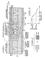
- Figure 1 illustrates an integrated circuit (IC), generally designated 10, incorporating features of the present invention.
- IC 10 includes a semiconductor wafer 20 containing an NPN bipolar transistor 12 in which current flow is vertical.
- Transistor 12 made up of base region 38, emitter region 40 and collector regions 36 and 42, includes a high voltage base interconnect 13 and a high voltage collector interconnect 15.
- Transistor 12 additionally includes an emitter electrode 17.
- IC 10 further includes a P (or high resistivity, P-conductivity type) substrate 18, which constitutes a common substrate for all integrated devices in IC 10, such as transistor 12.
- An electrode 19 adjoins P substrate 18 and is typically biased to a ground or reference potential.
- High voltage base interconnect 13 is spaced from semiconductor wafer 20 by field-shield layers 22 and 24.
- Layer 22 comprises a polycrystalline silicon layer that is doped with oxygen to an average of preferably between 2 and 45 atomic percent, this material being known in the art as Semi-Insulating Polycrystalline Oxygen Doped Silicon (SIPOS).
- SIPOS Semi-Insulating Polycrystalline Oxygen Doped Silicon
- oxygen doping of polysilicon can be accomplished by using low pressure, chemical vapor deposition technique to react silane and nitrous oxide at approximately 620°C to form polycrystalline silicon layer 22. Further details of preparation of suitable polycrystalline, oxygen-doped silicon can be found, for example, in "High Reliability High Voltage Transistors by Use of the SIPOS Process", IEEE Transactions on Electron Devices, Vol. 23, No.
- Layer 24 comprises an insulating material such as silicon dioxide overlying first layer 22.
- high voltage collector interconnect 15 is spaced from semiconductor wafer 20 by field-shield layers 26 and 28, which suitably are essentially similar to layers 22 and 24, respectively, beneath interconnect 13.
- Emitter interconnect 17 is spaced from a portion of transistor base region 38 via insulating layers 30a and 30b of silicon dioxide, for example, which also passivate the portions of wafer 20 covered by layers 30a and 30b.
- Emitter interconnect 17 is also spaced from the high voltage collector regions 36 and 42 by field-shield layers 32 and 34, which preferably overlap at least a small portion of transistor base region 38 to conveniently assure coverage of . collector regions 36 and 42.
- Field-shield layers 32 and 34 suitably are essentially similar to field-shield layers 22 and 24, respectively, beneath interconnect 13.
- IC 10 includes an N + high voltage tub 36, which forms a closed region around N region 42 and which may be round or square as viewed from above, by way of example.
- N + tub 36 contains the following semiconductor regions of NPN bipolar transistor 12: P base region 38, N + emitter region 40, and N collector region 42 (the superscripts "+” and "-” signifying low and high resistivity regions, respectively).
- N high voltage tub 36 is highly doped so as to provide a low resistance interconnection between N collector region 42 and high voltage collector interconnect 15. Further details of transistor 12 can be found by referring to copending, commonly-assigned application Serial No. 558,405, filed on 5 December 1983 and entitled SEMICONDUCTOR WAFER WITH AN ELECTRICALLY-ISOLATED SEMICONDUCTOR DEVICE, by EJ Wildi and TP Chow.
- IC 10 includes voltage-referenced regions 44 and 46.
- Region 44 is highly doped to P conductivity type and adjoins P substrate 18 so as to be referenced to the potential of substrate 18, which is typically at a ground or reference level.
- Region 44 forms a continuous link around bipolar transistor 12, as viewed from above, so as to electrically isolate transistor 12 from other devices in IC 10 outside the link.
- portions of voltage-referenced region 44 appear on both the right and left sides of IC 10 in Figure 1.
- the further voltage-referenced region 46 comprises the upper portion of N high voltage tub 36, which is highly doped.
- One further region of immediate interest in IC 10 is N lateral field-supporting region 48, which supports a lateral voltage drop between N high voltage tub 36 and P voltage-referenced region 44.
- the various field-shield layers of the present invention shield the portions of wafer 20 respectively overlain by such layers from high electric fields radiating from high voltage interconnects 13, 15, and 17, respectively.
- high voltage interconnects 13 With reference to base interconnect 13, such interconnect can be operated at high voltage with respect to the left-hand portions 44' and 46' of voltage-referenced regions 44 and 46, respectively, without deleterious effects to portions 44' and 46'.
- base interconnect 13 can operate without danger to IC 10 at fairly high voltages, such as 600 volts, with polycrystalline silicon layer 22 and insulating layer 24 being, in the aggregate, only about 1.3 microns thick. Specifically, this occurs with polycrystalline silicon layer 22 being approximately 0.5 microns in thickness and being doped with 28 percent oxygen and insulating layer 24 comprising silicon dioxide of 8,000 Angstroms thickness.
- Field-shield layers 22 and 24 additionally protect the left-hand portion of N lateral field-supporting region 48 from the high electric field on high voltage base interconnect 13.
- high voltage base interconnect 13 can be operated at 600 volts, by way of example, without interfering with a depletion phenomenon, responsible for a high breakdown voltage rating, that occurs in N lateral field-supporting region 48 while supporting the high lateral voltage between N high voltage tub 36 and the left-hand portion of P voltage-referenced region 44. This can be accomplished with polycrystalline silicon layer 22 and insulating layer 24 conforming to the above specifications.
- such interconnect can be operated at 600 volts, for example, with respect to the right-hand portion 44" of voltage-referenced region 44, without adversely affecting voltage-referenced portion 44". This is accomplished with field-shield layer 26 comprising polycrystalline silicon of approximately 0.5 microns thickness and with a doping level of 28 percent oxygen and field-shield layer 28 comprising silicon dioxide of 8,000 Angstroms thickness.
- Field-shield layers 26 and 28 conforming to the foregoing specifications also protect from a high electric field the right-hand portion of N lateral field-supporting region 48.
- high voltage collector interconnect 15 can be operated at 600 volts, by way of example, with respect to N region 48 without mishap to IC 10.
- such electrode can be operated at 600 volts, for example, with respect to the right-hand, voltage-referenced portion 46" of N + high voltage tub 36, such portion comprising a collector region of transistor 12, or with respect to N collector region 42, without mishap to IC 10.
- Figure 2 illustrates in enlarged form a preferred modification of insulating layer 24 of Figure 1.
- a modified insulating layer 24, as illustrated, comprises sublayers 24a and 24b, with sublayer 24a comprising silicon dioxide and sublayer 24b comprising silicon nitride.
- Nitride layer 24b is useful as a sodium and moisture barrier. Further modifications of insulating layer 24 will be within the purview of those skilled in the art.
- insulating layers 28 and 34 of Figure 1 are preferably also modified so as to each comprise sublayers of silicon dioxide and silicon nitride.
- the high voltage interconnects of the present invention can operate at a voltage above that of the overlain semiconductor material as determined by the dielectric strength of just the insulating layers, the dielectric strength of the polycrystalline silicon layers being negligible. This can be explained in the following manner.
- Oxygen-doped polycrystalline silicon layers apparently have interspersed therein "traps", or sites, that can take in mobile carriers from the underlying semiconductor wafer. Under DC device operation, mobile carriers from the semiconductor wafer can migrate to the uppermost portion of a polycrystalline silicon layer and there simulate an electrode of a capacitance (not illustrated).
- the dielectric medium of the capacitance comprises the respective, overlying insulating layer, with high voltage interconnect comprising the other electrode of the capacitance.
- the dielectric medium thereof comprises the respective, overlying insulating layer together with the portion of the polycrystalline silicon layer above the simulated electrode therein.
- the thickness of the insulating layer overlying a polycrystalline silicon layer in accordance with the invention can be reduced from that required for DC device operation.
- the present invention provides a high voltage (e.g., 600 volt) interconnect system in which the interconnects are reliably formed since they scale minimum heights.
- the interconnect system is readily incorporated into existing integrated circuit fabrication processes and permits integration and interconnection of a variety of semiconductor devices.
Landscapes
- Semiconductor Integrated Circuits (AREA)
- Internal Circuitry In Semiconductor Integrated Circuit Devices (AREA)
- Element Separation (AREA)
- Bipolar Transistors (AREA)
Applications Claiming Priority (2)
| Application Number | Priority Date | Filing Date | Title |
|---|---|---|---|
| US60754984A | 1984-05-07 | 1984-05-07 | |
| US607549 | 1984-05-07 |
Publications (2)
| Publication Number | Publication Date |
|---|---|
| EP0160941A2 true EP0160941A2 (de) | 1985-11-13 |
| EP0160941A3 EP0160941A3 (de) | 1987-03-25 |
Family
ID=24432763
Family Applications (1)
| Application Number | Title | Priority Date | Filing Date |
|---|---|---|---|
| EP85105376A Withdrawn EP0160941A3 (de) | 1984-05-07 | 1985-05-02 | Hochspannungsverbindungssystem für eine integrierte Halbleiterschaltung |
Country Status (2)
| Country | Link |
|---|---|
| EP (1) | EP0160941A3 (de) |
| JP (1) | JPS611050A (de) |
Cited By (2)
| Publication number | Priority date | Publication date | Assignee | Title |
|---|---|---|---|---|
| EP0689248A1 (de) * | 1994-06-20 | 1995-12-27 | STMicroelectronics S.r.l. | Integrierte Anordnung mit einer Abgrenzungsstruktur für das elektrische Oberflächenfeld und Herstellungsverfahren |
| WO2000014801A1 (de) * | 1998-09-03 | 2000-03-16 | Telefonaktiebolaget Lm Ericsson | High voltage shield |
Family Cites Families (4)
| Publication number | Priority date | Publication date | Assignee | Title |
|---|---|---|---|---|
| JPS5211053B2 (de) * | 1973-09-12 | 1977-03-28 | ||
| JPS532552B2 (de) * | 1974-03-30 | 1978-01-28 | ||
| IT1085486B (it) * | 1977-05-30 | 1985-05-28 | Ates Componenti Elettron | Struttura a semiconduttore integrata monolitica con giunzioni planari schermate da campi elettrostatici esterni |
| JPS6043656B2 (ja) * | 1979-06-06 | 1985-09-30 | 株式会社東芝 | 半導体装置の製造方法 |
-
1985
- 1985-05-02 EP EP85105376A patent/EP0160941A3/de not_active Withdrawn
- 1985-05-07 JP JP60095675A patent/JPS611050A/ja active Pending
Cited By (4)
| Publication number | Priority date | Publication date | Assignee | Title |
|---|---|---|---|---|
| EP0689248A1 (de) * | 1994-06-20 | 1995-12-27 | STMicroelectronics S.r.l. | Integrierte Anordnung mit einer Abgrenzungsstruktur für das elektrische Oberflächenfeld und Herstellungsverfahren |
| US5804884A (en) * | 1994-06-20 | 1998-09-08 | Sgs-Thomson Microelectronics S.R.L. | Surface electrical field delimiting structure for an integrated circuit |
| WO2000014801A1 (de) * | 1998-09-03 | 2000-03-16 | Telefonaktiebolaget Lm Ericsson | High voltage shield |
| US6384463B1 (en) | 1998-09-03 | 2002-05-07 | Telefonaktiebolaget Lm Ericsson (Publ) | High voltage shield |
Also Published As
| Publication number | Publication date |
|---|---|
| EP0160941A3 (de) | 1987-03-25 |
| JPS611050A (ja) | 1986-01-07 |
Similar Documents
| Publication | Publication Date | Title |
|---|---|---|
| US5168331A (en) | Power metal-oxide-semiconductor field effect transistor | |
| EP0069429B1 (de) | Feldeffekttransistor mit isoliertem Gate | |
| US5479048A (en) | Integrated circuit chip supported by a handle wafer and provided with means to maintain the handle wafer potential at a desired level | |
| US5246870A (en) | Method for making an improved high voltage thin film transistor having a linear doping profile | |
| EP0182422B1 (de) | Halbleitervorrichtungen mit hoher Durchbruchspannung | |
| US4086613A (en) | Semiconductor device having a passivated surface and method of manufacturing the device | |
| US4750028A (en) | Semiconductor device having floating semiconductor zones | |
| US4631562A (en) | Zener diode structure | |
| EP0181002B1 (de) | Halbleiterbauelement mit hoher Durchschlagspannung | |
| GB2341272A (en) | Shielding integrated circuits from particle radiation | |
| US4807012A (en) | IC which eliminates support bias influence on dielectrically isolated components | |
| US4420765A (en) | Multi-layer passivant system | |
| EP0224968B1 (de) | Dielektrische Passivierung | |
| US5448100A (en) | Breakdown diode structure | |
| US6914270B2 (en) | IGBT with PN insulation and production method | |
| US3363152A (en) | Semiconductor devices with low leakage current across junction | |
| US4862242A (en) | Semiconductor wafer with an electrically-isolated semiconductor device | |
| KR970004847B1 (ko) | 반도체장치 및 그 제조방법 | |
| US5109266A (en) | Semiconductor integrated circuit device having high breakdown-voltage to applied voltage | |
| EP0017022A1 (de) | Zenerdiode und Verfahren zu deren Herstellung | |
| US3564355A (en) | Semiconductor device employing a p-n junction between induced p- and n- regions | |
| US6184565B1 (en) | Biasing of island-surrounding material to suppress reduction of breakdown voltage due to field plate acting on buried layer/island junction between high and low impurity concentration regions | |
| EP0144865B1 (de) | Halbleitersubstrat mit einer elektrisch isolierten Halbleiteranordnung | |
| US4612563A (en) | High voltage integrated circuit | |
| US5665634A (en) | Method of increasing maximum terminal voltage of a semiconductor device |
Legal Events
| Date | Code | Title | Description |
|---|---|---|---|
| PUAI | Public reference made under article 153(3) epc to a published international application that has entered the european phase |
Free format text: ORIGINAL CODE: 0009012 |
|
| AK | Designated contracting states |
Designated state(s): DE FR NL |
|
| PUAL | Search report despatched |
Free format text: ORIGINAL CODE: 0009013 |
|
| AK | Designated contracting states |
Kind code of ref document: A3 Designated state(s): DE FR NL |
|
| 17P | Request for examination filed |
Effective date: 19870811 |
|
| 17Q | First examination report despatched |
Effective date: 19890824 |
|
| STAA | Information on the status of an ep patent application or granted ep patent |
Free format text: STATUS: THE APPLICATION IS DEEMED TO BE WITHDRAWN |
|
| 18D | Application deemed to be withdrawn |
Effective date: 19900306 |
|
| RIN1 | Information on inventor provided before grant (corrected) |
Inventor name: LOVE, ROBERT PAUL |