EP0161446A2 - Integrierte Halbleiterschaltung mit einem Schutztransistor und einem MOS-Transistor mit einer LDD-Struktur - Google Patents
Integrierte Halbleiterschaltung mit einem Schutztransistor und einem MOS-Transistor mit einer LDD-Struktur Download PDFInfo
- Publication number
- EP0161446A2 EP0161446A2 EP85103819A EP85103819A EP0161446A2 EP 0161446 A2 EP0161446 A2 EP 0161446A2 EP 85103819 A EP85103819 A EP 85103819A EP 85103819 A EP85103819 A EP 85103819A EP 0161446 A2 EP0161446 A2 EP 0161446A2
- Authority
- EP
- European Patent Office
- Prior art keywords
- impurity diffusion
- mos transistor
- semiconductor substrate
- diffusion region
- conductivity type
- Prior art date
- Legal status (The legal status is an assumption and is not a legal conclusion. Google has not performed a legal analysis and makes no representation as to the accuracy of the status listed.)
- Withdrawn
Links
Images



Classifications
-
- H—ELECTRICITY
- H10—SEMICONDUCTOR DEVICES; ELECTRIC SOLID-STATE DEVICES NOT OTHERWISE PROVIDED FOR
- H10D—INORGANIC ELECTRIC SEMICONDUCTOR DEVICES
- H10D30/00—Field-effect transistors [FET]
- H10D30/60—Insulated-gate field-effect transistors [IGFET]
- H10D30/601—Insulated-gate field-effect transistors [IGFET] having lightly-doped drain or source extensions, e.g. LDD IGFETs or DDD IGFETs
- H10D30/603—Insulated-gate field-effect transistors [IGFET] having lightly-doped drain or source extensions, e.g. LDD IGFETs or DDD IGFETs having asymmetry in the channel direction, e.g. lateral high-voltage MISFETs having drain offset region or extended drain IGFETs [EDMOS]
-
- G—PHYSICS
- G11—INFORMATION STORAGE
- G11C—STATIC STORES
- G11C5/00—Details of stores covered by group G11C11/00
- G11C5/14—Power supply arrangements, e.g. power down, chip selection or deselection, layout of wirings or power grids, or multiple supply levels
-
- G—PHYSICS
- G11—INFORMATION STORAGE
- G11C—STATIC STORES
- G11C7/00—Arrangements for writing information into, or reading information out from, a digital store
-
- G—PHYSICS
- G11—INFORMATION STORAGE
- G11C—STATIC STORES
- G11C7/00—Arrangements for writing information into, or reading information out from, a digital store
- G11C7/24—Memory cell safety or protection circuits, e.g. arrangements for preventing inadvertent reading or writing; Status cells; Test cells
-
- H—ELECTRICITY
- H10—SEMICONDUCTOR DEVICES; ELECTRIC SOLID-STATE DEVICES NOT OTHERWISE PROVIDED FOR
- H10D—INORGANIC ELECTRIC SEMICONDUCTOR DEVICES
- H10D30/00—Field-effect transistors [FET]
- H10D30/60—Insulated-gate field-effect transistors [IGFET]
-
- H—ELECTRICITY
- H10—SEMICONDUCTOR DEVICES; ELECTRIC SOLID-STATE DEVICES NOT OTHERWISE PROVIDED FOR
- H10D—INORGANIC ELECTRIC SEMICONDUCTOR DEVICES
- H10D62/00—Semiconductor bodies, or regions thereof, of devices having potential barriers
- H10D62/10—Shapes, relative sizes or dispositions of the regions of the semiconductor bodies; Shapes of the semiconductor bodies
- H10D62/17—Semiconductor regions connected to electrodes not carrying current to be rectified, amplified or switched, e.g. channel regions
- H10D62/351—Substrate regions of field-effect devices
- H10D62/357—Substrate regions of field-effect devices of FETs
- H10D62/364—Substrate regions of field-effect devices of FETs of IGFETs
- H10D62/378—Contact regions to the substrate regions
-
- H—ELECTRICITY
- H10—SEMICONDUCTOR DEVICES; ELECTRIC SOLID-STATE DEVICES NOT OTHERWISE PROVIDED FOR
- H10D—INORGANIC ELECTRIC SEMICONDUCTOR DEVICES
- H10D84/00—Integrated devices formed in or on semiconductor substrates that comprise only semiconducting layers, e.g. on Si wafers or on GaAs-on-Si wafers
- H10D84/101—Integrated devices comprising main components and built-in components, e.g. IGBT having built-in freewheel diode
- H10D84/121—BJTs having built-in components
-
- H—ELECTRICITY
- H10—SEMICONDUCTOR DEVICES; ELECTRIC SOLID-STATE DEVICES NOT OTHERWISE PROVIDED FOR
- H10D—INORGANIC ELECTRIC SEMICONDUCTOR DEVICES
- H10D89/00—Aspects of integrated devices not covered by groups H10D84/00 - H10D88/00
- H10D89/60—Integrated devices comprising arrangements for electrical or thermal protection, e.g. protection circuits against electrostatic discharge [ESD]
- H10D89/601—Integrated devices comprising arrangements for electrical or thermal protection, e.g. protection circuits against electrostatic discharge [ESD] for devices having insulated gate electrodes, e.g. for IGFETs or IGBTs
- H10D89/811—Integrated devices comprising arrangements for electrical or thermal protection, e.g. protection circuits against electrostatic discharge [ESD] for devices having insulated gate electrodes, e.g. for IGFETs or IGBTs using FETs as protective elements
Definitions
- the present invention relates to a semiconductor integrated circuit device including a MOS transistor having an LDD structure and, more particularly, to a device for protecting such a MOS transistor from a surge voltage applied to a semiconductor integrated circuit device.
- LDD Lightly Doped Drain-Source
- Fig. 1 shows a structure of a MOS transistor having an LDD structure, in which n +- type impurity diffusion regions 12a and 12b respectively serving as a source S and a drain D are formed in a major surface region of a p-type semiconductor substrate 11.
- These impurity diffusion regions 12a and 12b have an impurity concentration of about 1 x 10 20 cm -3 and n -type impurity diffusion regions 13a and 13b for increasing a surface junction withstand voltage are provided between the impurity diffusion regions 12a and 12b, so that one end of each of the regions 13a and 13b contacts the regions 12a and 12b, respectively.
- impurity diffusion regions 13a and 13b have an impurity concentration of about 1 x 10 17 cm-3 to 1 x 10 18 cm- 3 .
- a gate insulating film 14, e.g., a silicon oxide film having a thickness of 500 A is formed on the major surface of the semiconductor substrate 11 between the impurity diffusion regions 13a and 13b.
- a gate electrode 15 is formed on the gate insulating film 14.
- a MOS transistor is coupled to the source S side so as to increase the resistance thereof.
- a voltage at the interface A is higher than that of the gate (e.g., ground level), and the gate oxide film 14 easily breaks down. This phenomenon frequently occurs in a MOS transistor having an LDD structure which is micropatterned according to a reduction rule and has a thin gate oxide film.
- an object of the present invention to provide a semiconductor integrated circuit device including a MOS transistor with an LDD structure in which the surge withstand voltage is increased.
- a semiconductor integrated circuit device comprising a semiconductor integrated circuit including a MOS transistor of an LDD structure, and a protective transistor consisting of a parasitic transistor, which is provided between a power supply terminal and the ground of the semiconductor integrated circuit, for discharging an electric charge generated by the application of a surge voltage to the semiconductor integrated circuit.
- an electric charge generated by the application of a surge voltage to the semiconductor integrated circuit can be quickly discharged by utilizing a bipolar operation caused by the avalanche junction breakdown of a parasitic transistor whose emitter and base are both grounded, thus improving the surge withstand voltage of the MOS transistor with an LDD structure.
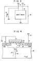
- Fig. 2 shows a semiconductor integrated circuit device including a MOS transistor having an LDD structure according to an embodiment of the present invention.
- a peripheral circuit (write circuit) of an EPROM will be described.
- an LDD structure is used in n- and p-channel MOS transistors to which a high voltage is applied.
- An operating power supply voltage Vcc from a power supply terminal 17, a high voltage power supply voltage Vpp for data write from a high voltage power supply terminal 18, and a power supply voltage Vss are respectively supplied to a write circuit 16.
- a protective MOS transistor Ql is connected between the high voltage power supply terminal 18 and the power supply Vss (ground), and the gate thereof is connected to ground Vss.
- the write circuit 16 and the protective MOS transistor Ql are formed on a single semiconductor substrate 19. Therefore, the write circuit 16 and the protective MOS transistor Ql can be simultaneously formed with the same process.
- Fig. 3 shows an arrangement of the write circuit in the device of Fig. 2.
- MOS transistors having the source and drain marked with circles have the LDD structure shown in Fig. 1.
- MOS transistors having either the source or drain marked with a circle have the LDD structure in which either the low impurity diffusion layer 13a or 13b in Fig. 1 is formed.
- An output terminal of an inverter 20 to which a write control signal PGM is supplied is connected to an input terminal of an inverter 21.
- An output terminal of the inverter 21 is connected to the gate of a p-channel MOS transistor Q3 through an n-channel MOS transistor Q2.
- the gate of the MOS transistor Q2 is connected to a power supply terminal 17a to which the operating power supply voltage Vcc is supplied.
- One end of the MOS transistor Q3 is connected to a high voltage power supply terminal 18a to which the high voltage power supply voltage Vpp is supplied, and the other end thereof is connected to one end of a MOS transistor Q4.
- the other end of the MOS transistor Q4 is connected to the ground Vss, and the gate thereof is connected to the output terminal of the inverter 21.
- a p-channel MOS transistor Q5 is connected between the gate of the MOS transistor Q3 and a high voltage power supply terminal 18b to which the high voltage power supply voltage Vpp is supplied.
- the gate of the MOS transistor Q5 is connected to a node between the MOS transistors Q3 and Q4.
- a write control circuit 22 is constituted by the inverters 20 and 21 and the MOS transistors Q2 to Q5.
- An output of the write control circuit 22 obtained from the node between the MOS transistors Q3 and Q4 is supplied to the gate of an n-channel MOS transistor Q6 which constitutes a switching circuit 23.
- One end of the MOS transistor Q6 is connected to a high voltage power supply terminal 18c to which the high voltage power supply voltage Vpp is supplied, and the other end thereof is connected to one end of an n-channel MOS transistor Q7.
- the other end of the MOS transistor Q7 is connected to a power supply terminal 17b to which the operating power supply voltage Vcc is supplied, and the write control signal PGM is supplied to the gate thereof.
- An outut of the switching circuit 23 obtained from a node between the MOS transistors Q6 and Q7 is supplied to X and Y decoders 24 and 25.
- the X and Y decoders 24 and 25 are respectively operated by the power supply voltages Vcc and Vss.
- An output from the X decoder 24 is supplied to the respective gates of MOS transistors QMl, QM2, ..., QMn having a floating gate structure.
- an output from the Y decoder 25 is supplied to the respective gates of n-channel MOS transistors QSl, QS2, ..., QSn for selecting the floating gate MOS transistors QMl, QM2, ..., QMn.
- a write signal is supplied to the memory cells MC1, MC2, ..., MCn from a data input circuit 26.
- the data input circuit 26 comprises an inverter 27 and MOS transistors Q8 to Q12.
- An output terminal of the inverter 27 to which data Din is supplied is connected to the gate of the MOS transistor Q8 and one end of the n-channel MOS transistor Q9.
- the other end of the MOS transistor Q9 is connected to the gate of the p-channel MOS transistor Q10, and the gate thereof is connected to the power supply terminal 17c to which the operating power supply voltage Vcc is supplid.
- the MOS transistors Q10 and Q8 are connected in series between a high voltage power supply terminal 18d to which the high voltage power supply voltage Vpp is supplied and the ground Vss.
- the p-channel MOS transistor Qll is connected between the gate of the MOS transistor Q10 and a high voltage power supply terminal 18e to which the high voltage power supply voltage Vpp is supplied.
- the gate of the MOS transistor Qll is connected to a node between the MOS transistors Q10 and Q8.
- the node between the MOS transistors Q10 and Q8 is also connected to the gate of the n-channel MOS transistor Q12.
- One end of the MOS transistor Q12 is connected to a high voltage power supply terminal 18f to which the high voltage power supply voltage Vpp is supplied, and the other end thereof is connected to the memory cells MCl, MC2, ..., MCn.
- the write control signal PGM is at level “0" in the data write mode and at level “1" in the data read mode
- the data Din is at level “0" in the write mode and at level "1" in the non-write mode.
- the MOS transistor Q4 is ON and the MOS transistor Q3 is OFF.
- the MOS transistor Q6 is OFF and the MOS transistor Q5 is ON.
- the MOS transistor Q7 is turned on when the write control signal PGM is at level "1"
- the power supply voltage Vcc is selected by the switching circuit 23, and the output from the switching circuit 23 is supplied to the X and Y decoders 24 and 25.
- the write control signal PGM is at level "0"
- the MOS transistor Q3 is ON and the MOS transistor Q4 is OFF.
- the MOS transistor Q6 is ON, and the MOS transistor Q5 is OFF.
- the switching circuit 23 selects the high voltage power supply Vpp.
- the output from the switching circuit 23 is supplied to the X and Y decoders 24 and 25.
- the MOS transistor Q8 is ON and the MOS transistor Q10 is OFF.
- the MOS transistor Q12 is OFF, and the MOS transistor Qll is ON.
- the gate insulating film of the MOS transistor with an LDD structure easily breaks down for the same reason as explained with reference to Fig. 1.
- the gate insulating film of the n-channel MOS transistor breaks down before that of the latter.
- Fig. 4 is a sectional view showing an arrangement of the protective transistor Q1 described above.
- n +- type impurity diffusion regions 29a and 29b respectively serving as a source S and a drain D are formed in a major surface region of a p-type semiconductor substrate 28 and are spaced by a predetermined distance.
- These impurity diffusion regions 29a and 29b can be simultaneously formed with the n +- type impurity diffusion regions (e.g., the n +- type impurity diffusion regions 12a and 12b in Fig. 1) of the MOS transistors having the LDD structure which constitute the write circuit 16.
- an impurity concentration of the impurity diffusion regions 29a and 29b is the same as that of the n +- type impurity diffusion regions 12a and 12b in the MOS transistor with an LDD structure, e.g., 1 x 10 20 cm -3 .
- An n-type impurity diffusion region 30 is formed between the n +- type impurity diffusion regions 29a and 29b so that one end of the region 30 contacts the region 29b.
- the n-type impurity diffusion region 30 can be simultaneously formed with the n - -type impurity diffusion regions 13a and 13b.
- An impurity concentration of the n - -type impurity diffusion region 30 is the same as that of the n - -type impurity diffusion regions 13a and 13b in the MOS transistor with an LDD structure, e.g., 1 x 10 17 c m- 3 to 1 x 10 18 cm- 3 .
- a gate insulating film 31, e.g., a silicon oxide film of a thickness of 500 A is formed on a major surface of the semiconductor substrate 28 between the impurity diffusion regions 29a and 30.
- a gate electrode 32 is formed on the gate insulating film 31.
- the gate insulating film 31 and the gate electrode 32 are formed in the same step as that of the gate insulating film 14 and the gate electrode 15 of the MOS transistor of the LDD structure in Fig. 1.
- a high voltage power supply terminal 18 to which the high voltage power supply voltage Vpp is supplied is connected to the n +- type impurity diffusion region 29b as the drain D.
- the gate electrode 32 and the n +- type impurity diffusion region 29a as the source S are connected to ground Vss.
- a parasitic bipolar transistor in which the n +- type impurity diffusion region 29b (drain D), the n +- type impurity diffusion region 29a (source S) and the p-type semiconductor substrate 28 respectively serve as a collector, an emitter and a base is turned on.
- the source S is connected to the ground Vss and the parasitic bipolar transistor has a minimal ON resistance, the surge voltage applied to the high voltage power supply terminal 18 can be quickly discharged. Therefore, a surge withstand voltage of the MOS transistors with an LDD structure which constitute the write circuit 16 can be improved.
- a protective parasitic bipolar transistor can be formed between other impurity diffusion regions.
- Fig. 5 shows a structure of a parasitic bipolar transistor QB which is constituted by the semiconductor substrate 28 and one of the source S and the drain D of each of the two adjacent MOS transistors isolated by a field oxide film 35.
- the parasitic bipolar transistor QB has an n +- type impurity diffusion region 36 (the source S) as an emitter, an n + -type impurity diffusion region 37 (the drain D) as a collector and the p-type semiconductor substrate 28 as a base.
- Fig. 6 shows another embodiment of the present invention, i.e., a structure where a protective transistor is formed in a CMOS circuit in which a p-type well region 39 is formed in an n-type semiconductor substrate 38.
- An n + -type impurity diffusion region 40 formed in the p-type well region 39 is connected to a high voltage power supply terminal 18 to which a high voltage power supply voltage Vpp is supplied.
- p +- type impurity diffusion regions 41a and 41b which are formed in the p-type well region 39 are connected to the ground Vss.
- n +- type impurity diffusion region 40, the well region 39 and the semiconductor substrate 38 respectively serve as an emitter, a base and a collector of a parasitic bipolar transistor QB.
- reference symbol Rw denotes a base resistance (the resistance of the well region 39).
- a parasitic bipolar transistor in which the semiconductor substrate (n-type) 38, the well region (p-type) and the p +- type impurity diffusion region 40 respectively serve as a collector, a base and an emitter can be formed.
- Fig. 7 is a graph showing measurements of a withstand voltage as a function of a channel width of a protective transistor.
- the protective transistor is formed in such a manner that an aluminum gate is formed in the transistor shown in Fig. 5 so as to form an aluminum field transistor therefor.
- a channel length L is a constant value, i.e., 4 ⁇ m.
- the aluminum gate is grounded, a 200 pF capacitor is charged with a predetermined voltage, and an electric charge of this capacitor is applied to a high voltage power supply terminal 18 as a surge voltage.
- reference symbols. , x, A ⁇ and o respectively indicate different lot numbers.
- a channel width W 0 ⁇ m
- the withstand voltage is distributed within a wide range between 100 to 550 V.
- the withstand voltage can be improved in accordance with an increase in the channel width W thereof. For example, in order to obtain a withstand voltage of 300 V, a protective transistor having a channel width of 250 ⁇ m or more (when the channel length L is 4 ⁇ m) can be formed.
- the present invention is effective for protecting a ROM except for a non-volatile memory such as an E 2 PROM; a dynamic RAM; a static RAM; and a power supply system or a data output system of a microprocessor and the like from a surge voltage.
- a non-volatile memory such as an E 2 PROM
- a dynamic RAM such as an E 2 PROM
- a static RAM such as an E 2 PROM
- a power supply system or a data output system of a microprocessor and the like from a surge voltage.
- the above LDD structure is very important to cause a power supply voltage for the IC to be decreased to 5 V, and the present invention can be applied to all micropatterned semiconductor integrated circuit devices having the LDD structure.
- the protective transistor is provided between the ground Vss and the high voltage power supply terminal 18 to which the high voltage power supply voltage Vpp is supplied.
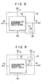
- a protective transistor can be provided between the output terminal and the ground. Referring to Fig. 8, a semiconductor integrated circuit 42 having MOS transistors with an LDD structure is operated by applying the power supply voltages Vcc and Vss. An input signal IN from an input terminal 43 is supplied to the semiconductor integrated circuit 42 so as to obtain an output signal OUT from an output terminal 44.
- a protective MOS transistor Ql is connected between the output terminal 44 and the ground Vss, and the gate thereof is connected to the ground Vss.
- the protective MOS transistor Ql can be formed on the same semiconductor substrate 45 as the semiconductor integrated circuit 42, and the structure thereof can be the same as those shown in Figs. 4 to 6.
- the MOS transistor Ql can be connected between the output terminal 44 and the power supply terminal 17 to which the operating power supply voltage Vcc is supplied, as shown in Fig. 9.
- the gate and back gate of the MOS transistor Ql are connected to the power supply terminal 17.
Landscapes
- Engineering & Computer Science (AREA)
- Power Engineering (AREA)
- Metal-Oxide And Bipolar Metal-Oxide Semiconductor Integrated Circuits (AREA)
- Amplifiers (AREA)
- Non-Volatile Memory (AREA)
- Protection Of Static Devices (AREA)
- Insulated Gate Type Field-Effect Transistor (AREA)
Applications Claiming Priority (2)
| Application Number | Priority Date | Filing Date | Title |
|---|---|---|---|
| JP59063686A JPS60207383A (ja) | 1984-03-31 | 1984-03-31 | 半導体装置 |
| JP63686/84 | 1984-03-31 |
Publications (2)
| Publication Number | Publication Date |
|---|---|
| EP0161446A2 true EP0161446A2 (de) | 1985-11-21 |
| EP0161446A3 EP0161446A3 (de) | 1986-11-26 |
Family
ID=13236500
Family Applications (1)
| Application Number | Title | Priority Date | Filing Date |
|---|---|---|---|
| EP85103819A Withdrawn EP0161446A3 (de) | 1984-03-31 | 1985-03-29 | Integrierte Halbleiterschaltung mit einem Schutztransistor und einem MOS-Transistor mit einer LDD-Struktur |
Country Status (2)
| Country | Link |
|---|---|
| EP (1) | EP0161446A3 (de) |
| JP (1) | JPS60207383A (de) |
Cited By (8)
| Publication number | Priority date | Publication date | Assignee | Title |
|---|---|---|---|---|
| EP0292327A3 (de) * | 1987-05-22 | 1990-06-13 | Sony Corporation | Schutzschaltungen gegen elektrostatischen Durchbruch |
| EP0434850A4 (en) * | 1989-07-18 | 1991-10-02 | Seiko Instruments Inc. | Semiconductor device |
| EP0470371A3 (en) * | 1990-07-06 | 1992-07-01 | Kabushiki Kaisha Toshiba | Semiconductor device with input protection circuit of high withstand voltage |
| US5208475A (en) * | 1991-01-30 | 1993-05-04 | National Semiconductor Corporation | Electrostatic discharge protection device and a method for simultaneously forming MOS devices with both lightly doped and non lightly doped source and drain regions |
| US5246872A (en) * | 1991-01-30 | 1993-09-21 | National Semiconductor Corporation | Electrostatic discharge protection device and a method for simultaneously forming MOS devices with both lightly doped and non lightly doped source and drain regions |
| US5345103A (en) * | 1989-07-18 | 1994-09-06 | Seiko Instruments Inc. | Gate controlled avalanche bipolar transistor |
| EP0590859A3 (en) * | 1992-09-28 | 1995-11-22 | Xerox Corp | Office environment level electrostatic discharge protection |
| EP0772238A3 (de) * | 1995-10-31 | 1999-11-24 | Texas Instruments Incorporated | Halbleiteranordnung mit einem Schutzmittel |
Families Citing this family (2)
| Publication number | Priority date | Publication date | Assignee | Title |
|---|---|---|---|---|
| US5257095A (en) * | 1985-12-04 | 1993-10-26 | Advanced Micro Devices, Inc. | Common geometry high voltage tolerant long channel and high speed short channel field effect transistors |
| JPH07105446B2 (ja) * | 1988-01-11 | 1995-11-13 | 株式会社東芝 | Mos型半導体装置の入力保護回路 |
Family Cites Families (6)
| Publication number | Priority date | Publication date | Assignee | Title |
|---|---|---|---|---|
| US3512058A (en) * | 1968-04-10 | 1970-05-12 | Rca Corp | High voltage transient protection for an insulated gate field effect transistor |
| US3739238A (en) * | 1969-09-24 | 1973-06-12 | Tokyo Shibaura Electric Co | Semiconductor device with a field effect transistor |
| JPS526470U (de) * | 1975-06-30 | 1977-01-18 | ||
| IT1150062B (it) * | 1980-11-19 | 1986-12-10 | Ates Componenti Elettron | Protezione di ingresso per circuito integrato di tipo mos, a bassa tensione di alimentazione e ad alta densita' di integrazione |
| NL8100347A (nl) * | 1981-01-26 | 1982-08-16 | Philips Nv | Halfgeleiderinrichting met een beveiligingsinrichting. |
| US4602267A (en) * | 1981-02-17 | 1986-07-22 | Fujitsu Limited | Protection element for semiconductor device |
-
1984
- 1984-03-31 JP JP59063686A patent/JPS60207383A/ja active Granted
-
1985
- 1985-03-29 EP EP85103819A patent/EP0161446A3/de not_active Withdrawn
Cited By (10)
| Publication number | Priority date | Publication date | Assignee | Title |
|---|---|---|---|---|
| EP0292327A3 (de) * | 1987-05-22 | 1990-06-13 | Sony Corporation | Schutzschaltungen gegen elektrostatischen Durchbruch |
| EP0434850A4 (en) * | 1989-07-18 | 1991-10-02 | Seiko Instruments Inc. | Semiconductor device |
| US5345103A (en) * | 1989-07-18 | 1994-09-06 | Seiko Instruments Inc. | Gate controlled avalanche bipolar transistor |
| EP0470371A3 (en) * | 1990-07-06 | 1992-07-01 | Kabushiki Kaisha Toshiba | Semiconductor device with input protection circuit of high withstand voltage |
| US5210436A (en) * | 1990-07-06 | 1993-05-11 | Kabushiki Kaisha Toshiba | Semiconductor device with input protection circuit of high withstand voltage |
| US5208475A (en) * | 1991-01-30 | 1993-05-04 | National Semiconductor Corporation | Electrostatic discharge protection device and a method for simultaneously forming MOS devices with both lightly doped and non lightly doped source and drain regions |
| US5246872A (en) * | 1991-01-30 | 1993-09-21 | National Semiconductor Corporation | Electrostatic discharge protection device and a method for simultaneously forming MOS devices with both lightly doped and non lightly doped source and drain regions |
| EP0590859A3 (en) * | 1992-09-28 | 1995-11-22 | Xerox Corp | Office environment level electrostatic discharge protection |
| US5532901A (en) * | 1992-09-28 | 1996-07-02 | Xerox Corporation | Office environment level electrostatic discharge protection |
| EP0772238A3 (de) * | 1995-10-31 | 1999-11-24 | Texas Instruments Incorporated | Halbleiteranordnung mit einem Schutzmittel |
Also Published As
| Publication number | Publication date |
|---|---|
| EP0161446A3 (de) | 1986-11-26 |
| JPS60207383A (ja) | 1985-10-18 |
| JPH0464186B2 (de) | 1992-10-14 |
Similar Documents
| Publication | Publication Date | Title |
|---|---|---|
| US4378506A (en) | MIS Device including a substrate bias generating circuit | |
| KR100190008B1 (ko) | 반도체 장치의 정전하 보호 장치 | |
| US4665418A (en) | Semiconductor memory device | |
| US4798974A (en) | Integrated circuit comprising a latch-up protection circuit in complementary MOS-circuitry technology | |
| JPH09181195A (ja) | 静電気保護素子 | |
| JP2528794B2 (ja) | ラツチアツプ保護回路付き集積回路 | |
| US4733285A (en) | Semiconductor device with input and/or output protective circuit | |
| JP3001454B2 (ja) | 半導体装置 | |
| US4143391A (en) | Integrated circuit device | |
| EP0213608A2 (de) | Halbleiterschalter | |
| EP0361546B1 (de) | Halbleiterspeichereinrichtung | |
| US4725875A (en) | Memory cell with diodes providing radiation hardness | |
| JPH0464186B2 (de) | ||
| KR860000159B1 (ko) | 반도체 메모리 | |
| US4692785A (en) | Integrated circuit device for writing and reading information | |
| US4868628A (en) | CMOS RAM with merged bipolar transistor | |
| US5942931A (en) | Circuit for protecting an IC from noise | |
| US4725915A (en) | Semiconductor integrated circuit | |
| EP0184222B1 (de) | MOS-Typ integrierte Schaltung mit Ladungs- und Entladungstransistoren | |
| JP2679046B2 (ja) | メモリ装置 | |
| KR0149226B1 (ko) | 반도체 회로를 위한 정전기 보호장치 | |
| KR900002886B1 (ko) | 반도체 기억장치 | |
| US4887135A (en) | Dual level polysilicon single transistor-capacitor memory array | |
| JP2702909B2 (ja) | 半導体集積回路装置 | |
| JPH10334677A (ja) | 不揮発性半導体メモリ |
Legal Events
| Date | Code | Title | Description |
|---|---|---|---|
| PUAI | Public reference made under article 153(3) epc to a published international application that has entered the european phase |
Free format text: ORIGINAL CODE: 0009012 |
|
| 17P | Request for examination filed |
Effective date: 19850329 |
|
| AK | Designated contracting states |
Designated state(s): DE FR GB |
|
| PUAL | Search report despatched |
Free format text: ORIGINAL CODE: 0009013 |
|
| AK | Designated contracting states |
Kind code of ref document: A3 Designated state(s): DE FR GB |
|
| STAA | Information on the status of an ep patent application or granted ep patent |
Free format text: STATUS: THE APPLICATION IS DEEMED TO BE WITHDRAWN |
|
| 18D | Application deemed to be withdrawn |
Effective date: 19881001 |
|
| RIN1 | Information on inventor provided before grant (corrected) |
Inventor name: TSUSHIMA, TOSHIKIC/O PATENT DIVISION Inventor name: TANAKA, SUMIOC/O PATENT DIVISION Inventor name: ATSUMI, SHIGERUC/O PATENT DIVISION Inventor name: TOZAWA, NORIYOSHIC/O PATENT DIVISION Inventor name: OKUDA, TAIZOC/O PATENT DIVISION Inventor name: ASANO, MASAMICHIC/O PATENT DIVISION |