EP0162653A2 - Buseinrichtung zur Adressierung von Geräten und deren Verfahren - Google Patents
Buseinrichtung zur Adressierung von Geräten und deren Verfahren Download PDFInfo
- Publication number
- EP0162653A2 EP0162653A2 EP85303389A EP85303389A EP0162653A2 EP 0162653 A2 EP0162653 A2 EP 0162653A2 EP 85303389 A EP85303389 A EP 85303389A EP 85303389 A EP85303389 A EP 85303389A EP 0162653 A2 EP0162653 A2 EP 0162653A2
- Authority
- EP
- European Patent Office
- Prior art keywords
- bus
- address
- unit
- rack
- arrangement
- Prior art date
- Legal status (The legal status is an assumption and is not a legal conclusion. Google has not performed a legal analysis and makes no representation as to the accuracy of the status listed.)
- Withdrawn
Links
Images


Classifications
-
- G—PHYSICS
- G06—COMPUTING OR CALCULATING; COUNTING
- G06F—ELECTRIC DIGITAL DATA PROCESSING
- G06F12/00—Accessing, addressing or allocating within memory systems or architectures
- G06F12/02—Addressing or allocation; Relocation
- G06F12/06—Addressing a physical block of locations, e.g. base addressing, module addressing, memory dedication
- G06F12/0646—Configuration or reconfiguration
- G06F12/0669—Configuration or reconfiguration with decentralised address assignment
- G06F12/0676—Configuration or reconfiguration with decentralised address assignment the address being position dependent
-
- G—PHYSICS
- G06—COMPUTING OR CALCULATING; COUNTING
- G06T—IMAGE DATA PROCESSING OR GENERATION, IN GENERAL
- G06T3/00—Geometric image transformations in the plane of the image
- G06T3/02—Affine transformations
Definitions
- This invention relates generally to a bus arrangement for providing equipment units with an address and more particularly to a a bus arrangement wherein each individual unit achieves its address automatically according to its relative physical position within the organization of the equipment units without the need for setting any switches (or the like).
- the present invention is directed to automatically providing an address for each equipment unit as it is connected to other equipment units and thereby reducing the chance of operator error.
- the present invention employs a unique addressing bus.
- This unique addressing bus is the same in each equipment unit.
- the input side (entry port) of the address bus receives signals from an adjacent equipment unit and transfers these signals to an output termination (exit port).
- the address bus is modified such that one input lead becomes terminated and a ground lead is picked up. This will be explained in more detail in the figures accompanying this description.
- the present invention is a bus arrangement for interconnecting a plurality of equipment units in such a fashion that each unit is given a unique address, dependent solely upon its relative position to other equipment units in the interconnection, the bus arrangement in each unit comprising: an entry port having N terminals, N being a positive integer equal to or greater than two; an exit port having N terminals corresponding respectively to the N terminals of the entry port, wherein the 2nd to N th terminals s of the entry port are connected to the ist to (N-1) th terminals, respectively, of the exit port, and an originating connection is made to the N th terminal of the exit port.
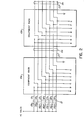
- FIG. 1 depicts eight equipment racks 10a through 10h and referred to collectively as equipment racks (or equipment units) 10.
- Equipment racks 10a through 10h are interconnected with buses llb through llh respectively as shown in Figure 1.
- Buses 11b through llh are referred to collectively as buses 11 and are identical one with another.
- Bus 12 applies the initial address bus to rack 10a as shown.
- each equipment rack 10 receives its address according to its position relative to bus 12; that is, rack 10a achieves a particular address because it is the rack that receives bus 12.
- Equipment rack 10b receives its address because it is the one connected to rack 10a.
- rack 10c achieves its address solely due to the fact that it is the one connected to rack 10b etc., all the way through to 10h. This is shown in more detail in Figure 2 to which attention is directed.
- Bus 12 is comprised of leads 13, 14, 15, 16, 17, 18 and 19 as depicted in Figure 2 and are connected to a plus five volt supply via resistors 13a, 14a, 15a, 16a, 17a, 18a, and 19a respectively (note: each resistor 13a to 19a inclusive is 5.1 Kohms).
- the address of equipment rack 10a is given in the bottom of the block as A B C D E F G which of course in this illustrative embodiment is logic 1111111. It will also be noted that after the address of equipment rack 10a is established, lead 13 terminates. It will also be noted that leads 14 through 19 continue through equipment rack 10a and are shifted up one place position such that when they cross to equipment rack 10b, via bus 11b, their position is one above what it was when it entered equipment rack 10a, and in addition a new lead (a ground lead) indicated as lead 21 is added. This provides an address for equipment rack 10b, once again of A B C D E F G which is now logic 1111110.
- each equipment rack 10 receives a unique address dependent only upon its physical position within the assembly of racks.
- the seven bit binary number used to address the racks may prove to be somewhat cumbersome.
- an encoding scheme may be used to reduce the address to a three digit binary number within a rack 10 itself.
- This encoding scheme is implemented by an 8-line to 3-line encoder such as a model SN74LS148.
- the end result of this encoding scheme is depicted in Table I wherein there is shown both an unencoded address for each equipment rack 10 as well as an encoded address.
- equipment rack 10a has an unencoded address of 1 1 1 1 1 1 1 and an encoded address of 1 1 1. Similar results for the other racks 10 can be found in Table I.
- Each rack 10 may be subdivided into eight slots. These eight slots are represented in Figure 3 with the four slots running from left to right on the top of rack 10a, being indicated as slots 1 through 4 and the four slots on thf bottom of rack 10a being indicated as 5 through 8. When addressing, these slots can each have a unique address; for example, a three digit tinary number running from 0 0 0 to 1 1 1. This would of course necessitate three additional lines on the address buses llb and lie etc., shown in Figures 1 and 2.
- Table II Attention is directed to Table II wherein there are depicted the unencoded addresses and the encoded addresses for the racks 10 when the slot numbers are als taken into account. As can be seen from Table II, the last three digits of each address (encoded or unencoded) is the slot address.
- Figure 4 depicts a further arrangement of three equipment racks 30a, 30b, and 30c referred to collectively as racks 30.
- the principle of operation is the same as the Figure 2 embodiment.
- the interconnecting buses i.e. buses 31b and 31c
- input bus 32 have only two leads.
- addresses can be provided; namely logic 11, logic 10, and logic 00.
- rack 30a achieves an address of logic 11
- rack 30b achieves an address of logic 10
- rack 30c achieves an address of logic 00.
- Input bus 32 is connected to a plus five volt supply via 5.1 Kohm resistors 33a and 33b.
- Figure 5 is similar to Figure 4 except that input bus 42 is logic 0 (i.e. grouid, instead of plus five volts). Consequently, the address of rack 40a is logic 00. Interconnecting bus 41b joins racks 40a and 40b, and interconnecting bus 41c joins racks 40b and 40c. The address of rack 40b is logic 01 since one lead of bus 41b applies plus five volts from resistor 43a. The address of rack 40c is logic 11 since now both leads of bus 41c carry plus five volts (from resistors 43a and 43b).
Landscapes
- Engineering & Computer Science (AREA)
- Theoretical Computer Science (AREA)
- Physics & Mathematics (AREA)
- General Physics & Mathematics (AREA)
- General Engineering & Computer Science (AREA)
- Small-Scale Networks (AREA)
- Details Of Connecting Devices For Male And Female Coupling (AREA)
Applications Claiming Priority (2)
| Application Number | Priority Date | Filing Date | Title |
|---|---|---|---|
| US06/613,062 US4626846A (en) | 1984-05-22 | 1984-05-22 | Bus arrangement for addressing equipment units and a method therefor |
| US613062 | 2003-07-03 |
Publications (2)
| Publication Number | Publication Date |
|---|---|
| EP0162653A2 true EP0162653A2 (de) | 1985-11-27 |
| EP0162653A3 EP0162653A3 (de) | 1988-07-20 |
Family
ID=24455713
Family Applications (1)
| Application Number | Title | Priority Date | Filing Date |
|---|---|---|---|
| EP85303389A Withdrawn EP0162653A3 (de) | 1984-05-22 | 1985-05-14 | Buseinrichtung zur Adressierung von Geräten und deren Verfahren |
Country Status (5)
| Country | Link |
|---|---|
| US (1) | US4626846A (de) |
| EP (1) | EP0162653A3 (de) |
| JP (1) | JPS60254265A (de) |
| KR (1) | KR850008062A (de) |
| CA (1) | CA1220831A (de) |
Cited By (3)
| Publication number | Priority date | Publication date | Assignee | Title |
|---|---|---|---|---|
| EP0340325A1 (de) * | 1988-05-05 | 1989-11-08 | Hewlett-Packard GmbH | Digitaladressierbare elektronische Vorrichtung |
| EP0843260A1 (de) * | 1996-11-15 | 1998-05-20 | Digital Equipment Corporation | Automatische Adressenzuweisung für Plattenlaufwerken enthaltende Gestelle sowie Fehlererkennungsverfahren und Gerät |
| WO2010127917A1 (de) * | 2009-05-06 | 2010-11-11 | Robert Bosch Gmbh | Sensor-system und verfahren zum betreiben eines sensor-systems |
Families Citing this family (25)
| Publication number | Priority date | Publication date | Assignee | Title |
|---|---|---|---|---|
| US4689786A (en) * | 1985-03-21 | 1987-08-25 | Apple Computer, Inc. | Local area network with self assigned address method |
| US4875158A (en) * | 1985-08-14 | 1989-10-17 | Apple Computer, Inc. | Method for requesting service by a device which generates a service request signal successively until it is serviced |
| US4918598A (en) * | 1985-08-14 | 1990-04-17 | Apple Computer, Inc. | Method for selectively activating and deactivating devices having same first address and different extended addresses |
| US4912627A (en) * | 1985-08-14 | 1990-03-27 | Apple Computer, Inc. | Method for storing a second number as a command address of a first peripheral device and a third number as a command address of a second peripheral device |
| US4910655A (en) * | 1985-08-14 | 1990-03-20 | Apple Computer, Inc. | Apparatus for transferring signals and data under the control of a host computer |
| US4811275A (en) * | 1986-05-28 | 1989-03-07 | Unisys Corporation | Addressing system for an expandable modular electromechanical memory assembly |
| US5539390A (en) * | 1990-07-19 | 1996-07-23 | Sony Corporation | Method for setting addresses for series-connectd apparatuses |
| US5204669A (en) * | 1990-08-30 | 1993-04-20 | Datacard Corporation | Automatic station identification where function modules automatically initialize |
| US5210531A (en) * | 1991-03-02 | 1993-05-11 | Fordham Richard J | Monitoring and control system with binary addressing |
| US5160276A (en) * | 1991-07-09 | 1992-11-03 | Group Dekko International | Modular communication interconnection system |
| NL9102198A (nl) * | 1991-12-31 | 1993-07-16 | Hadewe Bv | Werkwijze voor het besturen van een postsamenstellingsinrichting alsmede inrichting en hulpmiddelen voor het toepassen van die werkwijze. |
| JP2963812B2 (ja) * | 1992-02-27 | 1999-10-18 | 富士通株式会社 | 識別番号自動設定式回路カード装着シェルフ装置 |
| US5719933A (en) * | 1994-02-18 | 1998-02-17 | Welch; Richard | Wiring arrangement for a communication interconnection system |
| US5613158A (en) * | 1994-05-25 | 1997-03-18 | Tandem Computers, Inc. | System for specifying addresses by creating a multi-bit ranked ordered anchor pattern and creating next address by shifting in the direction of the superior position |
| US5576698A (en) * | 1994-09-22 | 1996-11-19 | Unisys Corporation | Physical addressing of modules |
| US5629685A (en) * | 1995-02-23 | 1997-05-13 | International Business Machines Corporation | Segmentable addressable modular communication network hubs |
| US5680113A (en) * | 1995-02-24 | 1997-10-21 | International Business Machines Corporation | Dynamic address assignments to serially connected devices |
| US6537109B1 (en) * | 1997-01-16 | 2003-03-25 | Hewlett-Packard Company | Chainable I/O termination block system |
| US6174196B1 (en) * | 1998-09-30 | 2001-01-16 | Lucent Technologies Inc. | Low-cost multi-shelf cabling arrangement |
| US6795871B2 (en) | 2000-12-22 | 2004-09-21 | General Electric Company | Appliance sensor and man machine interface bus |
| JP4794218B2 (ja) * | 2004-06-25 | 2011-10-19 | パナソニック株式会社 | スレーブ装置、マスタ装置及び積層装置 |
| US20060061493A1 (en) * | 2004-09-22 | 2006-03-23 | Larson Lee A | Apparatus and method for assigning circuit card base addresses using thermometer codes |
| US8325010B2 (en) * | 2010-02-05 | 2012-12-04 | Emerson Electric Co. | Physical addressing for transient voltage surge suppressor modules |
| US9217995B2 (en) * | 2012-07-23 | 2015-12-22 | Brian W. Karam | Entertainment, lighting and climate control system |
| CN103176418B (zh) * | 2013-03-08 | 2015-08-19 | 深圳市泰昂能源科技股份有限公司 | 电力系统智能馈线开关模组的地址编码方法 |
Family Cites Families (4)
| Publication number | Priority date | Publication date | Assignee | Title |
|---|---|---|---|---|
| DE2348002C3 (de) * | 1973-09-24 | 1979-12-20 | Siemens Ag, 1000 Berlin Und 8000 Muenchen | Modular aufgebaute Datenverarbeitungsanlage mit einer Anzahl von gleichartigen Prozessoren für die DateneinVausgabe |
| US4443866A (en) * | 1975-08-27 | 1984-04-17 | Corning Glass Works | Automatic device selection circuit |
| US4016369A (en) * | 1976-03-09 | 1977-04-05 | Bell Telephone Laboratories, Incorporated | Addressing arrangements for communications networks |
| US4253087A (en) * | 1979-03-08 | 1981-02-24 | Nestar Systems Incorporated | Self-assigning address system |
-
1984
- 1984-05-22 US US06/613,062 patent/US4626846A/en not_active Expired - Fee Related
- 1984-08-30 CA CA000462095A patent/CA1220831A/en not_active Expired
-
1985
- 1985-05-14 EP EP85303389A patent/EP0162653A3/de not_active Withdrawn
- 1985-05-20 KR KR1019850003444A patent/KR850008062A/ko not_active Ceased
- 1985-05-21 JP JP60107080A patent/JPS60254265A/ja active Pending
Cited By (3)
| Publication number | Priority date | Publication date | Assignee | Title |
|---|---|---|---|---|
| EP0340325A1 (de) * | 1988-05-05 | 1989-11-08 | Hewlett-Packard GmbH | Digitaladressierbare elektronische Vorrichtung |
| EP0843260A1 (de) * | 1996-11-15 | 1998-05-20 | Digital Equipment Corporation | Automatische Adressenzuweisung für Plattenlaufwerken enthaltende Gestelle sowie Fehlererkennungsverfahren und Gerät |
| WO2010127917A1 (de) * | 2009-05-06 | 2010-11-11 | Robert Bosch Gmbh | Sensor-system und verfahren zum betreiben eines sensor-systems |
Also Published As
| Publication number | Publication date |
|---|---|
| CA1220831A (en) | 1987-04-21 |
| JPS60254265A (ja) | 1985-12-14 |
| KR850008062A (ko) | 1985-12-11 |
| EP0162653A3 (de) | 1988-07-20 |
| US4626846A (en) | 1986-12-02 |
Similar Documents
| Publication | Publication Date | Title |
|---|---|---|
| EP0162653A2 (de) | Buseinrichtung zur Adressierung von Geräten und deren Verfahren | |
| US5613158A (en) | System for specifying addresses by creating a multi-bit ranked ordered anchor pattern and creating next address by shifting in the direction of the superior position | |
| US5148389A (en) | Modular expansion bus configuration | |
| US4443866A (en) | Automatic device selection circuit | |
| EP0118978A3 (de) | Adressenablaufsteuerung für eine Musterverarbeitungsanlage | |
| US4429414A (en) | Pattern recognition system operating by the multiple similarity method | |
| US5153843A (en) | Layout of large multistage interconnection networks technical field | |
| ES8704063A1 (es) | Red de commutacion de paquetes de etapas multiples. | |
| US5786777A (en) | Data compression communication method between a main control unit and terminals | |
| US4349702A (en) | Nodal switching network with binary order links | |
| US4733216A (en) | N+1 bit resolution from an N bit A/D converter | |
| CA2090567A1 (en) | Method of and apparatus for data distribution | |
| US3993980A (en) | System for hard wiring information into integrated circuit elements | |
| US6516377B1 (en) | Self-configuring modular electronic system | |
| DE19701508C2 (de) | Selbstkonfigurierendes modulares Elektroniksystem, insbesondere Computersystem | |
| CA1101971A (en) | Trunk control system | |
| US4327418A (en) | High speed information selection and transfer system | |
| EP0322075A3 (de) | Koppelfeld und Koppelfeldsteuerung für ein Vermittlungssystem | |
| US3246315A (en) | Read only memory | |
| US4015244A (en) | Selective addressing system | |
| KR920005094Y1 (ko) | 프로그래머블 콘트롤러의 입출력 랙 및 카드 선택장치 | |
| US3568159A (en) | Multimatch processing system | |
| US4132866A (en) | Concentration network for a time division multiplex telephone exchange with pulse amplitude modulation | |
| SU1472949A1 (ru) | Программируема логическа матрица | |
| SU1383334A1 (ru) | Устройство дл выбора экстремального из @ @ -разр дных двоичных чисел |
Legal Events
| Date | Code | Title | Description |
|---|---|---|---|
| PUAI | Public reference made under article 153(3) epc to a published international application that has entered the european phase |
Free format text: ORIGINAL CODE: 0009012 |
|
| AK | Designated contracting states |
Designated state(s): AT DE FR GB IT NL |
|
| PUAL | Search report despatched |
Free format text: ORIGINAL CODE: 0009013 |
|
| AK | Designated contracting states |
Kind code of ref document: A3 Designated state(s): AT DE FR GB IT NL |
|
| 17P | Request for examination filed |
Effective date: 19890120 |
|
| 17Q | First examination report despatched |
Effective date: 19900705 |
|
| STAA | Information on the status of an ep patent application or granted ep patent |
Free format text: STATUS: THE APPLICATION IS DEEMED TO BE WITHDRAWN |
|
| 18D | Application deemed to be withdrawn |
Effective date: 19901116 |
|
| RIN1 | Information on inventor provided before grant (corrected) |
Inventor name: PARKER, JAY SCOTT Inventor name: KOZIOL, LEO BERNARD |