EP0163275A2 - Circuit d'alimentation pour une ligne d'abonné - Google Patents
Circuit d'alimentation pour une ligne d'abonné Download PDFInfo
- Publication number
- EP0163275A2 EP0163275A2 EP85106415A EP85106415A EP0163275A2 EP 0163275 A2 EP0163275 A2 EP 0163275A2 EP 85106415 A EP85106415 A EP 85106415A EP 85106415 A EP85106415 A EP 85106415A EP 0163275 A2 EP0163275 A2 EP 0163275A2
- Authority
- EP
- European Patent Office
- Prior art keywords
- feed circuit
- resistor
- resistors
- transistor
- battery feed
- Prior art date
- Legal status (The legal status is an assumption and is not a legal conclusion. Google has not performed a legal analysis and makes no representation as to the accuracy of the status listed.)
- Granted
Links
Images






Classifications
-
- H—ELECTRICITY
- H04—ELECTRIC COMMUNICATION TECHNIQUE
- H04M—TELEPHONIC COMMUNICATION
- H04M19/00—Current supply arrangements for telephone systems
-
- H—ELECTRICITY
- H04—ELECTRIC COMMUNICATION TECHNIQUE
- H04M—TELEPHONIC COMMUNICATION
- H04M19/00—Current supply arrangements for telephone systems
- H04M19/001—Current supply source at the exchanger providing current to substations
- H04M19/005—Feeding arrangements without the use of line transformers
Definitions
- the present invention relates to a battery feed circuit, more particularly, to a battery feed circuit for use as a constant-current battery feed circuit for subscriber lines in a switching system.
- battery feed circuits play an important role in feeding a constant DC current, via subscriber lines, to telephone sets, data terminals, and other subscriber units. Battery feed circuits are thus some of the most important parts in a switching system.
- Constant-resistor types are not very practical from the viewpoint of power consumption.
- Constant-current types feature lower power consumption, but suffer from the problem of instability and undesired clipping of transmission signals due to common mode noise induced along the subscriber lines.
- An object of the present invention is to provide an improved battery feed circuit installed in a line circuit for a subscriber line in a switching system, which will work to feed DC current as usual and further suppress noise in the transmission signals.
- the battery feed circuit according to the present invention incorporates special means for balancing the subscriber line pair in voltage potential.
- FIG. 1 is a general circuit diagram of an example of a conventional subscriber line in, for example, a digital switching system.
- ringing circuit operative to send ringing signals (given from a continuous ringer CR) to a subscriber unit U (in the drawing, U is a telephone set) connected, via subscriber lines A and B, with the circuit LC.
- the transmission signal to and from the subscriber unit U is transferred by way of a hybrid transformer H for performing conversion between a two-wire line provided with a DC-cut capacitor C and a four-wire line provided with a balancing network BN.
- the hybrid transformer H is connected, via a codec (coder-decoder) CD comprised of both an analog/digital (A/D) converter and a digital/analog (D/A) converter, to a digital switching network NW.
- the codec CD works to effect conversions between a usual voice signal and pulse code modulation (PCM) signal.
- PCM pulse code modulation
- the continuous ringer CR cooperates with a scanner SCN.
- the scanner SCN is also connected with a supervisory circuit S.
- Reference character T denotes a test circuit connected with test configuration lines TST.
- the battery feed circuit BF is connected with the subscriber lines A and B and supplies DC current thereto during an off-hook state. During this state, the battery feed circuit BF provides a high impedance so as to prevent attenuation of the AC transmission signals, e.g., voice signals.
- Figure 2(a) is a circuit diagram of a conventional constant-resistor type feed circuit
- Fig. 2(b) is a graph depicting DC voltage-current characteristics of the subscriber line A and B.
- the subscriber line A and a power source of -V BB are provided with the series-connected resistor R 1 and inductance L 1 therebetween, while the subscriber line B and a ground GD are provided with the series-connected resistor R 2 and inductance L 2 therebetween.
- the members R1 and L 1 form a battery feed circuit B a
- the members R 2 and L 2 form a battery feed circuit B b .
- the inductance L 1 and L 2 represent respective coils for feeding DC current.
- each of the coils L 1 and L 2 provides a sufficiently large inductance for frequencies higher than 300 Hz of the voice signals, a high impedance state can be achieved.
- the coils exhibit a low impedance against a DC current, defined by the resistors R 1 and R 2 .
- the battery feeding current I is stabilized, such as shown in Fig. 2(b), wherein line b represents a voltage-current characteristic regarding the subscriber line B and line A represents the same regarding the subscriber line A.
- the intermediate voltage between the subscriber lines A and B is held at -V BB /2 during the off-hook state of the subscriber unit U (telephone set), wherein a closed loop is formed by way of the lines A and B.
- a DC current of 100 mA or more is necessarily given to the subscriber lines A and B, especially when the lines are short in length. Therefore, a battery feed circuit of such type is not economical due to large size coils. Also, there is a problem of heat generated by the large power.
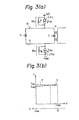
- Figure 3(a) is a circuit diagram of a conventional constant-current type battery feed circuit
- Fig. 3(b) is a graph depicting DC voltage-current characteristics of the subscriber lines A and B.
- the constant-current type battery feed circuit having the parts B and B b represents an improvement over the battery feed circuit of Fig. 2(a) in power consumption.
- the line A and line B side feed circuit parts B a and B b are basically constructed by pairs of resistors (R) and constant-current sources (CS), i.e., (R , CS ) and (R b , CS b ), respectively.
- the resistor (R) and the constant-current source (CS) are connected in parallel.
- FIG. 4 is more detailed circuit diagram of the battery feed circuit shown in Fig. 3(a).
- reference characters A O and A 1 denote operational amplifiers (hereinafter abbreviated as OP-AMP) and T r0 and T r1 denote transistors.
- Resistors R a0 , R b , and R a1 divide the voltage across the ground GD (OV) and the power source level (-VBB). The voltages across the resistors R a0 and R a1 are applied, as respective reference voltages, to the non-inverting input terminals (+) of the OP-AMP's A 0 and A 1 , respectively.
- the OP-AMP's operate so as to make the voltages across the resistors R eO and R e1 equal, respectively, to the voltages across the resistors R a0 and R al .
- the constant currents I sa and I sb flow through the respective resistors ReO and R e1 , which constant currents are defined as follows: Assuming here that the current amplification factor h FE satisfies h FE » 1, the constant current I sb along the resistor R e0 becomes substantially the same as the current flowing across the transistor T r0 . Similarly, the current I sa becomes the current flowing across the transistor T r1 .
- the resistors R O and R 1 preferably have neither too high nor too low resistance values. If the resistance values of the resistors R 0 and R 1 are too low, the constant-current characteristics are deteriorated and the transmission signal is attenuated thereby. Conversely, if they are too high, the constant-current characteristics are kept normal, but the intermediate voltage between the subscriber lines A and B is very liable to deviate from -V BB /2.
- the present invention proposes a battery feed circuit which features, first, iow power consumption with normal constant-current characteristics, second, superior noise suppression against common mode noise and/or power source noise, and, third, prevention of undesired clipping in the transmission signals through the subscriber lines A and B.
- FIG. 5 is a circuit diagram of a battery feed circuit for a subscriber line according to a first embodiment of the present invention.
- the differences here relative to the prior art construction shown in Fig. 4 are as follows. First, an intermediate voltage output circuit IV is newly employed. Second, a first reference voltage output circuit RV 0 and a second reference voltage output circuit RV 1 are newly employed, the related resistors R b0 and R b1 being equivalent to two identical resistors obtained by dividing R b shown in Fig. 4.
- the intermediate voltage output circuit IV operates to produce an intermediate voltage between the first and second subscriber lines A and B.
- the input of the amplifier A 2 is connected to an intermediate connecting point M1 of the resistors R c0 and R c1 , while the output of the amplifier A 2 is connected to an intermediate connecting point M 2 of the resistors R b0 and R bl .
- the amplifier A 2 is constructed as a voltage follower of gain 1 and is operative to feed the intermediate voltage at the point M 1 back to the intermediate point M 2 .
- usual transmission signals do not appear at the point M 1 since they form so-called differential mode signals between the lines A and B.
- the common mode signals at the output of the amplifier A 2 are applied to each non-inverting input terminal of the OP-AMP's A 0 and A l . Due to the inherent functions of the OP-AMP's A O and A 1 , the common mode signals appear at each inverting input terminal (-) of the OP-AMP's A 0 and A 1 .
- the common mode signals are then inverted by the transistors T r0 and T r1 , whereby the subscriber lines A and B are supplied with signals of opposite phases relative to the aforesaid common mode signals. Accordingly, the impedances of the first feed circuit part B b and second feed circuit part B a , in terms of the common mode signals, are reduced from infinity ( ⁇ ) to and respectively. Due to the reduction of the impedances, the common mode noise is cancelled by the feed circuit parts B b and B a . Therefore, the noise suppression capability for common mode noise is improved by the battery feed circuit of Fig. 5.
- the first embodiment can be further improved.
- the constant current concerned is determined merely by dividing the voltage between the ground (GD) level and the power source level -V BB . Accordingly, if a noise voltage V N is induced in the power source, the non-inverting input terminals of the OP-AMP's A 1 and A 0 are, respectively, supplied with the voltages V +1 and V +0 , which are expressed as follows: Consequently, the subscriber lines A and B are supplied with noise signals different from each other, which results in differential noise in the subscriber unit U.
- FIG. 6 is a circuit diagram of a battery feed circuit for a subscriber line according to a second embodiment of the present invention.
- the second embodiment improves the first embodiment with regard to the differential noise.
- the second embodiment differs from the construction of Fig. 5 in the provision of the following: a resistor R f0 connected between the emitter of the transistor T r0 and the inverting input terminal (-) of the OP-AMP A 0 ; a resistor R s0 and a DC-cut capacitor C o connected in series between the power source (-V BB ) and the inverting input terminal (-) of the OP-AMP A O ; a resistor R f1 connected between the emitter of the transistor T r1 and the inverting input terminal (-) of the OP-AMP A 1 ; and a resistor R s1 and a DC-cut capacitor C1 connected in series between the ground GD and the inverting input terminal (-) of the OP-AMP A l .
- the values of the resistors R f0 , R s0 , R f1 , and R s1 are determined to satisfy the following equations: and also, the values of the capacitors C 0 and C 1 are selected to be negligible impedances in terms of AC. Under these conditions, the non-inverting input terminal (+) of the OP-AMP A 1 is supplied with a voltage V +1 , due to the noise voltage V N , expressed as
- the voltage V -1 at the non-inverting input terminal of the OP-AMP A 1 assumes the following value due to the noise voltage V N :
- the battery feed circuit according the second embodiment is advantageous in that, even if power source noise is induced, differential noise resulting therefrom does not appear in the subscriber lines A and B.
- the second embodiment can be further improved, however.
- the OP-AMP's A O and A 1 continuously attempt to feed the constant currents even when the subscriber unit U is in an on-hook state, i.e., even when no loop current is needed. This is because the non-inverting input terminals of the OP-AMP's A 0 and A 1 are continuously supplied with voltages divided by the related resistors between the ground GD and the power source (-V BB ).
- the transistors T r0 and T r1 do not pass any current and accordingly, no voltage drop is induced across the resistors R e0 and R el . Accordingly, the 0 V level and -V BB level are given to the inverting input terminals (-) of the OP-AMP's A O and A 1 , respectively, which levels are not equal to the respective voltage V +0 and V +1 appearing at the non-inverting input terminals.
- the OP-AMP's thus function as comparators, the OP-AMP A 0 reducing its output voltage to the power source level -V BB .
- a constant current flows along the path of resistor R e0 ⁇ transistor T r0 ⁇ OP-AMP A 0 .
- the OP-AMP A 0 pulls as large a current, at its output terminal, as possible.
- Figure 7 is a circuit diagram of a battery feed circuit for a subscriber line according to a third embodiment of the present invention.
- the problem of the second embodiment of the uneconomical flow of current is improved.
- the difference relative to the construction of Fig. 6 lies in the provision of a resistor R dO for limiting current connected between the output terminal of the OP-AMP A 0 and the base of the transistor T r0 , a zener diode ZD 0 connected between the ground GD and the intermediate connecting point M 2 , a resistor R d1 for limiting current connected between the output terminal of the OP-AMP A 1 and the base of the transistor T r1 , a zener diode ZD 1 connected between the power source (-V BB ) and the intermediate connecting point M 2 , and a resistor R g connected between the point M 2 and the output terminal of the OP-AMP A 2 .
- the current during the on-hook state can be limited by the resistors R dO and R d1 . Accordingly, a low power consumption is attained.
- the resistors are selected to have a maximum resistance value in a range wherein sufficient base currents for the transistors T r0 and T r1 can be maintained during an off-hook state.
- the resistor R g and the zener diodes ZD 0 and ZD 1 are useful for emergencies such as ground-faults along the subscriber lines A and/or B or a faulty contact.
- an emergency such as ground-faults along the subscriber lines A and/or B or a faulty contact.
- the voltage at the intermediate connecting point M 1 becomes the ground (GD) level and the output of the OP-AMP A 2 changes to the ground (GD) level.
- GD ground
- the voltage level at the intermediate connecting point M l relative to the potential - V BB increases to twice the voltage normally obtained, and the constant current given from the feed circuit part B a increases two times the normal predetermined current.
- the power consumption increases four times the power normally consumed, necessitating reconsideration of heat design.
- the amplifier A 2 in each embodiment is not limited to a gain of 1 and may have a gain of over 1. If the gain G is higher than 1, the impedance in terms of the common mode noise induced in the subscriber lines A and B can advantageously be reduced by 1/ G . On the other hand, however, such an amplifier A 2 of a gain G (G > 1) cannot simply be fabricated, because a usual voltage follower cannot be used. Instead, a special non-inversion circuit is needed.
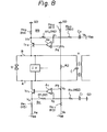
- Figure 8 is a circuit diagram for explaining the principle of a fourth embodiment.
- the construction of Fig. 8 is substantially the same as Figs. 6 and 7.
- the intermediate voltage output circuit IV is illustrated simply as a circuit block.
- the resistors R b0 and R b1 (including the zener diodes ZD 0 and ZD 1 ) are replaced by a single resistor having a resistance value of R 2 .
- Characters R1 through R 7 , R 81 and R 82 in parentheses denote respective resistance values.
- characters P a and Pb (in Fig. 10), and V 1 through V 4 are introduced for easy comprehension in relation to Fig. 9.
- Figure 9 depicts schematic diagrams of voltages appearing at major portions in Fig. 8.
- the voltage V 3 is preset as OV and the voltage V 4 is preset as a level equal to the power source noise voltage V N in order that the condition be satisfied that the voltage across the resistor of R 4 and the voltage across the resistor of R 5 be made OV. This is required for the following reason.
- the voltages appearing at the points P a and P b are defined as V 1 and V 2 , expressed below:
- the voltages V 1 and V 2 are applied to the non-inverting input terminals (+) of the OP-AMP's A 0 and A 1 , respectively.
- noise currents i nl and i n2 caused by the power source noise voltage V N flow through the resistors of R4 and R5 , respectively.
- the noise currents i n1 and i n2 are expressed as: Where, "0" denotes the ground (GD) level.
- the noise currents i n1 and i n2 cannot flow if no voltage is generated across each of the resistors (R4 and R5) by the power source noise voltage V N . This results in the aforesaid condition and, at the same time, is another way for proving the power source noise can be suppressed.
- the number of the resistors and capacitors is relatively large compared with the first embodiment of Fig. 5.
- the battery feed circuit according to the second and third embodiments can be improved in view of cost. Even a single reduction in the resistors and capacitors is beneficial for a switching system from the economical viewpoint, because battery feed circuits are allotted for every subscriber unit. If k subscribers are accommodated in the related switching system, up to k resistors and k capacitors, can be saved. Accordingly, the manufacturing cost may be reduced.
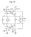
- FIG. 10 is a circuit diagram of a battery feed circuit according to the fourth embodiment of the present invention.
- the inverting input terminals (-) of the OP-AMP's A 0 and A 1 are connected to each other via both a resistor R S (resistance value of R8) and a capacitor C 01 connected in series.
- R S resistor
- FIG. 10 two electrical components are reduced compared with Fig. 8. Specifically, the four electrical components R S0 (R81), R S1 (R82), C 0 , and C 1 comprising the battery feed circuit of Fig. 8 are replaced in Fig. 10 by two electrical components R S (R8) and C 01 . This replacement may be made due to the following:
- the voltages V 1 and V 2 appearing at the points P a and P b in Fig. 10, are expressed by the previously recited equations, i.e.: Voltages identical to V 1 and V 2 also appear, due to "imaginary short-circuits", at the inverting input terminals of the OP-AMP's A 0 and A 1 . This being so, the aforesaid noise currents i n1 and i n2 flow through resistors of R4 and R5, respectively. In order to make these noise currents substantially zero, the voltages V 3 and V 4 are, preset respectively, to be OV and V N , as mentioned before.
- FIG 11 depicts schematic diagrams of voltages appearing at major portions in Fig. 10.
- the method of reading the diagrams is similar to that of Fig. 9.
- the difference with Fig. 9 is that the voltages V 1 and V 2 (refer to GD - V N in upper row of Fig. 9) are not used independently, as depicted in the middle row (V 3 - V N ) and in lower row (V 3 - V 4 ) of Fig. 9, but are commonly used, as depicted by V 3 - V 4 in the lower row of Fig. ll.
- the intended conditions i .e.
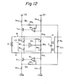
- FIG. 12 is a circuit diagram of a battery feed circuit according to a fifth embodiment of the present invention.
- the battery feed circuit of the fifth embodiment an improved version of the second embodiment and features a reduced number of electrical components.
- Figure 13 is a circuit diagram of a battery feed circuit according to a sixth embodiment of the present invention. This corresponds to a similar improved version of the third embodiment.
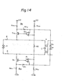
- FIG 14 is a circuit diagram of a battery feed circuit according to a seventh embodiment of the present invention.
- the battery feed circuit of the seventh embodiment excludes the intermediate voltage output circuit IV and its neighboring members. If the switching system is not expected to suffer from the aforesaid common mode noise but just the aforesaid power source noise, this embodiment is preferable from an economical viewpoint.
- the battery feed circuit according to the present invention is superior in view of one or more of power consumption, suppression of common mode noise, and suppression of power source noise.
Landscapes
- Engineering & Computer Science (AREA)
- Signal Processing (AREA)
- Power Engineering (AREA)
- Devices For Supply Of Signal Current (AREA)
- Interface Circuits In Exchanges (AREA)
Applications Claiming Priority (4)
| Application Number | Priority Date | Filing Date | Title |
|---|---|---|---|
| JP105660/84 | 1984-05-26 | ||
| JP59105660A JPS60250761A (ja) | 1984-05-26 | 1984-05-26 | 給電回路 |
| JP120668/84 | 1984-06-14 | ||
| JP59120668A JPS611160A (ja) | 1984-06-14 | 1984-06-14 | 加入者回路の定電流給電回路 |
Publications (4)
| Publication Number | Publication Date |
|---|---|
| EP0163275A2 true EP0163275A2 (fr) | 1985-12-04 |
| EP0163275A3 EP0163275A3 (en) | 1986-12-30 |
| EP0163275B1 EP0163275B1 (fr) | 1990-02-28 |
| EP0163275B2 EP0163275B2 (fr) | 1993-09-08 |
Family
ID=26445907
Family Applications (1)
| Application Number | Title | Priority Date | Filing Date |
|---|---|---|---|
| EP85106415A Expired - Lifetime EP0163275B2 (fr) | 1984-05-26 | 1985-05-24 | Circuit d'alimentation pour une ligne d'abonné |
Country Status (6)
| Country | Link |
|---|---|
| US (1) | US4631366A (fr) |
| EP (1) | EP0163275B2 (fr) |
| KR (1) | KR900000721B1 (fr) |
| AU (1) | AU560001B2 (fr) |
| CA (1) | CA1233580A (fr) |
| DE (1) | DE3576266D1 (fr) |
Cited By (3)
| Publication number | Priority date | Publication date | Assignee | Title |
|---|---|---|---|---|
| US4926473A (en) * | 1987-08-25 | 1990-05-15 | Rockwell International Corporation | Longitudinal balance system |
| GB2224909A (en) * | 1988-11-11 | 1990-05-16 | Stc Plc | Balanced constant current feed for subscriber lines |
| US5172412A (en) * | 1989-08-15 | 1992-12-15 | Oki Electric Industry Co., Ltd. | Subscriber circuit capable of suppressing in-phase induced noise |
Families Citing this family (6)
| Publication number | Priority date | Publication date | Assignee | Title |
|---|---|---|---|---|
| DE3428106A1 (de) * | 1984-07-30 | 1986-02-06 | Standard Elektrik Lorenz Ag, 7000 Stuttgart | Teilnehmeranschlussschaltung |
| CA1333189C (fr) * | 1987-06-17 | 1994-11-22 | Toshiro Tojo | Circuit de protection pour circuit d'alimentation de batterie |
| CA1291836C (fr) * | 1987-06-17 | 1991-11-05 | Kenji Takato | Circuit d'alimentation pour accumulateur |
| JP3322889B2 (ja) * | 1991-03-19 | 2002-09-09 | 株式会社東芝 | 給電伝送システム |
| US6621904B1 (en) * | 1999-09-29 | 2003-09-16 | Agere Systems Inc. | Pre-charging line modem capacitors to reduce DC setup time |
| US7130414B2 (en) * | 2002-03-04 | 2006-10-31 | Intersil Americas Inc. | Active mode line voltage regulator for ringing subscriber line interface circuit |
Family Cites Families (8)
| Publication number | Priority date | Publication date | Assignee | Title |
|---|---|---|---|---|
| IT7823635A0 (it) * | 1978-05-22 | 1978-05-22 | Sits Soc It Telecom Siemens | Di commutazione. ponte di alimentazione a corrente costante per centrali telefoniche |
| DE2835526C2 (de) * | 1978-08-14 | 1982-09-09 | Siemens AG, 1000 Berlin und 8000 München | Verfahren zur spulen-, relaiskontakt- und transformatorfreien Rufstrom- und Schleifenstromeinspeisung |
| DE2850905C2 (de) * | 1978-11-24 | 1985-11-14 | Felten & Guilleaume Fernmeldeanlagen GmbH, 8500 Nürnberg | Schaltungsanordnung zur Speisung einer Teilnehmerendeinrichtung |
| DE3037972C2 (de) * | 1980-10-08 | 1982-09-16 | Standard Elektrik Lorenz Ag, 7000 Stuttgart | Schaltungsanordnung zum Speisen eines veränderlichen Widerstandes über zwei veränderliche Speisewiderstände, insbesondere zum Speisen von Teilnehmeranschlußleitungen in Fernsprechvermittlungsanlagen |
| DE3116783C2 (de) * | 1981-04-28 | 1983-09-01 | Standard Elektrik Lorenz Ag, 7000 Stuttgart | Schaltungsanordnung für eine Teilnehmeranschlußschaltung für Fernsprechanlagen |
| DE3138649A1 (de) * | 1981-09-29 | 1983-04-14 | TE KA DE Felten & Guilleaume Fernmeldeanlagen GmbH, 8500 Nürnberg | Verfahren und schaltungsanordnung zur speisung einer teilnehmerendeinrichtung |
| SE433285B (sv) * | 1982-09-22 | 1984-05-14 | Ericsson Telefon Ab L M | Anordning for strommatning av en abonnentapparat |
| US4567331A (en) * | 1983-12-22 | 1986-01-28 | Itt Corporation | Electronic hybrid having synthesized impedance circuitry |
-
1985
- 1985-05-17 CA CA000481865A patent/CA1233580A/fr not_active Expired
- 1985-05-21 US US06/736,345 patent/US4631366A/en not_active Expired - Fee Related
- 1985-05-23 KR KR1019850003559A patent/KR900000721B1/ko not_active Expired
- 1985-05-24 DE DE8585106415T patent/DE3576266D1/de not_active Expired - Lifetime
- 1985-05-24 EP EP85106415A patent/EP0163275B2/fr not_active Expired - Lifetime
- 1985-05-24 AU AU42834/85A patent/AU560001B2/en not_active Ceased
Cited By (3)
| Publication number | Priority date | Publication date | Assignee | Title |
|---|---|---|---|---|
| US4926473A (en) * | 1987-08-25 | 1990-05-15 | Rockwell International Corporation | Longitudinal balance system |
| GB2224909A (en) * | 1988-11-11 | 1990-05-16 | Stc Plc | Balanced constant current feed for subscriber lines |
| US5172412A (en) * | 1989-08-15 | 1992-12-15 | Oki Electric Industry Co., Ltd. | Subscriber circuit capable of suppressing in-phase induced noise |
Also Published As
| Publication number | Publication date |
|---|---|
| DE3576266D1 (de) | 1990-04-05 |
| EP0163275B2 (fr) | 1993-09-08 |
| AU4283485A (en) | 1985-11-28 |
| KR850008590A (ko) | 1985-12-18 |
| AU560001B2 (en) | 1987-03-26 |
| EP0163275B1 (fr) | 1990-02-28 |
| US4631366A (en) | 1986-12-23 |
| CA1233580A (fr) | 1988-03-01 |
| EP0163275A3 (en) | 1986-12-30 |
| KR900000721B1 (ko) | 1990-02-07 |
Similar Documents
| Publication | Publication Date | Title |
|---|---|---|
| US4827505A (en) | Subscriber line interface circuit | |
| CA1084185A (fr) | Circuit hybride a deux fils/quatre fils sans transformateur avec possibilite d'alimentation en continu | |
| PL125418B1 (en) | Microprocessor controlled telephone transmission system | |
| US4203009A (en) | Unbalanced/balanced converter circuits | |
| EP0163275B1 (fr) | Circuit d'alimentation pour une ligne d'abonné | |
| US4319093A (en) | Transmission bridge for a subscriber set | |
| JPH0626400B2 (ja) | 電話システム用電子バツテリーフイード回路 | |
| US4027235A (en) | Direct current compensation circuit with current threshold detection | |
| CN1132433A (zh) | 带降噪电路的电话电池供电电路 | |
| US5444777A (en) | Battery feed for telephone line cards | |
| KR900001340B1 (ko) | 한쌍의 가입자선용 밧데리 피이드 회로 | |
| US4243842A (en) | Telephone line circuit | |
| US3083265A (en) | Conference call circuit | |
| US4297531A (en) | Circuit for suppressing noise influences in the evaluation of signal states on transmission lines | |
| EP0096473B1 (fr) | Circuit d'alimentation de ligne à impédance active | |
| US4588860A (en) | Battery feed circuit for telephone subscriber line | |
| CA1157978A (fr) | Circuit de detection de boucle pour circuit d'interface de boucle d'abonne | |
| US4454477A (en) | Loop current detector with threshold setting impedance | |
| US4734937A (en) | Telephone installation | |
| JP2912388B2 (ja) | 加入者回路 | |
| CA1114972A (fr) | Circuit de ligne telephonique | |
| CA1074034A (fr) | Circuit de ligne telephonique avec detection de courant de boucle differentiel et compensation | |
| CA2193154C (fr) | Circuit et methode pour reduire le brouillage en mode commun dans les appareils telephoniques | |
| US3300588A (en) | Line circuits for subscribers' telephones | |
| JPS611160A (ja) | 加入者回路の定電流給電回路 |
Legal Events
| Date | Code | Title | Description |
|---|---|---|---|
| PUAI | Public reference made under article 153(3) epc to a published international application that has entered the european phase |
Free format text: ORIGINAL CODE: 0009012 |
|
| AK | Designated contracting states |
Designated state(s): BE DE FR GB |
|
| PUAL | Search report despatched |
Free format text: ORIGINAL CODE: 0009013 |
|
| AK | Designated contracting states |
Kind code of ref document: A3 Designated state(s): BE DE FR GB |
|
| 17P | Request for examination filed |
Effective date: 19870212 |
|
| 17Q | First examination report despatched |
Effective date: 19880929 |
|
| GRAA | (expected) grant |
Free format text: ORIGINAL CODE: 0009210 |
|
| AK | Designated contracting states |
Kind code of ref document: B1 Designated state(s): BE DE FR GB |
|
| ET | Fr: translation filed | ||
| REF | Corresponds to: |
Ref document number: 3576266 Country of ref document: DE Date of ref document: 19900405 |
|
| PLBI | Opposition filed |
Free format text: ORIGINAL CODE: 0009260 |
|
| 26 | Opposition filed |
Opponent name: PHILIPS PATENTVERWALTUNG GMBH Effective date: 19901115 |
|
| PGFP | Annual fee paid to national office [announced via postgrant information from national office to epo] |
Ref country code: GB Payment date: 19930309 Year of fee payment: 9 |
|
| PGFP | Annual fee paid to national office [announced via postgrant information from national office to epo] |
Ref country code: BE Payment date: 19930326 Year of fee payment: 9 |
|
| PGFP | Annual fee paid to national office [announced via postgrant information from national office to epo] |
Ref country code: FR Payment date: 19930526 Year of fee payment: 9 |
|
| PGFP | Annual fee paid to national office [announced via postgrant information from national office to epo] |
Ref country code: DE Payment date: 19930714 Year of fee payment: 9 |
|
| PUAH | Patent maintained in amended form |
Free format text: ORIGINAL CODE: 0009272 |
|
| STAA | Information on the status of an ep patent application or granted ep patent |
Free format text: STATUS: PATENT MAINTAINED AS AMENDED |
|
| 27A | Patent maintained in amended form |
Effective date: 19930908 |
|
| AK | Designated contracting states |
Kind code of ref document: B2 Designated state(s): BE DE FR GB |
|
| ET3 | Fr: translation filed ** decision concerning opposition | ||
| PG25 | Lapsed in a contracting state [announced via postgrant information from national office to epo] |
Ref country code: GB Effective date: 19940524 |
|
| PG25 | Lapsed in a contracting state [announced via postgrant information from national office to epo] |
Ref country code: BE Effective date: 19940531 |
|
| BERE | Be: lapsed |
Owner name: FUJITSU LTD Effective date: 19940531 |
|
| GBPC | Gb: european patent ceased through non-payment of renewal fee |
Effective date: 19940524 |
|
| PG25 | Lapsed in a contracting state [announced via postgrant information from national office to epo] |
Ref country code: FR Effective date: 19950131 |
|
| PG25 | Lapsed in a contracting state [announced via postgrant information from national office to epo] |
Ref country code: DE Effective date: 19950201 |
|
| REG | Reference to a national code |
Ref country code: FR Ref legal event code: ST |