EP0164209A1 - Dispositif de test pour circuit intégré - Google Patents
Dispositif de test pour circuit intégré Download PDFInfo
- Publication number
- EP0164209A1 EP0164209A1 EP85302946A EP85302946A EP0164209A1 EP 0164209 A1 EP0164209 A1 EP 0164209A1 EP 85302946 A EP85302946 A EP 85302946A EP 85302946 A EP85302946 A EP 85302946A EP 0164209 A1 EP0164209 A1 EP 0164209A1
- Authority
- EP
- European Patent Office
- Prior art keywords
- scan path
- lfsr
- output
- arrangement
- combinational logic
- Prior art date
- Legal status (The legal status is an assumption and is not a legal conclusion. Google has not performed a legal analysis and makes no representation as to the accuracy of the status listed.)
- Withdrawn
Links
Images


Classifications
-
- G—PHYSICS
- G06—COMPUTING OR CALCULATING; COUNTING
- G06F—ELECTRIC DIGITAL DATA PROCESSING
- G06F11/00—Error detection; Error correction; Monitoring
- G06F11/22—Detection or location of defective computer hardware by testing during standby operation or during idle time, e.g. start-up testing
- G06F11/26—Functional testing
- G06F11/27—Built-in tests
Definitions
- This invention relates to integrated circuit testing arrangements.
- LSSD level sensitive scan design
- the circuit is designed so as to comprise a number of bistable elements e.g. D-type flip-flops, which for test purposes are connected in series to form effectively a shift register known as a scan path. Apart from these bistable elements the circuit elements are all logic elements which together form a combinational logic arrangement whose required response to known inputs is totally predictable.
- the test technique involves deriving inputs for the combinational logic from the scan path and monitoring the resulting outputs of the combinational logic. To test the circuit sequences of data are successively entered into the scan path shift register from a test generator, and the outputs of the combinational logic monitored for each such sequence.
- the scan path elements are first set to predetermined states by a data sequence derived from the test generator.
- the resulting outputs of the scan path elements are applied to the inputs of the combinational logic and the scan path elements reset in accordance with the resulting outputs of the combinational logic.
- the resulting data in the scan path is then shifted out to an analyser, normally referred to as a signature analyser, to determine whether the circuit operated correctly.
- the test cycle is then repeated with a new sequence of data entered into the scan path as the test result data was shifted out.
- test sequence generator is arranged to generate pseudo random data sequences for entry to the scan path.
- combinational logic is not exhaustively tested, i.e. the combinational logic is not tested under every different possible combination of inputs.
- the scan path is divided into two parts, one part being used to set the inputs to the combinational logic and the other part being used to monitor the outputs of the combinational logic.
- the test data sequence in the part of the scan path connected to the inputs of the combinational logic is not lost when reading out data and it is possible to generate successive sequences of data for testing by shifting the data in the input path of the scan path in steps across the inputs of the combinational logic.
- the design rules requirement to connect some of the scan path elements solely to inputs of the combinational logic and others of the scan path elements solely to outputs of the combinational logic renders circuit design a practical impossibility.
- an integrated circuit testing arrangement comprises: a scan path comprising bistable elements of the integrated circuit connected, for testing purposes, in a series shift register arrangement, the elements of the scan path each having an output connected to an input of a combinational logic arrangement of the integrated circuit and an input connected to an output of said combinational logic arrangement; a test sequence generator for supplying binary data for clocking into the scan path for test purposes, the generator being arranged to supply sequences of data to the scan path each having a number of bits equal to the number of elements in the scan path; means for clocking the elements of the scan path to cause each element to assume either the same state as the preceding element in the scan path, or to assume the state of the associated output of the combinational logic arrangement, the clocking means being operable to cause alternately the scan path elements to assume the states of the associated outputs of the combinational logic arrangement, and to receive a new sequence of data from said test generator; and means for analysing data clocked out of said scan path as each new sequence of data is received from said generator; said generator being arranged to
- said test generator comprises an N-stage linear feed back shift register (LFSR) having an output which is supplied to an input of the first element in the scan path, the LFSR being clocked through its possible states to effect insertion of each new sequence of data into the scan path, the LFSR having 2 N -1 different possible states, and the number of different possible states and the number of elements in the scan path being realtively prime.
- LFSR linear feed back shift register
- Two (or more) numbers are said to be relatively prime when their greatest common divider is one.
- an LFSR is meant an arrangement comprising a recirculating shift register modified so that, on being clocked, at least one stage assumes a state determined by a linear combination of the state of the preceding stage and at least one other stage.
- the output of an LFSR is derived from a single stage, but an output may alternatively or additionally be constituted by a linear combination of the states of any two or more stages of the register.
- the LFSR in order to achieve exhaustive testing, the LFSR must of course still be chosen so as to meet the requirementaccording to the invention regarding each set of inputs of the combinational logic arrangement which are connected via the combinational logic to the same output of the logic.
- the choice of a suitable LFSR for testing a particular integrated circuit arrangement is a relatively simple matter using a computer.
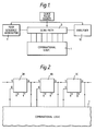
- the integrated circuit to be tested is designed so as to comprise a large arrangement 1 of combinational logic elements, i.e. gates, each of which elements produces a predictable desired output in response to any combination of possible inputs.
- the circuit includes a number of bistable elements,each of the bistable elements comprising a D-type flip-flop 3. It will be understood that for testing purposes the operation of the circuit as a whole with each flip-flop 3 in either one of its two possible states must be considered. In the case of the logic elements no such comparable consideration exists.
- each flip-flop 3 in the scan path has an output Q which is connected to a point in the combinational logic arrangement 1 and to a first input S of the succeeding flip-flop in the scan path.
- each flip-flop 3 has a second input D which is connected to a point in the combinational logic arrangement 1.
- each flip-flop 3 has two clocking inputs X and Y clock pulses applied to which respectively cause the output Q to assume the same binary state (0 or 1) as the S or D input.
- the first flip-flop 3 in the scan path has its S input connected to the output of a test sequence generator 7, further described below.
- the last flip-flop 3 in the scan path has its output Q connected to the input of a signature analyser 9 further described below.
- each flip-flop 3 has both an input and an output connected to the computational logic arrangement, some flip-flops may have only an input or an output so connected.
- further flip-flops may be included in the scan path 5 which serve no function in the integrated circuit per se, and are provided only for test purposes, e.g. to provide or receive a signal which in operation of the integrated circuit is derived from a point external of the integrated circuit.
- clock pulses are supplied from a source 10 to the generator 7 and the flip-flops 3 in the scan path to cause the test sequence generator 7 to supply a sequence of bits to the scan path 5 equal to the number of flip-flops 3 in the scan path 5, clock pulses being applied to the X clocking input of the flip-flops for this purpose.
- the Q output of each of the flip-flops 3 in the scan path 5 consequently assumes a state determined by a different one of the sequence of bits fed to the scan path 5 by the test generator 7.
- the signals at the D inputs of the flip-flops 3 take up states dependent on the design and configuration of the combinational logic arrangement.
- a clock pulse is then applied simultaneously to the Y clocking input of all the flip-flops 3 causing the flip-flops 3 to take up the states of the signals at their D inputs.
- the analyser 9 comprises any suitable means for determining whether the sequences fed to it from the scan path 5 are correct.
- the analyser typically comprises some means of compacting the sequences of bits fed to it such as an LFSR and comparing the compacted data or signature with a computed correct signature.
- the sequences of bits supplied to the scan path 5 by the generator 7 must be such that for each so-called cone of the combinational logic arrangement 1, all possible combinations of inputs are applied to the inputs of the cone.
- the cones present in the integrated circuit are identified by considering each output from the combinational logic 1 to the scan path 5, and identifying the inputs to the combinational logic 1 from the scan path 5 which are connected with, and whose states may therefore effect, the state of that output.
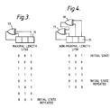
- the test generator 7 comprises a linear feedback shift register (LFSR) of maximal length, that is to say an LFSR arranged so that when clocked it cycles through 2 N - 1 different states before returning to its initial state, N being the number of stages in the LFSR.
- LFSR linear feedback shift register
- N the number of stages in the LFSR.
- this LFSR comprises a 3-stage shift register 11 whose first stage is set on clocking to the state of the output of an exclusive OR gate 13 whose inputs are derived from the first and third stages of the register 11.
- Figure 4 shows a non-maximal length LFSR comprising a three-stage shift register 15 whose first stage is set on clocking to the output of an exclusive OR gate 17 whose inputs are derived from the first stage of the LFSR register 15 and the output of a further exclusive OR gate 19 whose inputs are derived from the secondhand third stages of the LFSR register 15.
- the generator 7 comprises an LFSR chosen so that the number of different possible states 2 N - 1 which it has and the number of stages i.e. flip-flops 3 in the scan path 5 are relatively prime.
- Figure 5 shows the LFSR 11, 13 of Figure 3 the state of whose final stage constitutes the input of a six stage scan path 21, the stages of the scan path 21 being referenced A to F respectively. Since the LFSR 11, 13 has seven (2 J -1) possible different states and the scan path 21 has six stages and the greatest common divisor of six and seven is one the LFSR and scan path are of the required relative form. In operation of the arrangement, the LFSR 11, 13 is clocked six times to insert each new sequence of data into the scan path 21. In Figure 4 all the possible sequences of data are shown on the right under the scan path 21, and the state of the LFSR 11, 13 prior to clocking in each new sequence is shown on the left under the LFSR.
- each set of three consecutive stages of the scan path cycles through all seven of the possible states of the LFSR 11, 13.
- an LFSR 23 and scan path 25 not of the required relative form are shown in Figure 6.
- the LFSR 23 comprises a four stage shift register 27 whose first stage is set on clocking to the state of the output of an exclusive OR gate 29 whose inputs are derived from the first and fourth stages of the register 27.
- this arrangement is of maximal length and therefore has fifteen (2"-1) different possible states.
- the scan path 25 has six stages so that the number of stages in the scan path and the number of different possible states of the LFSR 23 are not relatively prime.
- the test sequence inserted into the scan path 25 repeat after three sequences and no set of two or more stages of the scan path 25 cycles through all its possible different states.
- the scan path 5 will have a much larger number of stages than is shown in Figures 5 or 6. Consequently, the time taken to insert new sequences into the scan path from the LFSR test generator 7 is a large fraction of the total test time.
- the scan path 5 may be partitioned into two or more sections of equal length fed from the LFSR test generator 7 in parallel.
- each section is fed with the same sequence from the test generator 7,
- Figure 7 illustrating one such arrangement wherein two seven stage scan path sections 31 and 33 are fed from an LFSR 35.
- the same sequence of states occurs in corresponding stages of each section, i.e. stage Ax of section 31 and stage Bx of section 33, where x is the number of the stage.
- This difficulty can be overcome by choosing an LFSR having a number of possible different stages equal to or greater than the total number of stages in the scan path, and arranging for each stage of each section of the scan path to receive a uniquely phase shifted version of the sequence of bits produced by the LFSR. It is pointed out in this connection that an LFSR having P different states produces in each and every stage of itself and hence of the scan path a repeating sequence of P bits. This sequence is phase shifted by one bit from stage to stage of the LFSR and by one bit from stage to stage of each section of the-scan path.
- an LFSR having a four stage shift register 37 whose first stage is set on clocking to the state of the output of an exclusive OR gate 39 whose inputs are derived from the first and fourth stages of the register 37.
- the scan path comprises two sections 41 and 43 each having seven stages A1 to A7 or B1 to B7.
- the scan path section 41 is fed from the final stage of the LFSR register 37, the sequences of bits appearing in the section being as shown in Figure 8 starting with an initial state 0001 in the register 37.
- the other scan path section 43 is fed from the output an exclusive OR gate, 45 whose inputs are derived from the third stage of the LFSR register 29 and the output of a further exclusive OR gate 47 whose inputs are derived from the first and second stages of the LFSR register 37.
- the sequences produced in the scan path section 43 are shown in Figure 8.
- the LFSR 37 produces a repeating sequence of fifteen bits and that the sequence fed to section 41 of the scan path lags the sequence fed to section 43 by seven bits. Hence each stage of both sections 41 and 43 of the scan path receives a uniquely phase shifted version of the LFSR sequence.
- the LFSR 51 comprises N serially connected flip-flop stages 51A to 51N, the first stage 51A of which is set on clocking to the state of an exclusive OR gate 53 whose inputs are derived from appropriate ones of the other stages such that the LFSR is of maximal length.
- the output of the final stage 51N is fed to one input of a multiplexer 55, and the other inputs of the multiplexer are fed from the outputs of respective ones of a number of exclusive OR gates 57A, 57B, 57C.
- the inputs of the exclusive OR gates 57A etc. are derived from the outputs of selected ones of the stages of the LFSR 51 so that the signals applied to the inputs of the multiplexer are all differently phase shifted versions of the same basic sequence.
- Figure 10 shows an exclusive OR gate 61 whose inputs are derived from the last two stages of a four stage maximal length LFSR 63 to produce at its output the same sequence as appears at the output of the LFSR but lagging the LFSR sequence by three bits.
- the multiplexer 55 is controlled by a counter 59 in response to the clocking pulses applied to the LFSR 51 so that at the output of the multiplexer 55 the four inputs to the multiplexer appear in the sequence A1, B1, C1, D1, A2, B2, C2, D2, A3 etc.
- A1, A2 etc. is the sequence at the output of the LFSR 51 and A2, B2 etc.
- A3, B3 etc. and A4, B4 etc. are the sequences at the outputs of gates 57A, 57B and 57C respectively.
- the output of the multiplexer 55 which is applied to the scan path (not shown) comprises an interleaving of the various phase shifted versions of the sequence produced by the LFSR 51.
- test generator and analyser are suitably fabricated on the same semiconductor chip as the integrated circuit per se.
- the remaining parts of the testing arrangement such as a clock pulse generator and automatic test control equipment to enable the circuit to effect self testing may also be incorporated on the same chip, or alternatively may be fabricated on a second chip, or in any other separate form.
Landscapes
- Engineering & Computer Science (AREA)
- General Engineering & Computer Science (AREA)
- Theoretical Computer Science (AREA)
- Computer Hardware Design (AREA)
- Quality & Reliability (AREA)
- Physics & Mathematics (AREA)
- General Physics & Mathematics (AREA)
- Tests Of Electronic Circuits (AREA)
Applications Claiming Priority (2)
| Application Number | Priority Date | Filing Date | Title |
|---|---|---|---|
| GB848411733A GB8411733D0 (en) | 1984-05-09 | 1984-05-09 | Integrated circuit testing arrangements |
| GB8411733 | 1984-05-09 |
Publications (1)
| Publication Number | Publication Date |
|---|---|
| EP0164209A1 true EP0164209A1 (fr) | 1985-12-11 |
Family
ID=10560638
Family Applications (1)
| Application Number | Title | Priority Date | Filing Date |
|---|---|---|---|
| EP85302946A Withdrawn EP0164209A1 (fr) | 1984-05-09 | 1985-04-26 | Dispositif de test pour circuit intégré |
Country Status (3)
| Country | Link |
|---|---|
| EP (1) | EP0164209A1 (fr) |
| JP (1) | JPS60253985A (fr) |
| GB (2) | GB8411733D0 (fr) |
Cited By (6)
| Publication number | Priority date | Publication date | Assignee | Title |
|---|---|---|---|---|
| EP0266874A3 (en) * | 1986-11-06 | 1990-06-13 | International Computers Limited | Testing programmable logic arrays |
| EP0408299A3 (en) * | 1989-07-11 | 1992-03-18 | Fujitsu Limited | Semiconductor integrated circuit device and test method therefor |
| EP0444806A3 (en) * | 1990-02-26 | 1992-07-22 | American Telephone And Telegraph Company | Pseudo-exhaustive self-test technique |
| EP0498191A1 (fr) * | 1991-02-04 | 1992-08-12 | International Business Machines Corporation | Couverture de test de retard d'un circuit logique utilisant le concept du balayage sensible aux niveaux |
| EP0549949A3 (en) * | 1991-12-16 | 1994-06-15 | Nippon Telegraph & Telephone | Built-in self test circuit |
| US6768292B2 (en) * | 2001-03-07 | 2004-07-27 | Koninklijke Philips Electronics N.V. | Arrangement and method having a data word generator for testing integrated circuits |
Families Citing this family (4)
| Publication number | Priority date | Publication date | Assignee | Title |
|---|---|---|---|---|
| GB8826921D0 (en) * | 1988-11-17 | 1988-12-21 | Datatrace Ltd | Circuit testing |
| US5608897A (en) * | 1994-04-05 | 1997-03-04 | International Business Machines Corporation | Programmable linear feedback shift register timeout mechanism |
| RU2179729C2 (ru) * | 2000-02-25 | 2002-02-20 | Пюкке Георгий Александрович | Устройство для проверки электронных схем |
| RU2196340C2 (ru) * | 2001-02-19 | 2003-01-10 | Пюкке Георгий Александрович | Устройство регулярно-периодического контроля работоспособности электрических средств автоматизации |
Citations (1)
| Publication number | Priority date | Publication date | Assignee | Title |
|---|---|---|---|---|
| US3790885A (en) * | 1972-03-27 | 1974-02-05 | Ibm | Serial test patterns for mosfet testing |
-
1984
- 1984-05-09 GB GB848411733A patent/GB8411733D0/en active Pending
-
1985
- 1985-04-24 GB GB08510439A patent/GB2159287B/en not_active Expired
- 1985-04-26 EP EP85302946A patent/EP0164209A1/fr not_active Withdrawn
- 1985-05-08 JP JP60097680A patent/JPS60253985A/ja active Pending
Patent Citations (1)
| Publication number | Priority date | Publication date | Assignee | Title |
|---|---|---|---|---|
| US3790885A (en) * | 1972-03-27 | 1974-02-05 | Ibm | Serial test patterns for mosfet testing |
Non-Patent Citations (2)
| Title |
|---|
| IBM JOURNAL OF RESEARCH AND DEVELOPMENT, vol. 27, no. 3, May 1983, pages 265-272, New York, US; E.B. EICHELBERGER: "Random-pattern coverage enhancement and diagnosis for LSSD logic self-test" * |
| IEEE TRANSACTIONS ON COMPUTERS, vol. C-31, no. 1, January 1982, pages 2-15, IEEE, New York, US; T.W. WILLIAMS et al.: "Design for testability - a survey" * |
Cited By (8)
| Publication number | Priority date | Publication date | Assignee | Title |
|---|---|---|---|---|
| EP0266874A3 (en) * | 1986-11-06 | 1990-06-13 | International Computers Limited | Testing programmable logic arrays |
| EP0408299A3 (en) * | 1989-07-11 | 1992-03-18 | Fujitsu Limited | Semiconductor integrated circuit device and test method therefor |
| US5341096A (en) * | 1989-07-11 | 1994-08-23 | Fujitsu Limited | Semiconductor integrated circuit having a scan circuit provided with a self-contained signal generator circuit |
| EP0444806A3 (en) * | 1990-02-26 | 1992-07-22 | American Telephone And Telegraph Company | Pseudo-exhaustive self-test technique |
| US5457697A (en) * | 1990-02-26 | 1995-10-10 | At&T Ipm Corp. | Pseudo-exhaustive self-test technique |
| EP0498191A1 (fr) * | 1991-02-04 | 1992-08-12 | International Business Machines Corporation | Couverture de test de retard d'un circuit logique utilisant le concept du balayage sensible aux niveaux |
| EP0549949A3 (en) * | 1991-12-16 | 1994-06-15 | Nippon Telegraph & Telephone | Built-in self test circuit |
| US6768292B2 (en) * | 2001-03-07 | 2004-07-27 | Koninklijke Philips Electronics N.V. | Arrangement and method having a data word generator for testing integrated circuits |
Also Published As
| Publication number | Publication date |
|---|---|
| JPS60253985A (ja) | 1985-12-14 |
| GB2159287A (en) | 1985-11-27 |
| GB8411733D0 (en) | 1984-06-13 |
| GB2159287B (en) | 1988-01-13 |
| GB8510439D0 (en) | 1985-05-30 |
Similar Documents
| Publication | Publication Date | Title |
|---|---|---|
| US5258986A (en) | Tightly coupled, low overhead RAM built-in self-test logic with particular applications for embedded memories | |
| US4974184A (en) | Maximum length pseudo-random test pattern generator via feedback network modification | |
| EP0196171B1 (fr) | Circuits numériques intégrés | |
| US4340857A (en) | Device for testing digital circuits using built-in logic block observers (BILBO's) | |
| EP0023972B1 (fr) | Système d'unités fonctionnelles pour la réalisation de fonctions logiques | |
| US7836368B2 (en) | Dynamically reconfigurable shared scan-in test architecture | |
| US3783254A (en) | Level sensitive logic system | |
| EP0190494B1 (fr) | Montage pour un circuit intégré comprenant un dispositif d'autocontrôle | |
| EP0195164A1 (fr) | Circuits intégrés | |
| EP0358376A2 (fr) | Circuit de test intégré | |
| JPH02195281A (ja) | 擬似ランダム・パターン生成機構及び位相シフトを増加させる方法 | |
| GB1581865A (en) | Method of testing a logic system | |
| US4847839A (en) | Digital registers with serial accessed mode control bit | |
| EP0319187B1 (fr) | Couplage de chemin de données de test | |
| EP0289158B1 (fr) | Appareil de diagnostic pour un système de traitement de données | |
| EP0164209A1 (fr) | Dispositif de test pour circuit intégré | |
| US7430698B2 (en) | Method and system for an on-chip AC self-test controller | |
| EP0318140A2 (fr) | Générateur pseudo-aléatoire et circuit de somme de vérification pour puce VLSI | |
| EP0209982B1 (fr) | Circuits intégrés numériques | |
| US5029171A (en) | Test vector generation system | |
| KR940011036B1 (ko) | 시프트 레지스터 | |
| US5473651A (en) | Method and apparatus for testing large embedded counters | |
| EP0650123A1 (fr) | Circuit logique intégré avec trajet d'analyse | |
| US20070168798A1 (en) | Scan string segmentation for digital test compression | |
| US5694444A (en) | Testable high count counter |
Legal Events
| Date | Code | Title | Description |
|---|---|---|---|
| PUAI | Public reference made under article 153(3) epc to a published international application that has entered the european phase |
Free format text: ORIGINAL CODE: 0009012 |
|
| AK | Designated contracting states |
Designated state(s): DE FR IT NL |
|
| 17P | Request for examination filed |
Effective date: 19860609 |
|
| 17Q | First examination report despatched |
Effective date: 19880314 |
|
| STAA | Information on the status of an ep patent application or granted ep patent |
Free format text: STATUS: THE APPLICATION IS DEEMED TO BE WITHDRAWN |
|
| 18D | Application deemed to be withdrawn |
Effective date: 19890718 |
|
| RIN1 | Information on inventor provided before grant (corrected) |
Inventor name: BAKER, KEITH |