EP0164806B1 - Circuit PLL - Google Patents
Circuit PLL Download PDFInfo
- Publication number
- EP0164806B1 EP0164806B1 EP19850200903 EP85200903A EP0164806B1 EP 0164806 B1 EP0164806 B1 EP 0164806B1 EP 19850200903 EP19850200903 EP 19850200903 EP 85200903 A EP85200903 A EP 85200903A EP 0164806 B1 EP0164806 B1 EP 0164806B1
- Authority
- EP
- European Patent Office
- Prior art keywords
- input
- flip flop
- output
- signal
- frequency
- Prior art date
- Legal status (The legal status is an assumption and is not a legal conclusion. Google has not performed a legal analysis and makes no representation as to the accuracy of the status listed.)
- Expired
Links
- 230000007704 transition Effects 0.000 claims description 6
- 230000001960 triggered effect Effects 0.000 claims description 4
- 230000003213 activating effect Effects 0.000 claims 3
- 230000000295 complement effect Effects 0.000 claims 2
- 230000004913 activation Effects 0.000 claims 1
- 230000000630 rising effect Effects 0.000 description 9
- 230000000694 effects Effects 0.000 description 4
- PEDCQBHIVMGVHV-UHFFFAOYSA-N Glycerine Chemical compound OCC(O)CO PEDCQBHIVMGVHV-UHFFFAOYSA-N 0.000 description 2
- 239000003990 capacitor Substances 0.000 description 2
- 238000010586 diagram Methods 0.000 description 2
- 238000000605 extraction Methods 0.000 description 2
- 230000001419 dependent effect Effects 0.000 description 1
- 238000001514 detection method Methods 0.000 description 1
- 230000006870 function Effects 0.000 description 1
- 238000000034 method Methods 0.000 description 1
- 230000010363 phase shift Effects 0.000 description 1
- 230000002035 prolonged effect Effects 0.000 description 1
- 238000011084 recovery Methods 0.000 description 1
Images

Classifications
-
- H—ELECTRICITY
- H03—ELECTRONIC CIRCUITRY
- H03L—AUTOMATIC CONTROL, STARTING, SYNCHRONISATION OR STABILISATION OF GENERATORS OF ELECTRONIC OSCILLATIONS OR PULSES
- H03L7/00—Automatic control of frequency or phase; Synchronisation
- H03L7/06—Automatic control of frequency or phase; Synchronisation using a reference signal applied to a frequency- or phase-locked loop
- H03L7/08—Details of the phase-locked loop
- H03L7/10—Details of the phase-locked loop for assuring initial synchronisation or for broadening the capture range
- H03L7/113—Details of the phase-locked loop for assuring initial synchronisation or for broadening the capture range using frequency discriminator
-
- H—ELECTRICITY
- H03—ELECTRONIC CIRCUITRY
- H03D—DEMODULATION OR TRANSFERENCE OF MODULATION FROM ONE CARRIER TO ANOTHER
- H03D13/00—Circuits for comparing the phase or frequency of two mutually-independent oscillations
- H03D13/003—Circuits for comparing the phase or frequency of two mutually-independent oscillations in which both oscillations are converted by logic means into pulses which are applied to filtering or integrating means
- H03D13/004—Circuits for comparing the phase or frequency of two mutually-independent oscillations in which both oscillations are converted by logic means into pulses which are applied to filtering or integrating means the logic means delivering pulses at more than one terminal, e.g. up and down pulses
-
- H—ELECTRICITY
- H03—ELECTRONIC CIRCUITRY
- H03L—AUTOMATIC CONTROL, STARTING, SYNCHRONISATION OR STABILISATION OF GENERATORS OF ELECTRONIC OSCILLATIONS OR PULSES
- H03L7/00—Automatic control of frequency or phase; Synchronisation
- H03L7/06—Automatic control of frequency or phase; Synchronisation using a reference signal applied to a frequency- or phase-locked loop
- H03L7/08—Details of the phase-locked loop
- H03L7/14—Details of the phase-locked loop for assuring constant frequency when supply or correction voltages fail
Definitions
- the invention relates to a phase locked loop (PLL) circuit comprising
- This article further shows an arrangement of a frequency detector for the coarse regulation of a voltage controlled oscillator (VCO) and a phase detector for its fine adjustment. Both the phase and the frequency detector are receiving the VCO frequency signal and the data input signal.
- VCO voltage controlled oscillator
- the data input signal is often interrupted (e.g. due to a rather long series of "zeroes" or movements of a read head in a disk storage medium).
- the PLL circuit will detune the VCO. So the PLL circuit will not quickly lock to a new data signal, although it has approximately the same frequency as the interrupted data signal.
- the acquisition time is relatively long because the phase and frequency detectors regulate the VCO to its maximal or minimal oscillating frequency when the data signal is interrupted. As a result the first received new data signals will be lowered.
- a phase locked loop circuit in which a digital phase comparison circuit is used is known from DE-A 31 15 057.
- the digital comparison circuit only reacts to transitions of the data or the VCO-frequency signal in one direction and is insensitive to the actual duty cycle or frequency of the incoming signals.
- no separate frequency detector is foreseen.
- the VCO-frequency signal and the data signal are present.
- the data signal may be absent during a prolonged period, a situation that can not be handled satisfactorily by the known circuit.
- the PLL-circuit according to the invention is set out in Claim 1.
- the phase detector When data signals are absent, the phase detector will not be triggered and thus does not generate an output signal which influences the oscillating frequency of the VCO. After each comparison the phase detector generates a single polarity output signal. In general, several succeeding comparisons will result in succeeding output signals with the same polarity and can easily be filtered by simple filter means to form a relatively ripple-free control signal for the VCO.
- a PLL as defined hereinbefore and comprising a phase detector according to the invention will be tuned to the reference frequency applied to the reference frequency input of the frequency detector. The reference frequency given be chosen as close to the clock frequency of the data signal as possible. Such provisions accelerate the locking of the PLL to the next incoming data signal after an interruption.
- US patent 4020422 describes a phase comparator indicating a phase difference range of n x 360 o , between two input signals, comprising edge triggered shift registers, for dividing the input signals by n, means for modulating the width of the resulting output pulses in proportion to the phase difference of the input signals, and integrating means to combine the modulated pulses into a time-averaged signal which is indicative of the phase difference.
- a PLL circuit which maintains the voltage controlled oscillator (VCO) of the phase locked loop operating near a frequency to which it will be locked even when the locking signal is absent.
- VCO voltage controlled oscillator
- the circuit consists of an interconnection of three principle logic circuits; a phase detector (10), a frequency detector (14) and a VCO (12).
- Two resistors R1, R2 and a capacitor CF constitute a loop filter.
- the phase detector is a design that is insensitive to missing pulses, therefore the circuit is effective in recovering the clock from data that uses Miller, Manchester or other encoding schemes.
- the operation of the circuit is similar to a standard PLL circuit except that a second control source providing a reference frequency F ref is to be used.
- F ref reference frequency
- the loop will be locked to the reference frequency which is received at the F ref input of the frequency detector and may be generated by e.g. a cristal oscillator. This can be thought of as a means for keeping the loop locked to some nominal frequency while awaiting the arrival of the data signal.
- the output signals of the frequency detector be a function of the frequency difference between its two inputs (the VCO output and F ref ) and not the phase difference between the two.
- a phase detector 10 (0 ⁇ DET) also receives the VCO output signal.
- the output signals of the frequency detector 14 and the phase detector 10 are sent to the voltage controlled oscillator 12 to maintain its oscillating frequency near or at the frequency to which it will be locked.
- the circuit of the present invention when used in a phase locked loop for controlling up to 4 memory discs, either floppy discs or hard discs, is to produce an oscillator frequency to match the frequency of the data signal, received on the input DATIN, locked condition, any slight change of the input frequency, called jitter, will appear as a change in phase between the data signal and the voltage controlled oscillator frequency. This phase shift then acts as a signal to adjust the frequency of the phase locked loop voltage controlled oscillator 12 to match the input frequency.
- phase detector circuit 10 shown assumes that when voltage on the input from the voltage controlled oscillator 12 is increased, the output frequency increases. It is of course possible to design the PLL circuit so that voltage controlled oscillator circuits with the reverse characteristics may be used.
- the starting state is for the output of all three flip flops (21, 22, 23) to be in their reset, or zero state. The description that follows will show that this state can reached regardless of any arbitrary starting state.
- flip flop 21 is set. While set, the output of flip flop 21 activates inverter 26. As a result the pump-up signal (PU) is active. When the VCO signal on the input VCOIN goes high, the output of inverter 24 goes low resetting flip flop 21, the output of which switching off inverter 26, thus disabling the pump-up signal (PU). The output of inverter 24 also prevents flip flop 21 from being set by positive transitions on the data input DATIN when the VCO signal is high.
- flip flop 22 If a rising edge occurs on data input DATIN while the VCO signal on input "VCOIN is high, the flip flop 22 is set. On the next falling VCO edge, the output of inverter 24 goes from low to high and flip flop 23 is set, thus causing its inverting output to go low and clear flip flop 22. While flip flop 23 is set, its output activates inverter 28 and thus the pump-down signal (PD) is active. When the VCO signal returns to its high state, the output of gate 25 goes low and flip flop 23 is cleared, deactivating the inverter 28 and the pump-down signal.
- PD pump-down signal
- This logic causes the pump-up signal (PU) to be active from a rising edge of the data signals on input DATIN that occurs while VCO signal is low until the VCO signal rises.
- the pump-down (PD) is active for the full low half VCO period that follows a rising edge of the data signal which occurred during a VCO high time.
- Each output signal which in a typical application is sent through a low pass filter before being used to control the frequency of a voltage controlled oscillator 12 , has two states. Since one state is common to both pump-up (Pin) and pump-down (PD), there is a total of three output states. If pump-up (PU) is active, the signal can be thought of as being connected to the positive supply. If pump-down (PD) is active, the signal can be thought of as being connected to ground. When inactive, the pump-up output and pump-down output can be thought of as being an open circuit. Thus it is that the three states, pump-up active, pump-down active and inactive are identical to those of tristate drivers.
- the detector thus disclosed has a linear relationship between phase error and pump-up pulse width, but a fixed pump-down pulse width for all phase errors for which the signal is generated.
- the effect of this operation cam be thought of as follows.
- a normal linear relationship between phase error for both pump-up and pump-down results in a phase error probability distribution that is Gaussian, centered at zero error.
- the resulting distribution is similar except that for a VCO with a positive characteristic the distribution is centered about a point at which the input is leading the VCO by some phase difference.
- the exact location is determined by the ratio of two resistors R1 and R2 connected from pump-up output and pump-down output to the loops's integrating capacitor CF.
- Figure 3 shows a first embodiment of a frequency detector 14A.
- a series of flip flops Q7, Q8, Q9, Q10), a series of NOR-gates 32 leading to a pair of tristate drivers 34.
- the two inputs are labeled F ref1 for the reference frequency input and VCO, for the input, which has been connected to the output of the voltage controlled oscillator ( 12 ) in the loop (see Figure 1).
- the output of the frequency detector circuit 14 is labelled FO1.
- the reference frequency and the VCO frequency signals are assumed to be digital signals with a fixed, at least on a short term basis, frequency. The signals however need not be square waves since only one edge, in the case of the embodiment of Figure 3 the rising edge, has an effect on the circuit 14A .
- the output signal of the circuit 14A which is sent through a low pass filter before being used to control the frequency of the voltage controlled oscillator 12 , has three states.
- the first state is pump-up, in which case the signal may be thought of as being connected to the positive supply.
- the second state is pump-down, in which case the signal may be thought of as being connected to ground.
- the third state is inactive in which case the output FO1 can be thought of as being an open circuit.
- the starting state is for all four flip flops is to be in their reset or zero state.
- the description that follows will show that this state will be reached regardless of any arbitrary starting state.
- a transition on either the F ref1 or the VCO1 input will cause the flip flop pair Q7, Q8 or Q9, Q10 to assume the state 1, 0.
- the next positive edge causes the state of the affected pair to advance to 1,1.
- Q8 and Q10 are in the 1 state a direct clear will be effected returning the flip flops to their original states.
- All states are of the form X1X1 are not included since they are unstable and are cleared to 0000.
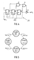
- FIG 4 shows a further embodiment of a frequency detector 14B .
- the detector comprises three D-type flip flops (Q4, Q5, Q6), an AND-gate (42), a NOR-gate (44) and a tristate driver (46).
- This frequency detector is provided with the inputs F ref2 and VCO2 and an output FO2. The functioning of this detector is illustrated by the state event diagram of Figure 5.
- the frequency detector 14B awaits a rising edge in the VCO signal on input VCO2, on which the flip flop Q6 is set to "one".
- the high output signal of flip flop Q6 resets both flip flops Q4 and Q5 and generates the pump-down signal at the output FO2 through the tristate driver (46), which has been enabled via NOR-gate 44.
- the flip flop Q6 On the next rising edge on the input VCO2, the flip flop Q6 takes the "zero" state over from flip flop Q5 and renders the tristate driver (46) inactive. At this instant the first state has been reached again and a new cycle of states may be started.
- the output FO2 generates a "pump-up” signal during a full period of the reference frequency and afterwards generates a “pump-down” signal during the following full period of the VCO output signal.
- a control voltage for the VCO 12 is generated. (See Figure 1).
Landscapes
- Engineering & Computer Science (AREA)
- Power Engineering (AREA)
- Stabilization Of Oscillater, Synchronisation, Frequency Synthesizers (AREA)
Claims (7)
- Circuit à verrouillage de phase (PLL) comprenant :- un oscillateur commandé en tension (VCO) (12) avec une sortie d'oscillateur qui est couplée à une première entrée d'un détecteur de fréquence (14) et à une première entrée d'un détecteur de phase (10), les sorties des détecteurs de fréquence et de phase étant couplées respectivement à une première et une seconde entrée d'un filtre de boucle (R1, R2, CF) dont la sortie est couplée à une entrée de commande du VCO (12);- le détecteur de phase (10) étant pourvu d'une entrée de données destinée à recevoir un signal de données (DATIN) et comprenant un circuit de comparaison numérique produisant un signal de sortie suite à une séquence de comparaisons d'un cycle du signal de données avec un cycle du signal du VCO, le circuit de comparaison étant déclenché chaque fois par le démarrage d'un signal de données (DATIN) et le signal de sortie produit se trouvant soit dans un premier état (PU) à partir du départ d'un signal de données jusqu'à la transition suivante du signal de sortie d'oscillateur (VCOIN) si le signal de sortie d'oscillateur est à un premier état au départ, soit dans un second état (PD) pendant l'intervalle de temps complet suivant, dans lequel le signal de sortie d'oscillateur se trouve dans le premier état, si le signal de sortie d'oscillateur se trouve dans un second état au départ;- le détecteur de fréquence (14) étant pourvu d'une entrée de référence destinée à recevoir une fréquence de référence (FREF);
étant entendu que la sortie (FO₁, FO₂) du détecteur de fréquence provient d'un premier niveau de tension qui est actif ou inactif et d'un second niveau de tension qui est actif ou inactif, le détecteur de fréquence (14) comprenant, en outre :- des moyens de repositionnement (Q₆, Q₈, Q₁₀) pour terminer un cycle de comparaison et faire démarrer un nouveau cycle,- des moyens de sélection (Q₇-Q₁₀, 32, 34, Q₄-Q₆, 42, 44) peur activer le premier niveau de tension pendant une première partie d'un cycle de comparaison et pour activer le second niveau de tension pendant une seconde partie d'un cycle de comparaison, la seconde partie étant non coïncidente avec la première partie;- la différence de longueurs de la première et de la seconde partie étant égale à zéro lorsque les signaux à la première entrée et à l'entrée de référence du détecteur de fréquence ont la même fréquence, et le signe de la différence correspondant au signe de la différence des fréquences entre les signaux à la première entrée et à l'entrée de référence. - Circuit PLL suivant la revendication 1, caractérisé en ce que le détecteur de fréquence (14A) comprend une première (Q₇), une deuxième (Q₈), une troisième (Q₉) et une quatrième (Q₁₀) bascule de type D (FF), l'entrée D de la première bascule (Q₇) et de la troisième bascule (Q₉) recevant une valeur binaire constante (+); les entrées d'horloge (CLK) de la première bascule (Q₇) et de la deuxième bascule (Q₈) étant connectées à l'entrée de référence (FREF), les entrées d'horloge (CLK) de la troisième bascule (Q₉) et de la quatrième bascule (Q₁₀) étant connectées à la première entrée du détecteur de fréquence (VCO); les sorties non inverseuses de la première bascule (Q₇) et de la troisième bascule (Q₉) étant connectées respectivement aux entrées de la deuxième bascule (Q₈) et de la quatrième bascule (Q₁₀) dont les sorties non inverseuses sont connectées aux entrées d'un circuit-porte NON ET constituant le moyen de repositionnement, dont la sortie est connectée à l'entrée de repositionnement (RST) des bascules (Q₇-Q₁₀) du détecteur de fréquence; le détecteur de fréquence (14A) comprenant, en outre, un premier et un deuxième circuit-porte NON OU à deux entrées, ainsi qu'un premier et un deuxième circuit-porte NON OU à trois entrées (32), les sorties des circuits-portes NON OU à trois entrées étant connectées à une entrée de commande respective d'un premier et d'un deuxième driver triétats (34), dont les sorties sont interconnectées pour former la sortie du détecteur de fréquence (FO₁); les sorties inverseuses de la première bascule (Q₇) et de la troisième bascule (Q₉) étant connectées à une entrée respective du premier et du deuxième circuit-porte NON OU à deux entrées (32); les sorties non inverseuses de la deuxième bascule (Q₈) et de la quatrième bascule (Q₁₀) étant connectées à la deuxième entrée respective du premier et du deuxième circuit-porte NON OU à deux entrées (32), ainsi qu'à une entrée respective du deuxième et du premier circuit-porte NON OU à trois entrées (32), ces derniers circuits-portes NON OU étant connectés par leur troisième entrée à la sortie respective du deuxième et du premier circuit-porte NON OU pour produire des signaux binaires complémentaires sur les sorties du premier et du second driver triétats (34).
- Circuit PLL suivant la revendication 1, caractérisé en ce que le détecteur de fréquence (14B) comprend une cinquième (Q₄), une sixième (Q₅) et une septième (Q₆) bascule de type D (FF), la première entrée (VCO₂) du détecteur de fréquence étant connectée à l'entrée d'horloge (CLK) de la septième bascule (Q₆); les entrées d'horloge (CLK) de la cinquième bascule (Q₄) et de la sixième bascule (Q₅) étant connectées à une entrée de référence (FREF2); des entrées de repositionnement (RST) de ces dernières bascules étant connectées à la sortie non inverseuse de la septième bascule (Q₆), à une entrée d'un troisième driver triétats (46) et à une première entrée d'un premier circuit-porte NON OU (44), dont la sortie est connectée à une entrée de commande du troisième driver triétats (46); les sorties non inverseuses de la cinquième bascule (Q₄) et de la sixième bascule (Q₅) étant connectées respectivement aux entrées D de la sixième bascule (Q₅) et de la septième bascule (Q₆); l'entrée (D) de la cinquième bascule (Q₄) recevant une valeur binaire constante; la sortie non inverseuse de la cinquième bascule (Q₄) étant, en outre, connectée à une première entrée d'un premier circuit-porte ET (42), dont la seconde entrée est connectée à la sortie inverseuse de la sixième bascule (Q₅) et dont la sortie est connectée à la seconde entrée du premier circuit-porte NON OU (44).
- Circuit PLL suivant la revendication 1, 2 ou 3 :- dans lequel la sortie du détecteur de phase présente un premier niveau de tension qui est actif ou inactif et un second niveau de tension qui est actif ou inactif, et dans lequel le premier niveau de tension est activé si le signal de sortie d'oscillateur (VCOIN) se trouve dans un premier état au départ du signal de données (DATIN) et est inactivé à la transition suivante du signal de données, caractérisé en ce que :- le détecteur de phase comprend :- un dispositif de sélection de période (21, 22, 23) pour activer le second niveau de tension (DD) pendant une demi-période du signal de sortie d'oscillateur (VCOIN) qui est le premier signal de demi-période après le démarrage d'un cycle,- le démarrage du cycle étant activé si le signal de sortie d'oscillateur (VCOIN) se trouve dans un second état au départ du signal de données (DATIN).
- Circuit PLL suivant la revendication 4, caractérisé en ce que le circuit de comparaison comprend une huitième (21), une neuvième (22) et une dixième (23) bascule de type D; la huitième (21) et la neuvième (22) bascule de type D étant connectées, par leur entrée d'horloge, à l'entrée de données (DATIN), la dixième bascule de type D (23) étant connectée par son entrée d'horloge, à l'entrée de repositionnement de la huitième bascule D (21) et à la première entrée (VCOIN).
- Circuit PLL suivant la revendication 4 ou 5, caractérisé en ce qu'au moins une sortie (PU, PD) du détecteur de phase (10) se trouve dans un état de haute impédance lorsque les deux niveaux de tension sont inactifs.
- Circuit PLL suivant la revendication 4, 5 ou 6, caractérisé en ce que le détecteur de phase comprend une huitième (21), une neuvième (22) et une dixième (23) bascule de type D (FF), chacune avec une entrée de données D, une sortie non inverseuse et une sortie inverseuse, une entrée d'horloge et une entrée de repositionnement; les entrées d'horloge de la huitième bascule (21) et de la neuvième bascule (22) étant couplées à l'entrée de données (DATIN) du détecteur de phase, l'entrée d'horloge de la dixième bascule (23) étant couplée à l'entrée de repositionnement de la huitième bascule (21); la première entrée (VCOIN) du détecteur de phase (10) étant connectée à l'entrée D de la neuvième bascule (22) et, par l'intermédiaire d'un premier inverseur (24), à l'entrée de repositionnement de la huitième bascule (21), la première entrée (VCOIN) étant, en outre, connectée à une première entrée d'un premier circuit-porte NON ET (25), dont la seconde entrée est connectée à la sortie inverseuse de la neuvième bascule (22) et dont la sortie est connectée à l'entrée de repositionnement de la dixième bascule (23), la sortie inverseuse de la dixième bascule (23) étant connectée à l'entrée de repositionnement de la neuvième bascule (22) et à une entrée de commande d'un premier driver triétats (28); la sortie non inverseuse de la neuvième bascule (22) étant connectée à l'entrée D de la dixième bascule (23); la sortie inverseuse de la huitième bascule (21) étant connectée à une entrée de commande d'un deuxième driver triétats (26) et l'entrée D de la huitième bascule (21) recevant une valeur binaire constante (+ 5V); les sorties des premier et deuxième drivers triétats (26, 28), qui produisent des signaux binaires complémentaires (PU, PD) lors de l'activation des entrées de commande, étant interconnectées pour former la sortie du détecteur de phase.
Applications Claiming Priority (4)
| Application Number | Priority Date | Filing Date | Title |
|---|---|---|---|
| US619093 | 1984-06-11 | ||
| US619096 | 1984-06-11 | ||
| US06/619,093 US4583053A (en) | 1984-06-11 | 1984-06-11 | Phase detector insensitive to missing pulses |
| US06/619,096 US4594564A (en) | 1984-06-11 | 1984-06-11 | Frequency detector for use with phase locked loop |
Publications (3)
| Publication Number | Publication Date |
|---|---|
| EP0164806A2 EP0164806A2 (fr) | 1985-12-18 |
| EP0164806A3 EP0164806A3 (en) | 1987-08-05 |
| EP0164806B1 true EP0164806B1 (fr) | 1992-03-18 |
Family
ID=27088413
Family Applications (1)
| Application Number | Title | Priority Date | Filing Date |
|---|---|---|---|
| EP19850200903 Expired EP0164806B1 (fr) | 1984-06-11 | 1985-06-07 | Circuit PLL |
Country Status (3)
| Country | Link |
|---|---|
| EP (1) | EP0164806B1 (fr) |
| CA (1) | CA1247202A (fr) |
| DE (1) | DE3585640D1 (fr) |
Families Citing this family (4)
| Publication number | Priority date | Publication date | Assignee | Title |
|---|---|---|---|---|
| JPH0787362B2 (ja) * | 1986-03-17 | 1995-09-20 | 日本電気株式会社 | 位相同期ル−プ |
| IT1223524B (it) * | 1987-12-18 | 1990-09-19 | Honeywell Bull Spa | Circuito ad aggancio di fase autotarante |
| DE3912838A1 (de) * | 1989-04-19 | 1990-10-25 | Thomson Brandt Gmbh | Pll-schaltung zum erzeugen eines taktsignals in einem recorder |
| CN1066392C (zh) * | 1996-01-18 | 2001-05-30 | 阮树成 | 一种快速精密锁相高频热合机伺服调谐装置 |
Family Cites Families (2)
| Publication number | Priority date | Publication date | Assignee | Title |
|---|---|---|---|---|
| GB1436933A (en) * | 1974-09-26 | 1976-05-26 | Mullard Ltd | Phase and/or frequency comparators |
| DE3115057C2 (de) * | 1981-04-14 | 1984-03-29 | Siemens AG, 1000 Berlin und 8000 München | Phasenregelkreis mit einem digitalen Phasendiskriminator |
-
1985
- 1985-06-06 CA CA000483307A patent/CA1247202A/fr not_active Expired
- 1985-06-07 EP EP19850200903 patent/EP0164806B1/fr not_active Expired
- 1985-06-07 DE DE8585200903T patent/DE3585640D1/de not_active Expired - Lifetime
Also Published As
| Publication number | Publication date |
|---|---|
| DE3585640D1 (de) | 1992-04-23 |
| EP0164806A2 (fr) | 1985-12-18 |
| CA1247202A (fr) | 1988-12-20 |
| EP0164806A3 (en) | 1987-08-05 |
Similar Documents
| Publication | Publication Date | Title |
|---|---|---|
| US5015970A (en) | Clock recovery phase lock loop having digitally range limited operating window | |
| EP0866559B1 (fr) | Boucle à verrouillage de phase | |
| US7209009B2 (en) | Controlling a voltage controlled oscillator in a bang-bang phase locked loop | |
| US3983498A (en) | Digital phase lock loop | |
| US5870002A (en) | Phase-frequency lock detector | |
| EP0449659B1 (fr) | Détecteur de phase à trois états à caractéristique linéarisée | |
| US7236028B1 (en) | Adaptive frequency variable delay-locked loop | |
| US5142246A (en) | Multi-loop controlled VCO | |
| US5834950A (en) | Phase detector which eliminates frequency ripple | |
| US5734301A (en) | Dual phase-locked loop clock synthesizer | |
| US5579352A (en) | Simplified window de-skewing in a serial data receiver | |
| GB2091961A (en) | Phase tolerant bit synchronizer for digital signals | |
| US6005425A (en) | PLL using pulse width detection for frequency and phase error correction | |
| US5307028A (en) | Phase-and-frequency mode/phase mode detector with the same gain in both modes | |
| EP0195500B1 (fr) | Circuit charge-décharge pour boucle d'asservissement de phase | |
| US5592515A (en) | Fully digital data separator and frequency multiplier | |
| US5457428A (en) | Method and apparatus for the reduction of time interval error in a phase locked loop circuit | |
| US6157218A (en) | Phase-frequency detection with no dead zone | |
| EP0287776B1 (fr) | Détecteur de données à verrouillage de phase | |
| US6853223B2 (en) | Phase comparator and clock recovery circuit | |
| US6249188B1 (en) | Error-suppressing phase comparator | |
| US7183861B2 (en) | Circuits and methods for detecting phase lock | |
| EP0164806B1 (fr) | Circuit PLL | |
| US20050057290A1 (en) | Coarse frequency detector system and method thereof | |
| JP2917892B2 (ja) | 半導体集積回路 |
Legal Events
| Date | Code | Title | Description |
|---|---|---|---|
| PUAI | Public reference made under article 153(3) epc to a published international application that has entered the european phase |
Free format text: ORIGINAL CODE: 0009012 |
|
| AK | Designated contracting states |
Designated state(s): DE FR GB IT |
|
| PUAL | Search report despatched |
Free format text: ORIGINAL CODE: 0009013 |
|
| AK | Designated contracting states |
Kind code of ref document: A3 Designated state(s): DE FR GB IT |
|
| 17P | Request for examination filed |
Effective date: 19880204 |
|
| 17Q | First examination report despatched |
Effective date: 19900119 |
|
| GRAA | (expected) grant |
Free format text: ORIGINAL CODE: 0009210 |
|
| AK | Designated contracting states |
Kind code of ref document: B1 Designated state(s): DE FR GB IT |
|
| PG25 | Lapsed in a contracting state [announced via postgrant information from national office to epo] |
Ref country code: IT Free format text: LAPSE BECAUSE OF FAILURE TO SUBMIT A TRANSLATION OF THE DESCRIPTION OR TO PAY THE FEE WITHIN THE PRESCRIBED TIME-LIMIT;WARNING: LAPSES OF ITALIAN PATENTS WITH EFFECTIVE DATE BEFORE 2007 MAY HAVE OCCURRED AT ANY TIME BEFORE 2007. THE CORRECT EFFECTIVE DATE MAY BE DIFFERENT FROM THE ONE RECORDED. Effective date: 19920318 |
|
| REF | Corresponds to: |
Ref document number: 3585640 Country of ref document: DE Date of ref document: 19920423 |
|
| ET | Fr: translation filed | ||
| PLBE | No opposition filed within time limit |
Free format text: ORIGINAL CODE: 0009261 |
|
| STAA | Information on the status of an ep patent application or granted ep patent |
Free format text: STATUS: NO OPPOSITION FILED WITHIN TIME LIMIT |
|
| 26N | No opposition filed | ||
| REG | Reference to a national code |
Ref country code: FR Ref legal event code: CD |
|
| PGFP | Annual fee paid to national office [announced via postgrant information from national office to epo] |
Ref country code: GB Payment date: 19960603 Year of fee payment: 12 |
|
| PGFP | Annual fee paid to national office [announced via postgrant information from national office to epo] |
Ref country code: FR Payment date: 19960626 Year of fee payment: 12 |
|
| PGFP | Annual fee paid to national office [announced via postgrant information from national office to epo] |
Ref country code: DE Payment date: 19960823 Year of fee payment: 12 |
|
| PG25 | Lapsed in a contracting state [announced via postgrant information from national office to epo] |
Ref country code: GB Free format text: LAPSE BECAUSE OF NON-PAYMENT OF DUE FEES Effective date: 19970607 |
|
| GBPC | Gb: european patent ceased through non-payment of renewal fee |
Effective date: 19970607 |
|
| PG25 | Lapsed in a contracting state [announced via postgrant information from national office to epo] |
Ref country code: FR Free format text: LAPSE BECAUSE OF NON-PAYMENT OF DUE FEES Effective date: 19980227 |
|
| PG25 | Lapsed in a contracting state [announced via postgrant information from national office to epo] |
Ref country code: DE Free format text: LAPSE BECAUSE OF NON-PAYMENT OF DUE FEES Effective date: 19980303 |
|
| REG | Reference to a national code |
Ref country code: FR Ref legal event code: ST |
|
| REG | Reference to a national code |
Ref country code: FR Ref legal event code: ST |