EP0164934A2 - Raumtemperatur-Metalldampflaser - Google Patents
Raumtemperatur-Metalldampflaser Download PDFInfo
- Publication number
- EP0164934A2 EP0164934A2 EP85303506A EP85303506A EP0164934A2 EP 0164934 A2 EP0164934 A2 EP 0164934A2 EP 85303506 A EP85303506 A EP 85303506A EP 85303506 A EP85303506 A EP 85303506A EP 0164934 A2 EP0164934 A2 EP 0164934A2
- Authority
- EP
- European Patent Office
- Prior art keywords
- metal
- cathode
- sputtering
- optical cavity
- metal vapour
- Prior art date
- Legal status (The legal status is an assumption and is not a legal conclusion. Google has not performed a legal analysis and makes no representation as to the accuracy of the status listed.)
- Withdrawn
Links
- 229910052751 metal Inorganic materials 0.000 title claims abstract description 123
- 239000002184 metal Substances 0.000 title claims abstract description 123
- 238000004544 sputter deposition Methods 0.000 claims abstract description 72
- 230000003287 optical effect Effects 0.000 claims abstract description 39
- 239000012212 insulator Substances 0.000 claims description 11
- 238000000034 method Methods 0.000 claims description 7
- 239000007789 gas Substances 0.000 abstract description 20
- 239000011261 inert gas Substances 0.000 abstract 2
- XKRFYHLGVUSROY-UHFFFAOYSA-N Argon Chemical compound [Ar] XKRFYHLGVUSROY-UHFFFAOYSA-N 0.000 description 14
- 230000005284 excitation Effects 0.000 description 12
- 150000002739 metals Chemical class 0.000 description 9
- 229910052756 noble gas Inorganic materials 0.000 description 8
- 229910052786 argon Inorganic materials 0.000 description 7
- 239000006091 Macor Substances 0.000 description 6
- 229910021645 metal ion Inorganic materials 0.000 description 6
- 230000007704 transition Effects 0.000 description 6
- 230000007935 neutral effect Effects 0.000 description 5
- 239000000919 ceramic Substances 0.000 description 4
- 150000002500 ions Chemical group 0.000 description 4
- 238000010494 dissociation reaction Methods 0.000 description 3
- 230000005593 dissociations Effects 0.000 description 3
- 230000008569 process Effects 0.000 description 3
- RYGMFSIKBFXOCR-UHFFFAOYSA-N Copper Chemical compound [Cu] RYGMFSIKBFXOCR-UHFFFAOYSA-N 0.000 description 2
- 150000001875 compounds Chemical class 0.000 description 2
- 238000007796 conventional method Methods 0.000 description 2
- 229910052802 copper Inorganic materials 0.000 description 2
- 239000010949 copper Substances 0.000 description 2
- 239000011521 glass Substances 0.000 description 2
- 238000004519 manufacturing process Methods 0.000 description 2
- 239000000203 mixture Substances 0.000 description 2
- 238000006276 transfer reaction Methods 0.000 description 2
- 230000008016 vaporization Effects 0.000 description 2
- 241000009298 Trigla lyra Species 0.000 description 1
- 230000009471 action Effects 0.000 description 1
- 239000000956 alloy Substances 0.000 description 1
- 229910045601 alloy Inorganic materials 0.000 description 1
- 239000004411 aluminium Substances 0.000 description 1
- 229910052782 aluminium Inorganic materials 0.000 description 1
- XAGFODPZIPBFFR-UHFFFAOYSA-N aluminium Chemical compound [Al] XAGFODPZIPBFFR-UHFFFAOYSA-N 0.000 description 1
- 239000004020 conductor Substances 0.000 description 1
- 238000010276 construction Methods 0.000 description 1
- 238000013461 design Methods 0.000 description 1
- 230000005281 excited state Effects 0.000 description 1
- PCHJSUWPFVWCPO-UHFFFAOYSA-N gold Chemical compound [Au] PCHJSUWPFVWCPO-UHFFFAOYSA-N 0.000 description 1
- 229910052737 gold Inorganic materials 0.000 description 1
- 239000010931 gold Substances 0.000 description 1
- 230000005283 ground state Effects 0.000 description 1
- 238000010438 heat treatment Methods 0.000 description 1
- 239000000463 material Substances 0.000 description 1
- 150000002736 metal compounds Chemical class 0.000 description 1
- 229910001507 metal halide Inorganic materials 0.000 description 1
- 150000005309 metal halides Chemical class 0.000 description 1
- 238000012986 modification Methods 0.000 description 1
- 230000004048 modification Effects 0.000 description 1
- 229910052754 neon Inorganic materials 0.000 description 1
- GKAOGPIIYCISHV-UHFFFAOYSA-N neon atom Chemical compound [Ne] GKAOGPIIYCISHV-UHFFFAOYSA-N 0.000 description 1
- 150000002835 noble gases Chemical class 0.000 description 1
- 238000005457 optimization Methods 0.000 description 1
- 239000010453 quartz Substances 0.000 description 1
- 230000000717 retained effect Effects 0.000 description 1
- VYPSYNLAJGMNEJ-UHFFFAOYSA-N silicon dioxide Inorganic materials O=[Si]=O VYPSYNLAJGMNEJ-UHFFFAOYSA-N 0.000 description 1
- 125000006850 spacer group Chemical group 0.000 description 1
- 230000003068 static effect Effects 0.000 description 1
- 238000012546 transfer Methods 0.000 description 1
- 238000009834 vaporization Methods 0.000 description 1
- 239000003039 volatile agent Substances 0.000 description 1
Images

Classifications
-
- H—ELECTRICITY
- H01—ELECTRIC ELEMENTS
- H01J—ELECTRIC DISCHARGE TUBES OR DISCHARGE LAMPS
- H01J37/00—Discharge tubes with provision for introducing objects or material to be exposed to the discharge, e.g. for the purpose of examination or processing thereof
- H01J37/32—Gas-filled discharge tubes
- H01J37/32431—Constructional details of the reactor
- H01J37/3244—Gas supply means
-
- H—ELECTRICITY
- H01—ELECTRIC ELEMENTS
- H01J—ELECTRIC DISCHARGE TUBES OR DISCHARGE LAMPS
- H01J37/00—Discharge tubes with provision for introducing objects or material to be exposed to the discharge, e.g. for the purpose of examination or processing thereof
- H01J37/32—Gas-filled discharge tubes
- H01J37/34—Gas-filled discharge tubes operating with cathodic sputtering
-
- H—ELECTRICITY
- H01—ELECTRIC ELEMENTS
- H01S—DEVICES USING THE PROCESS OF LIGHT AMPLIFICATION BY STIMULATED EMISSION OF RADIATION [LASER] TO AMPLIFY OR GENERATE LIGHT; DEVICES USING STIMULATED EMISSION OF ELECTROMAGNETIC RADIATION IN WAVE RANGES OTHER THAN OPTICAL
- H01S3/00—Lasers, i.e. devices using stimulated emission of electromagnetic radiation in the infrared, visible or ultraviolet wave range
- H01S3/02—Constructional details
- H01S3/03—Constructional details of gas laser discharge tubes
- H01S3/031—Metal vapour lasers, e.g. metal vapour generation
Definitions
- This invention relates to metal vapour lasers.
- a major cause of technical difficulties and limitations in the operation of metal vapour lasers is the method by which the metal atoms are established within the laser discharge volume.
- Conventional methods of vaporizing the metal to provide metal atoms have limitations.
- Direct vaporization of the metal using either an external oven or discharge heating requires high temperatures, about 1500°C for copper, to be achieved.
- High power copper and gold lasers exploit the discharge energy to heat a tube.
- the need for ovens also makes it difficult to construct the fast discharge circuitry needed for excitation of other potentially interesting self-terminating neutral metal laser transitions.
- continuous-wave (cw) metal ion lasers use a dc discharge which produces both dissociation and excitation.
- the dissociation is virtually complete so that the vapour pressure is controlled by tube temperature and consequently the excitation may be separately optimized (Brandt and Piper 1977).
- Another commonly used method of metal production is by sputtering the metal atoms from a cathode of the desired material (Gersternberger et al 1980).
- the-metal density required to support laser action has been produced by cathodic sputtering using a hollow cathode discharge.
- Use of a hollow cathode also greatly increases the extent of ionization in the buffer gas over that found in the more common positive column type gas discharge.
- the invention may be said to reside in a metal vapour laser including an optical cavity, sputtering means for sputtering a metal to provide a metal vapour beam in the cavity, said sputtering means comprising a sputtering cathode and anode for producing an electrical discharge to sputter said metal and means for producing a gas stream for entraining the sputtered metal into a metal vapour beam within said optical cavity.
- the sputtering means sputters the metal by means of-an electrical discharge the device can be operated at room temperature.
- the invention in a second aspect may be said to reside in a metal vapour laser having an optical cavity, sputtering means for sputtering a metal to produce a metal vapour, said sputtering means including first electrical discharge means for sputtering the metal and said laser having second separate electrical discharge means arranged in said optical cavity for exciting the metal vapour.
- this aspect of the invention provides separate electrical discharge means for sputtering the metal and for exciting the metal vapour optimum metal vapour concentration can be obtained for any particular metal as well as optimum concentration of the electrical discharge for exciting the metal vapour.
- the sputtering means further includes means for producing a gaseous jet for entraining sputtered metal and forming a metal vapour beam in the optical cavity.
- the sputtering means is located at one end of the optical cavity and the other end of the optical cavity is provided with an outlet aperture which communicates with a chamber, the chamber having an outlet for connection to a vacuum pump for drawing the metal vapour beam entrained in the gas stream coaxially through the optical cavity.
- the sputtering means comprises a cathode, a cylindrical insulator surrounding said cathode, the insulator having an opening for exposing the cathode to the optical cavity, an anode disposed adjacent to the portion of the cathode which is exposed to the optical cavity, said anode being spaced from the cathode and an annular channel between said anode and the portion of the cathode exposed to the cavity for supplying a gaseous jet such that when electrical discharge occurs between the anode and the portion of the cathode exposed to the optical cavity the metal of the cathode is sputtered and entrained in the gas flow to produce a metal vapour beam in the optical cavity.
- the cathode may comprise a sputtering cathode formed from the metal from which the metal vapour is produced or the cathode may comprise a cathode plug having a sputtering cathode portion located at its end which is exposed to the optical cavity.
- a gap is provided between the insulator and the portion of the cathode which is to be sputtered.
- the invention in a third aspect may also be said to reside in a method of exciting a metal vapour beam comprising the steps of producing the metal vapour beam, arranging an electrode adjacent to said beam and causing electrical discharge from said electrode to said beam.
- the electrode comprises a ringshaped electrode through which the beam passes.
- the electrode may be in the form of a pin arranged perpendicular to the beam.
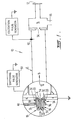
- a metal vapour laser 10 which comprises an optical cavity 12 formed of non-conducting material such as glass which has a sputtering means 14 at one end and a chamber 16 having a quartz window 17 at the other end.
- the sputtering means 14 comprises an annular T-shaped sputtering cathode 18 which has an optical outlet cavity 20 axially therethrough with a means for excluding the sputtering discharge from the cavity.
- a stem portion 22 of the cathode 18 is retained in a discharge arrester 24.
- the arrester 24 is cylindrical in nature and is open at both ends so that a portion of the stem 22 is exposed to the cavity 12 and so that the cathode 18 can be removed from the arrester 24.
- the arrester is comprised of three parts: an inner cylinder of Macor (trade mark) ceramic 26 an outer cylinder and cap of Macor ceramic 28 spaced from the inner cylinder 26 to provide an annular passage 33 for the passage of noble gas across the end of the cathode stem 22.
- the inner Macor cylinder 26 and outer Macor cylinder 28 are fixed in position by the locking ring 36 which defines an annular chamber 38 which communicates with the passage 33 and noble gas inlet 40.
- the cathode 18 is sealed in the arrester 24 by an 0-ring 30.
- the arrester is sealed to an annular anode 32 by an O-ring 31 immediately behind an opening 34 in the anode 32 to expose the cathode 18 to the cavity 12.
- the anode 32 which is grounded forms one end wall of the cavity 12.
- end of the stem portion 22 of the cathode 18 which is to be sputtered is of reduced diameter and spaced from the arrestor 24.
- the chamber 16 at the other end of the cavity 12 has an outlet 44 for connection to a vacuum pump (not shown).
- a sputtering pulse generator 50 is provided for applying pulsing current to the cathode 18.
- the electrical discharge sputters the metal at the reduced diameter end portion of the cathode stem 22 and the sputtered metal is entrained in a jet stream produced when argon gas enters inlet 40, passes through annular chamber 38 and the passage 33 and which is then drawn in the direction of arrow B through opening 54, which joins the cavity 12 with the chamber 16, by the vacuum pump coupled to outlet 44.
- the cavity 12 contains a noble gas atmosphere which for economic reasons is preferably argon but may be neon or any mixture of noble gases.
- An electrode 55 (not shown in detail) is arranged adjacent the opening 54 and is coupled to an excitation pulse generator for providing an electrical discharge to excite the metal vapour beam.
- the electrode can be a pin type electrode arranged adjacent to the beam or can comprise a ring type electrode through which the beam passes. It has been found that the electronic discharge is drawn directly into the metal vapour beam rather than into the noble gas atmosphere surrounding the beam and therefore minimal current is required to provide the electrical discharge for exciting the metal vapour beam.
- a glass disc insulator 35 is provided to shield the end wall 37 from the electrode 55. The insulator 35 has an annular opening which coincides with the opening 34.
- FIG. 2 shows a second embodiment of the sputtering means which comprises a cathode plug 60 held by an O-ring 62 in a Macor ceramic cylinder 64.
- the end of stem portion 66 of the plug 60 is in contact with a sputtering cathode 68 formed from the metal from which the metal vapour is to be produced.
- a second annular Macor ceramic insulator 70 is disposed around the inner end of the insulator 64 and is spaced therefrom by spacer ribs and feet 72.
- the space between the insulator 64 and 70 forms a gas flow passage which terminates in an annular outlet adjacent the sputtering cathode 68.
- the gas flow passage communicates with an annular chamber 74 which has a gas inlet 76.
- a grounded anode plate 80 is arranged at the inner end of the insulator 70 and includes an opening 82 for exposing the sputtering cathode 68 to the optical cavity (not shown in Figure 2).
- the metal of the sputtering cathode is sputtered and entrained in an argon gas jet stream which is produced by connecting an argon gas source to the gas inlet 68. This enables argon gas to flow through the annular chamber 74, the gas flow passage and the optical cavity with the assistance of the vacuum pump described with reference to Figure 1.
- the sputtered metal is entrained in the argon jet stream to produce a metal vapour beam in the cavity.
- the power supply for producing the discharge current between the anode 80 and the cathode 68 generally includes a pulse voltage source and a dc simmer voltage source.
- the sputtering means described with reference to Figures 1 and 2 entrains the metal atoms in a gas jet, to form a collimated metal vapour beam with a local concentration of the order of 10 cm .
- the gas flow in this device, decouples the processes responsible for the sputtering and subsequent excitation of the metal atoms, allowing separate discharges and independent control of the metal atom density and excitation discharge current.
- the highest concentration achieved, at a current density of 550 mA cm 2 is similar to that obtained at the same current density in hollow cathode metal ion sputtering lasers.
- the geometry of the hollow cathode discharge requires a much larger cathode area to achieve a sufficient gain path, and necessitates a cathode current one to two orders of magnitude higher than is used in the preferred embodiment of the present invention.
- the sputtering means could comprise a sputtering cathode, arrester and anode of geometry other than circular or annular to produce a planar sheet of metal vapour, together with a cylindrical hollow cathode with a slit extending along its length for receiving said planar beam of metal vapour so that the metal atoms are excited by means of a discharge within said hollow cathode.
- the preferred embodiment of the present invention provides the following advantages:-Separate electrical discharges for producing metal vapour and for exciting the metal vapour which provides great flexibility in the control of the concentration of the excitation discharge.
- Sputtering of the cathode enables a wide range of metals or alloys or even compounds to be used as an excitation medium in the laser and also enables simultaneous operation using several different metals. Furthermore the vapour pressure of each of the different metals can be separately controlled.
- the present device is also simple in structure and inexpensive to produce.
- the threshold discharge current for a continuous-wave laser would be significantly reduced due to more efficient sputtering and due to the independent optimization of the sputtering and excitation processes.
- Simultaneous operation on several wavelengths could be achieved by means of separate, independently optimized sputtering of the appropriate metals. This would allow independent control of the partial pressure of each metal in the vapour.
- a wide range of metals can be sputtered.
- the gas-jet assisted sputtering enables "difficult" metals such as aluminium to be efficiently sputtered.
- this laser could be applied to most metals and should permit the operation of new transitions.
Landscapes
- Physics & Mathematics (AREA)
- Engineering & Computer Science (AREA)
- Plasma & Fusion (AREA)
- Electromagnetism (AREA)
- Chemical & Material Sciences (AREA)
- Analytical Chemistry (AREA)
- Optics & Photonics (AREA)
- Lasers (AREA)
- Physical Vapour Deposition (AREA)
Applications Claiming Priority (3)
| Application Number | Priority Date | Filing Date | Title |
|---|---|---|---|
| AU5528/84 | 1984-06-15 | ||
| AUPG552884 | 1984-06-15 | ||
| AU42296/85A AU575161B2 (en) | 1984-06-15 | 1985-05-10 | Room temperature metal vapour laser |
Publications (2)
| Publication Number | Publication Date |
|---|---|
| EP0164934A2 true EP0164934A2 (de) | 1985-12-18 |
| EP0164934A3 EP0164934A3 (de) | 1987-11-04 |
Family
ID=25625924
Family Applications (1)
| Application Number | Title | Priority Date | Filing Date |
|---|---|---|---|
| EP85303506A Withdrawn EP0164934A3 (de) | 1984-06-15 | 1985-05-20 | Raumtemperatur-Metalldampflaser |
Country Status (1)
| Country | Link |
|---|---|
| EP (1) | EP0164934A3 (de) |
Cited By (1)
| Publication number | Priority date | Publication date | Assignee | Title |
|---|---|---|---|---|
| EP0230990A3 (de) * | 1986-01-24 | 1989-05-31 | Monash University | Raumtemperatur-Metalldampflaser |
Family Cites Families (1)
| Publication number | Priority date | Publication date | Assignee | Title |
|---|---|---|---|---|
| US3621460A (en) * | 1970-07-06 | 1971-11-16 | Us Army | Sputtered vapor laser |
-
1985
- 1985-05-20 EP EP85303506A patent/EP0164934A3/de not_active Withdrawn
Cited By (1)
| Publication number | Priority date | Publication date | Assignee | Title |
|---|---|---|---|---|
| EP0230990A3 (de) * | 1986-01-24 | 1989-05-31 | Monash University | Raumtemperatur-Metalldampflaser |
Also Published As
| Publication number | Publication date |
|---|---|
| EP0164934A3 (de) | 1987-11-04 |
Similar Documents
| Publication | Publication Date | Title |
|---|---|---|
| US4641313A (en) | Room temperature metal vapour laser | |
| US4713585A (en) | Ion source | |
| US4780608A (en) | Laser sustained discharge nozzle apparatus for the production of an intense beam of high kinetic energy atomic species | |
| US4730334A (en) | Ultraviolet metal ion laser | |
| US4980610A (en) | Plasma generators | |
| EP0965253A1 (de) | Verfahren und vorrichtung zum erzeugen eines plasmas | |
| US4641316A (en) | D.C. electron beam method and apparatus for continuous laser excitation | |
| JPH06220631A (ja) | マイクロ波強化スパッタリング装置 | |
| EP0164934A2 (de) | Raumtemperatur-Metalldampflaser | |
| US4545878A (en) | Method and apparatus for separating isotopes using electrophoresis in a discharge | |
| US4782267A (en) | In-situ wide area vacuum ultraviolet lamp | |
| US4788686A (en) | Gas-laser arrangement | |
| US4952294A (en) | Apparatus and method for in-situ generation of dangerous polyatomic gases, including polyatomic radicals | |
| US5898723A (en) | Metal vapor laser device | |
| JPH08102278A (ja) | イオンビーム発生装置及び方法 | |
| US4771435A (en) | Room temperature metal vapor laser | |
| US4540868A (en) | Plasma gun that reduces cathode contamination | |
| US4680770A (en) | Dual beam gas ion laser | |
| US4563258A (en) | Method and apparatus for separating isotopes using electrophoresis in a discharge | |
| CA1093628A (en) | Device and method of starting a long radiation source | |
| US5892788A (en) | Gas laser with dual plasma mixing | |
| Marcus et al. | The hollow cathode plume: A plasma emission source for solids | |
| Walther et al. | Production of atomic or molecular nitrogen ion beams using a multicusp and a microwave ion source | |
| JPH0831417B2 (ja) | プラズマ加工堆積装置 | |
| US4263533A (en) | Magnetically contained arc discharge lamp with crossed electric and magnetic fields |
Legal Events
| Date | Code | Title | Description |
|---|---|---|---|
| PUAI | Public reference made under article 153(3) epc to a published international application that has entered the european phase |
Free format text: ORIGINAL CODE: 0009012 |
|
| AK | Designated contracting states |
Designated state(s): AT BE CH DE FR GB IT LI LU NL SE |
|
| PUAL | Search report despatched |
Free format text: ORIGINAL CODE: 0009013 |
|
| AK | Designated contracting states |
Kind code of ref document: A3 Designated state(s): AT BE CH DE FR GB IT LI LU NL SE |
|
| 17P | Request for examination filed |
Effective date: 19880402 |
|
| 17Q | First examination report despatched |
Effective date: 19900322 |
|
| STAA | Information on the status of an ep patent application or granted ep patent |
Free format text: STATUS: THE APPLICATION IS DEEMED TO BE WITHDRAWN |
|
| 18D | Application deemed to be withdrawn |
Effective date: 19910907 |
|
| RIN1 | Information on inventor provided before grant (corrected) |
Inventor name: TOBIN, RODERICK C. Inventor name: PERRY, NIGEL D. |