EP0165055A2 - Photoresistbelichtungsverfahren und Gerät unter Verwendung eines Elektronenstrahls, dessen Energie und Ladung gesteuert werden - Google Patents
Photoresistbelichtungsverfahren und Gerät unter Verwendung eines Elektronenstrahls, dessen Energie und Ladung gesteuert werden Download PDFInfo
- Publication number
- EP0165055A2 EP0165055A2 EP85304167A EP85304167A EP0165055A2 EP 0165055 A2 EP0165055 A2 EP 0165055A2 EP 85304167 A EP85304167 A EP 85304167A EP 85304167 A EP85304167 A EP 85304167A EP 0165055 A2 EP0165055 A2 EP 0165055A2
- Authority
- EP
- European Patent Office
- Prior art keywords
- electron beam
- photoresist
- controlling
- projected
- incident
- Prior art date
- Legal status (The legal status is an assumption and is not a legal conclusion. Google has not performed a legal analysis and makes no representation as to the accuracy of the status listed.)
- Granted
Links
Images

Classifications
-
- B—PERFORMING OPERATIONS; TRANSPORTING
- B82—NANOTECHNOLOGY
- B82Y—SPECIFIC USES OR APPLICATIONS OF NANOSTRUCTURES; MEASUREMENT OR ANALYSIS OF NANOSTRUCTURES; MANUFACTURE OR TREATMENT OF NANOSTRUCTURES
- B82Y10/00—Nanotechnology for information processing, storage or transmission, e.g. quantum computing or single electron logic
-
- B—PERFORMING OPERATIONS; TRANSPORTING
- B82—NANOTECHNOLOGY
- B82Y—SPECIFIC USES OR APPLICATIONS OF NANOSTRUCTURES; MEASUREMENT OR ANALYSIS OF NANOSTRUCTURES; MANUFACTURE OR TREATMENT OF NANOSTRUCTURES
- B82Y40/00—Manufacture or treatment of nanostructures
-
- H—ELECTRICITY
- H01—ELECTRIC ELEMENTS
- H01J—ELECTRIC DISCHARGE TUBES OR DISCHARGE LAMPS
- H01J37/00—Discharge tubes with provision for introducing objects or material to be exposed to the discharge, e.g. for the purpose of examination or processing thereof
- H01J37/30—Electron-beam or ion-beam tubes for localised treatment of objects
- H01J37/317—Electron-beam or ion-beam tubes for localised treatment of objects for changing properties of the objects or for applying thin layers thereon, e.g. for ion implantation
- H01J37/3174—Particle-beam lithography, e.g. electron beam lithography
-
- H—ELECTRICITY
- H01—ELECTRIC ELEMENTS
- H01J—ELECTRIC DISCHARGE TUBES OR DISCHARGE LAMPS
- H01J2237/00—Discharge tubes exposing object to beam, e.g. for analysis treatment, etching, imaging
- H01J2237/30—Electron or ion beam tubes for processing objects
- H01J2237/317—Processing objects on a microscale
- H01J2237/3175—Lithography
- H01J2237/31793—Problems associated with lithography
- H01J2237/31796—Problems associated with lithography affecting resists
-
- Y—GENERAL TAGGING OF NEW TECHNOLOGICAL DEVELOPMENTS; GENERAL TAGGING OF CROSS-SECTIONAL TECHNOLOGIES SPANNING OVER SEVERAL SECTIONS OF THE IPC; TECHNICAL SUBJECTS COVERED BY FORMER USPC CROSS-REFERENCE ART COLLECTIONS [XRACs] AND DIGESTS
- Y10—TECHNICAL SUBJECTS COVERED BY FORMER USPC
- Y10S—TECHNICAL SUBJECTS COVERED BY FORMER USPC CROSS-REFERENCE ART COLLECTIONS [XRACs] AND DIGESTS
- Y10S430/00—Radiation imagery chemistry: process, composition, or product thereof
- Y10S430/143—Electron beam
Definitions
- This invention relates to the fabrication of semiconductor devices using electron beam aided processes, such as the use of an electron bean to trace an exposure pattern in the_photoresist or other film coated onto an underlying semiconductor or composite substrate. More specifically, the invention relates to a method of exposing the photoresist coating with an electron-beam where the accelerating voltage and the amount of charge lf the projected electron beam are controlled and correlated to thickness variations in the photoresist, as may result from variations in the underlying topography.
- the energy of the electron beam incident upon the photoresist and underlying structures or layers is controlled as the beam is deflected. This permits thorough exposure of the photoresist by the electron beam while minimizing ionizing radiation damage to the underlying semiconductor material, structures, insulating layers, and the like.
- FIGS 1A-1F illustrate a typical series of steps used in electron beam, photo aided, or lithographic processes to manufacture semiconductor devices.
- a semiconductor substrate 1 such as a slice or wafer of silicon or other composite has grown thereon an insulating oxide layer 2, such as silicon dioxide.
- a series of steps is undertaken to cut a window or pattern in the silicon dioxide layer and expose a predetermined area of the underlying substrate 1.
- a film of photoresist 3 is coated onto the entire surface of the oxide layer 2.
- the photoresist is sensitive to incident radiation, such as an electron beam, visible light, ultraviolet light, or X-rays.
- a traveling electron beam 4 is moved across the photoresist to expose selected portions.
- the beam is directed in a manner to expose the photoresist according to a pattern traced or "written" by the beam.
- This is referred to as maskless or direct processing, and it delineates an exposure pattern by writing directly on the photoresist.
- the electron beam has a shorter wavelength and greater depth of field than many other types of radiation, it is capable of forming very fine exposure patterns, and it eliminates the need to create a cumbersome physical mask, as used with ultraviolet processing, which is time consuming and very costly.
- the exposed portion is indicated by the stippled area 3a. That portion of the photoresist labeled 3b is not exposed to the incident radiation and is not affected thereby.
- the photoresist is subjected to a process that dissolves and removes the exposed photoresist 3a but does not affect the unexposed photoresist. This leaves a pair of spaced parallel strips 3b of unexposed photoresist separated by a channel 2a of the underlying oxide layer 2.
- the unexposed photoresist 3b and the oxide layer 2a are treated so as to remove the unprotected oxide, but not the unexposed photoresist 3b, in order to expose a channel la of the underlying material 1.
- the unexposed photoresist 3b has been stripped from the oxide layer in preparation for succeeding process steps, leaving a channel of bare silicon defined by strips of superposed silicon dioxide 2.
- circuit elements typically are on the order of a few microns in size or smaller, and they may be composed of layers on the order of only 0.01 microns deep.
- succeeding processing steps do not disturb the effects of earlier steps, and, for this reason, it is desirable to control the energy of the electron beam or other radiation used to expose the photoresist.
- the energy of the incident electron beam was not controlled to match the amount of energy required to expose the photoresist or the thickness or depth of the photoresist at a given location. Instead, the electron beam voltage and charge was fixed at a level high enough to expose the thickest portions of the photoresist layer without regard to any problems that might arise where the photoresist was thinner, or where there were other variations in the photoresist coating, or where the underlying structures were "tall," or where the underlying layers were susceptible to damage from the incident electron beam radiation.
- the electron beam had excess energy in some sectors and the electrons penetrated to the underlying layers or substrate, resulting in unwanted damage.
- unwanted damage was inflicted upon insulated gate field effect transistors (IGFET) when the accelerating voltage of the electron beam used to expose,the photoresist was too high and the electrons penetrated through the photoresist and overlying films to the gate insulator.
- IGFET insulated gate field effect transistors
- the electrons are accelerated to 20 to 25 kilovolts (KeV), or even as high as 50 KeV, and the photoresist is subjected to dosages of 20 to 30 microcoulombs per square centimeter.
- KeV kilovolts
- the incident electrons pass through typical thicknesses of photoresist, i.e. two to three microns, and damage the underlying films and semiconductor materials. This produces fixed positive charge and neutral traps, which are undesirable.
- a metalizing layer it was believed that such damage could be annealed by heating the semiconductor wafers in a hydrogen-containing ambient atmosphere in the 550-700° C range.
- the present invention is based upon the recognition that proper exposure of the photoresist is a function of the energy absorbed by it rather than the accelerating voltage of the electron beam or the amount of change carried by the beam alone. Stated otherwise, the extent of radiation damage is a function of the tootal energy absorbed in a given mass of material and root the energy per photon or energy per electron. Thuis, the present invention involves matching the eenergy of the incident electron beam and electron dose to the amount of energy locally required to thoroughly expose the photoresist. This is done by controlling the voltage and the amount of charge of the incident electron beam to correlate to variations in the photoresist thickness. By controlling the voltage, the electron beam will penetrate a predetermined distance with minimal penetration to underlying structures, and by controlling the amount of charge carried by the electron beam, the energy of the electron beam is controlled to thoroughly expose the photoresist.
- the present invention also has applications in compensating for proximity effects encountered in electron beam processes, and for accommodating topographical variations resulting from the layered construction of the semiconductor.
- the present invention is a method and apparatus for exposing photoresist with an electron beam during the fabrication of a semiconductor device.
- the method includes coating a substrate with a photoresist.
- An electron beam is projected onto the photoresist and deflected to expose the photoresist in a predetermined pattern.
- the voltage and the amount of charge of the electron beam are controlled as the beam is deflected so that the energy incident upon the photoresist from the electron beam is correlated to variations in the photoresist thickness to expose the photoresist with no significant penetration therethrough to the underlying structures.
- FIG. 2 a cross-sectional schematic view of an n-channel enhancement mode insulated gate field effect transistor is illustrated. It comprises a substrate 10 of p-material, and a source 11 and drain 12 of m + -material separated by an n-channel 13.
- An electrically insulating layer of silicon dioxide 14 bridges the source and drain and overlies the channel 13.
- This insulating layer is used as a gate dielectric to separate the gate electrode 15, which is a layer of polycrystaline silicon, from the n-channel 13, and its thickness is usually much less than the nearby silicon dioxide layers 16 used for masking, device isolation, or surface passivation.
- Metalized contacts 20, 21 and 22 make electrical connections with the source 11, drain 12, and gate electrode 15, respectively.
- IGFET In such an enhancement mode IGFET, there is no conductive channel between the source 11 and drain 12 at zero gate voltage, as measured between the source and gate.
- a positive gate bias is applied and increased beyond a threshold value, a localized inversion layer is formed in the n-channel 13 immediately underneath the gate dielectric 14 and it serves as a conducting channel between the source and drain.
- the conductivity of the induced channel is proportional to the applied gate bias, but it is degraded by fixed positive charge and neutral traps, which are introduced by excessive ionizing radiation, i.e. electron beams of excessive energy.
- the incident electron beam must have a particle energy of about 8 KeV to penetrate therethrough.
- the electron beam has an energy of 24 KeV, it will penetrate well through the 2 micron deep photoresist to the underlying structures.
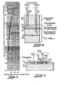
- Fig. 4 which is not drawn to scale, a schematic cross-sectional view of a semiconductor in the process of undergoing photolithograpy is illustrated. It is typical of a portion of an IGFET, but it is to be understood that the invention is not limited to IGFET's and may be used for other devices and in connection with other electron beam processing techniques.
- the device in Fig. 4 comprises a substrate 30 of semiconductor material, such as silicon or a composite material. This substrate is typically on the order of 400 microns thick. A thin layer of silicon dioxide (Si0 2 ) 31 overlies the substrate and it is approximately 0.01 to 0.05 microns thick.
- the polycrysta-- line silicon layer is approximately 0.3 microns thick and acts as a gate electrode.
- a thicker layer of silicon dioxide 34 overlies the polycrystaline silicon. It is approximately one micron thick and is used for masking, device isolation, surface passivation, or the like.
- a layer of photoresist 35 overlies the silicon dioxide layer 34 and is approximately three microns thick. Alternately, the photoresist may be of multiple layers.
- a bottom planarizing layer having portions that are two to three microns thick is used to overlay the topographical features of the underlying substrate being fabricated, such as the surface contours apparent in Fig. 2.
- a top imaging layer having a relatively uniform thickness of about 0.5 micron overlies the planarizing layer and is exposed in appropriate places by an electron beam to generate a photoresist mask.
- the local thickness of the photoresist coating may be determined based upon the known topography of the underlying substrate, as is evident from Fig. 2. Although not common, other variations may occur in the photoresist coating, e.g. density, depending upon the particular techniques or coating used, and these variations may be noted as necessary or desirable for use in correlating the accelerating voltage and amount of charge of the incident electron beam.
- the coated photoresist 30 is subjected to an incident electron beam or other ionizing radiation that is directed to trace a pattern on the photoresist and thereby expose it.
- the equipment and techniques for this exposure are well known, as are the techniques for controlling the deflection of the electron beam, its accelerating voltage, and the amount of charge of the incident electron beam, as it is deflected.
- Fig. 4 also illustrates the penetration of a 10 KeV incident electron beam 40 as compared to the penetration of a 25 KeV incident electron beam 41.
- the 10 KeV electron beam is illustrated as penetrating substantially the entire depth of the photoresist 20, but no more; the 25 the 25 KeV electron beam is illustrated as penetrating the photoresist 35, the passive silicon dioxide layer 34, the polycrystaline silicon layer 33, the active silicon dioxide layer 31, and into the underlying substrate 30.
- the differences between these two accelerating voltages and the resultant effects are best illustrated by the following hypothetical example.
- the relative degree of penetration of the electrons in terms of the energy absorbed in the three microns of photoresist may be quantified empirically as being roughly proportional to the ratio of the 16th power of the accelerating voltages. Assuming that a 10 KeV electron beam will fully expose photoresist that is three microns deep, a 25 KeV electron beam will penetrate approximately thirteen microns of photoresist, or four times as deep as the 10 KeV electron beam (based on Fig. 3). Therefore only (3/13) or 23 percent of the energy carried by the electrons is absorbed in the photoresist. The remaining 77 percent of the energy associated with the deeper penetrating electrons is wasted or dissipated in the underlying structures as illustrated in Fig. 3B, and this may result in undesirable damage.
- the amount of charge is also controlled so that the total energy of the electron beam (volts x charge) matches the energy that is absorbed by the photoresist for thorough exposure as the beam is deflected to trace a pattern on the photoresist.
- the amount of energy so absorbed may be readily determined and depends, in part, upon the density and thickness of the photoresist. Returning to our example, a 10 KeV electron beam with a dosage of 20 microcoulombs per cubic centimeter will impart 2 x 10 6 ergs per cubic centimeter for the three micron thickness of photoresist.
- the total energy is 5 x 10 6 ergs per cubic centimeter.
- the remaining 3.85 x 10 6 ergs of energy is dissipated in the underlying substrate where it may generate the unwanted defects discussed earlier, such as fixed positive charges and neutral traps.
- the fixed positive charges alter the threshold voltage of an IGFET, and if electrons become trapped in them or neutral traps during usage, the long term stability of the device will be impaired.
- the accelerating voltage of the electron beam is controlled and correlated to thickness variations in the photoresist as the electron beam traces a pattern so that the beam thoroughly penetrates the coated photoresist and dissipates substantially all of its energy therein, without significant penetration therethrough that might damage the underlying structure, particularly the gate and field insulators.
- the amount of charge of the projected electron beam so that the electron beam energy matches the amount of energy necessary to expose the photoresist, the electron beam thoroughly exposes the coated photoresist with no significant ionizing radiation damage to the underlying substrate.
- the accelerating voltage was usually increased without regard to excessive penetration of the underlying substrate or energy dissipation therein.
- the invention may be used to compensate for proximity effects, and to compensate for topographical variations resulting from the layered construction of the semiconductor. And, by appropriately controlling the voltage and the amount of charge of the projected electron beam to correlate the energy to variations in the photoresist thickness, the overall efficiency of the process is improved because a higher percentage of the energy of the electron beam is absorbed in the photoresist rather than being wasted in the underlying - layers.
- a substrate 50 is coated with a layer of photoresist 51.
- An electron beam 52 is deflected across the surface of the photoresist to trace the desired patterns, such as two adjacent strips.
- some electrons are reflected out of the target area, as illustrated by reference numeral 53.
- any reflected electrons are usually reabsorbed in the target area at adjacent locations, as illustrated by reflected beams 53A, 53B. It is those beams adjacent the perimeter of the. target area, such as beams 52B, 52C, 52D for which the full energy potential is not realized due to the escape of certain electrons from the target area.
- the electron beam voltage is tailored to the energy to be absorbed on a given layer thickness to minimize reflection and thereby optimize the electron energy absorption process. This improves efficiency and reduces the undesirable horizontal scattering of the electrons and any associated damage.
Landscapes
- Engineering & Computer Science (AREA)
- Chemical & Material Sciences (AREA)
- Nanotechnology (AREA)
- Physics & Mathematics (AREA)
- Crystallography & Structural Chemistry (AREA)
- General Physics & Mathematics (AREA)
- Manufacturing & Machinery (AREA)
- Condensed Matter Physics & Semiconductors (AREA)
- Mathematical Physics (AREA)
- Theoretical Computer Science (AREA)
- Analytical Chemistry (AREA)
- Electron Beam Exposure (AREA)
- Exposure And Positioning Against Photoresist Photosensitive Materials (AREA)
Priority Applications (1)
| Application Number | Priority Date | Filing Date | Title |
|---|---|---|---|
| AT85304167T ATE49678T1 (de) | 1984-06-14 | 1985-06-12 | Photoresistbelichtungsverfahren und geraet unter verwendung eines elektronenstrahls, dessen energie und ladung gesteuert werden. |
Applications Claiming Priority (2)
| Application Number | Priority Date | Filing Date | Title |
|---|---|---|---|
| US620510 | 1984-06-14 | ||
| US06/620,510 US4576884A (en) | 1984-06-14 | 1984-06-14 | Method and apparatus for exposing photoresist by using an electron beam and controlling its voltage and charge |
Publications (3)
| Publication Number | Publication Date |
|---|---|
| EP0165055A2 true EP0165055A2 (de) | 1985-12-18 |
| EP0165055A3 EP0165055A3 (en) | 1987-09-23 |
| EP0165055B1 EP0165055B1 (de) | 1990-01-17 |
Family
ID=24486252
Family Applications (1)
| Application Number | Title | Priority Date | Filing Date |
|---|---|---|---|
| EP85304167A Expired - Lifetime EP0165055B1 (de) | 1984-06-14 | 1985-06-12 | Photoresistbelichtungsverfahren und Gerät unter Verwendung eines Elektronenstrahls, dessen Energie und Ladung gesteuert werden |
Country Status (6)
| Country | Link |
|---|---|
| US (1) | US4576884A (de) |
| EP (1) | EP0165055B1 (de) |
| JP (1) | JPS6169123A (de) |
| AT (1) | ATE49678T1 (de) |
| CA (1) | CA1226075A (de) |
| DE (1) | DE3575496D1 (de) |
Families Citing this family (14)
| Publication number | Priority date | Publication date | Assignee | Title |
|---|---|---|---|---|
| US4981771A (en) * | 1984-11-02 | 1991-01-01 | Hitachi, Ltd. | Pattern fabricating method |
| US5141830A (en) * | 1989-09-20 | 1992-08-25 | Jeol Ltd. | Charged-particle beam lithography method |
| US5128849A (en) * | 1989-12-12 | 1992-07-07 | Optex Corpoataion | Optical disk structures for electron trapping optical memory media |
| US5195082A (en) * | 1989-12-12 | 1993-03-16 | Optex Corporation | Optical disk structures for electron trapping optical memory media |
| US5304441A (en) * | 1992-12-31 | 1994-04-19 | International Business Machines Corporation | Method of optimizing exposure of photoresist by patterning as a function of thermal modeling |
| JP2565121B2 (ja) * | 1993-12-14 | 1996-12-18 | 日本電気株式会社 | 電子線直接描画方法 |
| JP3431387B2 (ja) * | 1996-03-14 | 2003-07-28 | 株式会社東芝 | 露光強度分布表示方法とマスクパターン編集装置 |
| US6077762A (en) * | 1997-12-22 | 2000-06-20 | Vlsi Technology, Inc. | Method and apparatus for rapidly discharging plasma etched interconnect structures |
| US6093658A (en) * | 1997-12-22 | 2000-07-25 | Philips Electronics North America Corporation | Method for making reliable interconnect structures |
| US5928968A (en) | 1997-12-22 | 1999-07-27 | Vlsi Technology, Inc. | Semiconductor pressure transducer structures and methods for making the same |
| US6153531A (en) * | 1997-12-22 | 2000-11-28 | Philips Electronics North America Corporation | Method for preventing electrochemical erosion of interconnect structures |
| US5968710A (en) * | 1998-02-19 | 1999-10-19 | Micron Technology, Inc. | Controlled removal of electron beam curable coatings and articles formed thereby |
| US6472123B1 (en) | 2000-05-15 | 2002-10-29 | Micron Technology, Inc. | Multiple pass write method and reticle |
| JP4181561B2 (ja) * | 2005-05-12 | 2008-11-19 | 松下電器産業株式会社 | 半導体加工方法および加工装置 |
Family Cites Families (20)
| Publication number | Priority date | Publication date | Assignee | Title |
|---|---|---|---|---|
| GB1047390A (de) * | 1963-05-20 | 1900-01-01 | ||
| US3259898A (en) * | 1964-02-17 | 1966-07-05 | Lab For Electronics Inc | Doppler radar system |
| US3539401A (en) * | 1966-05-25 | 1970-11-10 | Matsushita Electric Industrial Co Ltd | Method of manufacturing mechano-electrical transducer |
| US3507709A (en) * | 1967-09-15 | 1970-04-21 | Hughes Aircraft Co | Method of irradiating dielectriccoated semiconductor bodies with low energy electrons |
| DE1614635A1 (de) * | 1967-10-23 | 1970-03-26 | Siemens Ag | Verfahren zum Herstellen von Fotolackmasken fuer Halbleiterzwecke |
| US3536547A (en) * | 1968-03-25 | 1970-10-27 | Bell Telephone Labor Inc | Plasma deposition of oxide coatings on silicon and electron bombardment of portions thereof to be etched selectively |
| US3737347A (en) * | 1970-02-26 | 1973-06-05 | Fairchild Camera Instr Co | Graded impurity profile in epitaxial films to improve integrated circuit performance |
| US3875416A (en) * | 1970-06-30 | 1975-04-01 | Texas Instruments Inc | Methods and apparatus for the production of semiconductor devices by electron-beam patterning and devices produced thereby |
| IE39611B1 (en) * | 1973-08-14 | 1978-11-22 | Siemens Ag | Improvements in or relating to two-phase charge coupled devices |
| US3950187A (en) * | 1974-11-15 | 1976-04-13 | Simulation Physics, Inc. | Method and apparatus involving pulsed electron beam processing of semiconductor devices |
| GB1534896A (en) * | 1975-05-19 | 1978-12-06 | Itt | Direct metal contact to buried layer |
| US4082958A (en) * | 1975-11-28 | 1978-04-04 | Simulation Physics, Inc. | Apparatus involving pulsed electron beam processing of semiconductor devices |
| US4232439A (en) * | 1976-11-30 | 1980-11-11 | Vlsi Technology Research Association | Masking technique usable in manufacturing semiconductor devices |
| JPS53121574A (en) * | 1977-03-31 | 1978-10-24 | Cho Lsi Gijutsu Kenkyu Kumiai | Electron beam exposing device |
| US4350866A (en) * | 1977-10-11 | 1982-09-21 | Fujitsu Limited | Discharge device and method for use in processing semiconductor devices |
| US4302530A (en) * | 1977-12-08 | 1981-11-24 | University Of Pennsylvania | Method for making substance-sensitive electrical structures by processing substance-sensitive photoresist material |
| US4348804A (en) * | 1978-07-12 | 1982-09-14 | Vlsi Technology Research Association | Method of fabricating an integrated circuit device utilizing electron beam irradiation and selective oxidation |
| US4383026A (en) * | 1979-05-31 | 1983-05-10 | Bell Telephone Laboratories, Incorporated | Accelerated particle lithographic processing and articles so produced |
| US4308586A (en) * | 1980-05-02 | 1981-12-29 | Nanometrics, Incorporated | Method for the precise determination of photoresist exposure time |
| JPS5851514A (ja) * | 1981-09-22 | 1983-03-26 | Toshiba Corp | ウエハ露光方法及びその装置 |
-
1984
- 1984-06-14 US US06/620,510 patent/US4576884A/en not_active Expired - Fee Related
-
1985
- 1985-06-12 DE DE8585304167T patent/DE3575496D1/de not_active Expired - Lifetime
- 1985-06-12 AT AT85304167T patent/ATE49678T1/de active
- 1985-06-12 CA CA000483787A patent/CA1226075A/en not_active Expired
- 1985-06-12 EP EP85304167A patent/EP0165055B1/de not_active Expired - Lifetime
- 1985-06-14 JP JP60128391A patent/JPS6169123A/ja active Pending
Also Published As
| Publication number | Publication date |
|---|---|
| CA1226075A (en) | 1987-08-25 |
| ATE49678T1 (de) | 1990-02-15 |
| EP0165055A3 (en) | 1987-09-23 |
| DE3575496D1 (de) | 1990-02-22 |
| US4576884A (en) | 1986-03-18 |
| EP0165055B1 (de) | 1990-01-17 |
| JPS6169123A (ja) | 1986-04-09 |
Similar Documents
| Publication | Publication Date | Title |
|---|---|---|
| EP0165055B1 (de) | Photoresistbelichtungsverfahren und Gerät unter Verwendung eines Elektronenstrahls, dessen Energie und Ladung gesteuert werden | |
| US4420872A (en) | Method of manufacturing a semiconductor device | |
| US3747203A (en) | Methods of manufacturing a semiconductor device | |
| US6180487B1 (en) | Selective thinning of barrier oxide through masked SIMOX implant | |
| US5024965A (en) | Manufacturing high speed low leakage radiation hardened CMOS/SOI devices | |
| US3558366A (en) | Metal shielding for ion implanted semiconductor device | |
| US3390019A (en) | Method of making a semiconductor by ionic bombardment | |
| Aitken | 1/spl mu/m MOSFET VLSI technology. VIII. Radiation effects | |
| US4716451A (en) | Semiconductor device with internal gettering region | |
| US4096509A (en) | MNOS memory transistor having a redeposited silicon nitride gate dielectric | |
| US5705441A (en) | Ion implant silicon nitride mask for a silicide free contact region in a self aligned silicide process | |
| US4900688A (en) | Pseudo uniphase charge coupled device fabrication by self-aligned virtual barrier and virtual gate formation | |
| EP0273702A2 (de) | Technik um Metall-Oxid-Silizium Bauelemente gegen Strahlungen abzuhärten | |
| US3688389A (en) | Insulated gate type field effect semiconductor device having narrow channel and method of fabricating same | |
| US4948741A (en) | Polysilicon photoconductor for integrated circuits | |
| CA1043474A (en) | Method of high current ion implantation | |
| US5384268A (en) | Charge damage free implantation by introduction of a thin conductive layer | |
| JP3311759B2 (ja) | スクリーン構造を有する集積回路およびその製造方法 | |
| KR960005943A (ko) | 반도체 소자의 격리방법 | |
| US4821091A (en) | Polysilicon photoconductor for integrated circuits | |
| US5219766A (en) | Semiconductor device having a radiation resistance and method for manufacturing same | |
| US5284793A (en) | Method of manufacturing radiation resistant semiconductor device | |
| Lukaszek | Wafer charging damage in IC process equipment | |
| US6989310B2 (en) | Process and installation for doping an etched pattern of resistive elements | |
| JPS62174915A (ja) | 半導体装置の製造方法 |
Legal Events
| Date | Code | Title | Description |
|---|---|---|---|
| PUAI | Public reference made under article 153(3) epc to a published international application that has entered the european phase |
Free format text: ORIGINAL CODE: 0009012 |
|
| AK | Designated contracting states |
Designated state(s): AT BE CH DE FR GB IT LI LU NL SE |
|
| PUAL | Search report despatched |
Free format text: ORIGINAL CODE: 0009013 |
|
| AK | Designated contracting states |
Kind code of ref document: A3 Designated state(s): AT BE CH DE FR GB IT LI LU NL SE |
|
| 17P | Request for examination filed |
Effective date: 19880316 |
|
| 17Q | First examination report despatched |
Effective date: 19890118 |
|
| GRAA | (expected) grant |
Free format text: ORIGINAL CODE: 0009210 |
|
| AK | Designated contracting states |
Kind code of ref document: B1 Designated state(s): AT BE CH DE FR GB IT LI LU NL SE |
|
| PG25 | Lapsed in a contracting state [announced via postgrant information from national office to epo] |
Ref country code: SE Effective date: 19900117 Ref country code: BE Effective date: 19900117 Ref country code: AT Effective date: 19900117 |
|
| REF | Corresponds to: |
Ref document number: 49678 Country of ref document: AT Date of ref document: 19900215 Kind code of ref document: T |
|
| REF | Corresponds to: |
Ref document number: 3575496 Country of ref document: DE Date of ref document: 19900222 |
|
| ITF | It: translation for a ep patent filed | ||
| ET | Fr: translation filed | ||
| PGFP | Annual fee paid to national office [announced via postgrant information from national office to epo] |
Ref country code: FR Payment date: 19900522 Year of fee payment: 6 |
|
| PGFP | Annual fee paid to national office [announced via postgrant information from national office to epo] |
Ref country code: GB Payment date: 19900608 Year of fee payment: 6 |
|
| PGFP | Annual fee paid to national office [announced via postgrant information from national office to epo] |
Ref country code: DE Payment date: 19900620 Year of fee payment: 6 |
|
| ITTA | It: last paid annual fee | ||
| PG25 | Lapsed in a contracting state [announced via postgrant information from national office to epo] |
Ref country code: LU Free format text: LAPSE BECAUSE OF NON-PAYMENT OF DUE FEES Effective date: 19900630 |
|
| PGFP | Annual fee paid to national office [announced via postgrant information from national office to epo] |
Ref country code: NL Payment date: 19900630 Year of fee payment: 6 |
|
| PGFP | Annual fee paid to national office [announced via postgrant information from national office to epo] |
Ref country code: CH Payment date: 19900827 Year of fee payment: 6 |
|
| PLBE | No opposition filed within time limit |
Free format text: ORIGINAL CODE: 0009261 |
|
| STAA | Information on the status of an ep patent application or granted ep patent |
Free format text: STATUS: NO OPPOSITION FILED WITHIN TIME LIMIT |
|
| 26N | No opposition filed | ||
| REG | Reference to a national code |
Ref country code: CH Ref legal event code: PFA Free format text: MCNC |
|
| ITPR | It: changes in ownership of a european patent |
Owner name: CAMBIO RAGIONE SOCIALE;M/CNC |
|
| REG | Reference to a national code |
Ref country code: FR Ref legal event code: CD |
|
| PG25 | Lapsed in a contracting state [announced via postgrant information from national office to epo] |
Ref country code: GB Effective date: 19910612 |
|
| NLT1 | Nl: modifications of names registered in virtue of documents presented to the patent office pursuant to art. 16 a, paragraph 1 |
Owner name: MCNC TE TRIANGLE PARK, NORTH CAROLINA, VER. ST. V. |
|
| PG25 | Lapsed in a contracting state [announced via postgrant information from national office to epo] |
Ref country code: LI Effective date: 19910630 Ref country code: CH Effective date: 19910630 |
|
| PG25 | Lapsed in a contracting state [announced via postgrant information from national office to epo] |
Ref country code: NL Effective date: 19920101 |
|
| GBPC | Gb: european patent ceased through non-payment of renewal fee | ||
| NLV4 | Nl: lapsed or anulled due to non-payment of the annual fee | ||
| PG25 | Lapsed in a contracting state [announced via postgrant information from national office to epo] |
Ref country code: FR Effective date: 19920228 |
|
| REG | Reference to a national code |
Ref country code: CH Ref legal event code: PL |
|
| PG25 | Lapsed in a contracting state [announced via postgrant information from national office to epo] |
Ref country code: DE Effective date: 19920401 |
|
| REG | Reference to a national code |
Ref country code: FR Ref legal event code: ST |