EP0165149A1 - Filterkontakt und seine Verwendung bei elektrischen Steckverbindern - Google Patents
Filterkontakt und seine Verwendung bei elektrischen Steckverbindern Download PDFInfo
- Publication number
- EP0165149A1 EP0165149A1 EP85400993A EP85400993A EP0165149A1 EP 0165149 A1 EP0165149 A1 EP 0165149A1 EP 85400993 A EP85400993 A EP 85400993A EP 85400993 A EP85400993 A EP 85400993A EP 0165149 A1 EP0165149 A1 EP 0165149A1
- Authority
- EP
- European Patent Office
- Prior art keywords
- electrode
- varistor
- filter
- contact
- tubular
- Prior art date
- Legal status (The legal status is an assumption and is not a legal conclusion. Google has not performed a legal analysis and makes no representation as to the accuracy of the status listed.)
- Granted
Links
- 229910052751 metal Inorganic materials 0.000 claims abstract description 10
- 239000002184 metal Substances 0.000 claims abstract description 10
- 239000002003 electrode paste Substances 0.000 claims abstract description 5
- 239000011248 coating agent Substances 0.000 claims abstract description 4
- 238000000576 coating method Methods 0.000 claims abstract description 4
- 229910000679 solder Inorganic materials 0.000 claims description 7
- XLOMVQKBTHCTTD-UHFFFAOYSA-N Zinc monoxide Chemical compound [Zn]=O XLOMVQKBTHCTTD-UHFFFAOYSA-N 0.000 description 4
- 239000000203 mixture Substances 0.000 description 3
- 230000008021 deposition Effects 0.000 description 2
- 239000011787 zinc oxide Substances 0.000 description 2
- 230000015556 catabolic process Effects 0.000 description 1
- 239000000919 ceramic Substances 0.000 description 1
- 230000001419 dependent effect Effects 0.000 description 1
- 238000001035 drying Methods 0.000 description 1
- 238000010438 heat treatment Methods 0.000 description 1
- 238000012423 maintenance Methods 0.000 description 1
- 239000000155 melt Substances 0.000 description 1
- 238000000034 method Methods 0.000 description 1
- 244000045947 parasite Species 0.000 description 1
- 230000003071 parasitic effect Effects 0.000 description 1
- 238000007650 screen-printing Methods 0.000 description 1
- 229910052709 silver Inorganic materials 0.000 description 1
- 239000004332 silver Substances 0.000 description 1
- 238000005245 sintering Methods 0.000 description 1
- 238000009987 spinning Methods 0.000 description 1
- 230000007704 transition Effects 0.000 description 1
- 229910000859 α-Fe Inorganic materials 0.000 description 1
Images
Classifications
-
- H—ELECTRICITY
- H01—ELECTRIC ELEMENTS
- H01R—ELECTRICALLY-CONDUCTIVE CONNECTIONS; STRUCTURAL ASSOCIATIONS OF A PLURALITY OF MUTUALLY-INSULATED ELECTRICAL CONNECTING ELEMENTS; COUPLING DEVICES; CURRENT COLLECTORS
- H01R13/00—Details of coupling devices of the kinds covered by groups H01R12/70 or H01R24/00 - H01R33/00
- H01R13/66—Structural association with built-in electrical component
- H01R13/719—Structural association with built-in electrical component specially adapted for high frequency, e.g. with filters
- H01R13/7197—Structural association with built-in electrical component specially adapted for high frequency, e.g. with filters with filters integral with or fitted onto contacts, e.g. tubular filters
-
- H—ELECTRICITY
- H01—ELECTRIC ELEMENTS
- H01C—RESISTORS
- H01C7/00—Non-adjustable resistors formed as one or more layers or coatings; Non-adjustable resistors made from powdered conducting material or powdered semi-conducting material with or without insulating material
- H01C7/10—Non-adjustable resistors formed as one or more layers or coatings; Non-adjustable resistors made from powdered conducting material or powdered semi-conducting material with or without insulating material voltage responsive, i.e. varistors
- H01C7/102—Varistor boundary, e.g. surface layers
-
- H—ELECTRICITY
- H03—ELECTRONIC CIRCUITRY
- H03H—IMPEDANCE NETWORKS, e.g. RESONANT CIRCUITS; RESONATORS
- H03H1/00—Constructional details of impedance networks whose electrical mode of operation is not specified or applicable to more than one type of network
- H03H1/0007—Constructional details of impedance networks whose electrical mode of operation is not specified or applicable to more than one type of network of radio frequency interference filters
-
- H—ELECTRICITY
- H01—ELECTRIC ELEMENTS
- H01R—ELECTRICALLY-CONDUCTIVE CONNECTIONS; STRUCTURAL ASSOCIATIONS OF A PLURALITY OF MUTUALLY-INSULATED ELECTRICAL CONNECTING ELEMENTS; COUPLING DEVICES; CURRENT COLLECTORS
- H01R13/00—Details of coupling devices of the kinds covered by groups H01R12/70 or H01R24/00 - H01R33/00
- H01R13/648—Protective earth or shield arrangements on coupling devices, e.g. anti-static shielding
- H01R13/658—High frequency shielding arrangements, e.g. against EMI [Electro-Magnetic Interference] or EMP [Electro-Magnetic Pulse]
- H01R13/6581—Shield structure
- H01R13/6585—Shielding material individually surrounding or interposed between mutually spaced contacts
- H01R13/6588—Shielding material individually surrounding or interposed between mutually spaced contacts with through openings for individual contacts
Definitions
- the present invention relates to a filter contact comprising an electrical contact in the form of a metal rod, surrounded by a tubular filter element, provided with a first electrode on its external face and a second electrode on its internal face, this the second electrode being electrically connected to the electrical contact, the two electrodes being isolated from one another.
- Such filter contacts are particularly useful in electrical connectors.
- a filter contact of this type is described in French patent 2 185 879.
- the filter contacts described in this application are particularly intended for attenuation of high frequency waves.
- the filter used consists of a ceramic tubular element in which is housed a ferrite tubular element. An LC type filter is thus obtained having a cut-off frequency dependent on the value of these elements.
- filter elements make it possible to suppress the HF waves capable of modulating an analog signal conveyed by the electrical contact, they are generally ill-suited to the protection of digital signals against parasitic pulses of various origins, presenting a high surge in a random manner . Such parasites are likely to modify the content of the message transmitted in digital form, which can cause errors in the received signal.
- the filter contact according to the invention is characterized in that the filter element of tubular shape is constituted by a tubular varistor whose second electrode extends at least on one of its lateral faces which has a rounded area of a shape such that the coating of the electrode paste, known per se, in this zone, produces a deposit of substantially constant thickness.
- the filter contact according to the invention is characterized in that the second electrode is electrically connected to the contact by a solder, produced in the region of the lateral face of the varistor having a rounded shape.
- the first electrode of such a filter contact which is arranged on the external face of the varistor, is connected to the metal body of the connector and / or to ground.
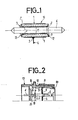
- FIG. 1 shows a sectional view of a filter contact according to the invention.
- This filter contact is essentially composed of an electrical contact 6 and a varistor 10.
- This varistor 10 is tubular in shape and surrounds the electrical contact 6.
- This varistor 10 comprises a body 2 having a non-linear resistance with a threshold of tension V o , well known under the name varistor.
- This tubular body 2 is surrounded externally by a cylindrical electrode 1 and internally by an equally cylindrical electrode 11.
- This internal electrode 11 is extended on the lateral faces of the tubular varistor and completely covers said lateral faces, in the example shown here. -above.
- This internal electrode 11 has a rounded part 7 which follows the substantially identical rounded shape of the lateral faces of the body 2 of the varistor 10.
- this internal electrode 11 can continue on the external face of the tube forming the varistor 10.
- the electrodes 1 and 11 will be arranged at a distance sufficient to avoid any risk of possible breakdown between the electrodes.
- the lateral face 13 of the varistor 10 is soldered to the electrical contact 6.
- the solder 3 makes both the electrical contact and the mechanical maintenance between the varistor and the electrical contact 6.
- solder 3 the lateral face 12 of the varistor 10.
- the external electrode 1 of the varistor is connected by a solder 5 to a ground plane 4.
- the varistor element proper constituting the body 2 of this varistor 10 may be produced, for example according to the indications given in French patents 2,363,171 or 2,475,791. In particular, the latter specifies the thickness to be given to the varistor element according to the threshold voltage V 0 at which it is desired to see this element toggle.
- this varistor element 10 will be produced from a composition based on zinc oxide ZnO well known to those skilled in the art.
- the process for producing tubular varistors consists in spinning a dough of the composition determined on a spindle so as to obtain a hollow tube which is cut after drying into elements of desired length and then sintered at the appropriate temperature.
- the electrodes are deposited on this tubular element in the form of a silver-based paste for screen printing.
- the deposition of the internal electrode must be carried out with care. Indeed, if one wants to be able to easily weld this electrode with contact 6 with good electrical contact, it is necessary for this internal electrode 11 to extend slightly or completely over at least one of the lateral faces 12, 13 of the tubular varistor 10. For this, it was found that it was necessary to round the internal edges of the varistor, so as to remove any angle 10 at the transition between the internal face of the body of the varistor 2 and the lateral faces 12 and 13.
- the exact shape of the rounding to be given is determined in practice by a person skilled in the art by simple routine manipulations, depending on the nature of the electrode paste used as well as the composition of the varistor body 2.
- This rounding will have a shape such that, during the deposition of the electrode paste, by coating, an internal electrode 11 of substantially constant thickness is obtained between the internal part of the varistor up to the end at least from the side face 12 and / or 13.
- FIG 2 there is shown a partial sectional view of a connector using a contact according to the invention.
- This connector 15 comprises a metal body 16 in which an electrical block 17 is housed, extended by a flexible rubber grommet 18.
- the electrical contact 6, provided with its varistor 10 is introduced into the corresponding housing 19 of the insulating block 17
- This electrical contact 6 comes to bear by its front part 20 against a corresponding stop of the insulating block 17.
- the assembly is capped by a metal plate 4 pierced with holes of diameter substantially equal, apart from play, to the outside diameter of the varistor 10, then solder preforms 3 are placed around each electrical contact 6 and a solder preform 8 at the end of the metal plate 4.
Landscapes
- Engineering & Computer Science (AREA)
- Microelectronics & Electronic Packaging (AREA)
- Physics & Mathematics (AREA)
- Electromagnetism (AREA)
- Thermistors And Varistors (AREA)
Applications Claiming Priority (2)
| Application Number | Priority Date | Filing Date | Title |
|---|---|---|---|
| FR8408251 | 1984-05-25 | ||
| FR8408251A FR2565041B1 (fr) | 1984-05-25 | 1984-05-25 | Contact filtre et son utilisation dans les connecteurs electriques |
Publications (2)
| Publication Number | Publication Date |
|---|---|
| EP0165149A1 true EP0165149A1 (de) | 1985-12-18 |
| EP0165149B1 EP0165149B1 (de) | 1988-05-18 |
Family
ID=9304414
Family Applications (1)
| Application Number | Title | Priority Date | Filing Date |
|---|---|---|---|
| EP85400993A Expired EP0165149B1 (de) | 1984-05-25 | 1985-05-21 | Filterkontakt und seine Verwendung bei elektrischen Steckverbindern |
Country Status (4)
| Country | Link |
|---|---|
| US (1) | US4646037A (de) |
| EP (1) | EP0165149B1 (de) |
| DE (1) | DE3562846D1 (de) |
| FR (1) | FR2565041B1 (de) |
Cited By (1)
| Publication number | Priority date | Publication date | Assignee | Title |
|---|---|---|---|---|
| EP0288546A4 (de) * | 1986-11-03 | 1989-02-22 | Amphenol Corp | Elektrischer kontakt mit einschwingungsvorgängenunterdrückung. |
Families Citing this family (8)
| Publication number | Priority date | Publication date | Assignee | Title |
|---|---|---|---|---|
| GB8621429D0 (en) * | 1986-09-05 | 1987-01-14 | Raychem Pontoise Sa | Circuit protection device |
| US4707049A (en) * | 1986-11-03 | 1987-11-17 | Amphenol Corporation | Electrical connector having transient protection |
| CA1292502C (en) * | 1987-01-26 | 1991-11-26 | James Edward Anderson | Packaged solid state primary surge protector |
| US4939619A (en) * | 1987-01-26 | 1990-07-03 | Northern Telecom Limited | Packaged solid-state surge protector |
| US5167537A (en) * | 1991-05-10 | 1992-12-01 | Amphenol Corporation | High density mlv contact assembly |
| US5500629A (en) * | 1993-09-10 | 1996-03-19 | Meyer Dennis R | Noise suppressor |
| US5999398A (en) * | 1998-06-24 | 1999-12-07 | Avx Corporation | Feed-through filter assembly having varistor and capacitor structure |
| FR2798784B1 (fr) * | 1999-09-17 | 2002-01-11 | Francois Girard | Dispositif de protection contre les surtensions |
Citations (4)
| Publication number | Priority date | Publication date | Assignee | Title |
|---|---|---|---|---|
| US3002162A (en) * | 1958-11-20 | 1961-09-26 | Allen Bradley Co | Multiple terminal filter connector |
| US3435387A (en) * | 1965-09-01 | 1969-03-25 | Allen Bradley Co | Solderless mounting filter connection |
| US3711794A (en) * | 1971-10-21 | 1973-01-16 | Gen Electric | Surge suppression transmission means |
| US3840841A (en) * | 1973-06-13 | 1974-10-08 | Bendix Corp | Electrical connector having rf filter |
-
1984
- 1984-05-25 FR FR8408251A patent/FR2565041B1/fr not_active Expired
-
1985
- 1985-05-21 EP EP85400993A patent/EP0165149B1/de not_active Expired
- 1985-05-21 DE DE8585400993T patent/DE3562846D1/de not_active Expired
- 1985-05-22 US US06/736,844 patent/US4646037A/en not_active Expired - Fee Related
Patent Citations (4)
| Publication number | Priority date | Publication date | Assignee | Title |
|---|---|---|---|---|
| US3002162A (en) * | 1958-11-20 | 1961-09-26 | Allen Bradley Co | Multiple terminal filter connector |
| US3435387A (en) * | 1965-09-01 | 1969-03-25 | Allen Bradley Co | Solderless mounting filter connection |
| US3711794A (en) * | 1971-10-21 | 1973-01-16 | Gen Electric | Surge suppression transmission means |
| US3840841A (en) * | 1973-06-13 | 1974-10-08 | Bendix Corp | Electrical connector having rf filter |
Non-Patent Citations (1)
| Title |
|---|
| MACHINE DESIGN, vol. 52, no. 7, avril 1980, pages 135-136, Cleveland, Ohio, US; P. DOBROGOWSKI: "Filtering EMI with connectors" * |
Cited By (1)
| Publication number | Priority date | Publication date | Assignee | Title |
|---|---|---|---|---|
| EP0288546A4 (de) * | 1986-11-03 | 1989-02-22 | Amphenol Corp | Elektrischer kontakt mit einschwingungsvorgängenunterdrückung. |
Also Published As
| Publication number | Publication date |
|---|---|
| DE3562846D1 (en) | 1988-06-23 |
| US4646037A (en) | 1987-02-24 |
| FR2565041B1 (fr) | 1986-08-22 |
| EP0165149B1 (de) | 1988-05-18 |
| FR2565041A1 (fr) | 1985-11-29 |
Similar Documents
| Publication | Publication Date | Title |
|---|---|---|
| FR2822543A1 (fr) | Detecteur de temperature | |
| EP0165149B1 (de) | Filterkontakt und seine Verwendung bei elektrischen Steckverbindern | |
| EP0260173B1 (de) | Piezoelektrische Hydrophone mit verbesserter Empfindlichkeit | |
| EP0096611B1 (de) | Hochfrequenter piezoelektrischer Schwinger und Herstellungsverfahren | |
| FR2781566A1 (fr) | Capteur de temperature et procede de fabrication de celui-ci | |
| EP0649181A1 (de) | Antenne für tragbares Funkgerät, Verfahren zur Herstellung einer derartigen Antenne und tragbares Funkgerät mit einer derartigen Antenne | |
| EP0402251A1 (de) | Transkutane Verbindungseinrichtung | |
| EP0544367B1 (de) | Kapazitiver Sensor mit leitender Frontseite, zur Bildung einer Kondensatorarmatur und einem mineralisierten abgeschirmten Koaxialkabel | |
| FR2835609A1 (fr) | Capteur de temperature a thermistance et son procede de fabrication | |
| EP3644450A1 (de) | Elektrischer anschluss, der eine vielzahl von rückhalteorgangen umfasst | |
| FR2597266A1 (fr) | Antenne a large bande | |
| FR2489066A1 (fr) | Bougies incandescentes pour moteurs diesel | |
| EP4007521A1 (de) | Vorrichtung zum bestimmen des elektrischen potenzials des gehirns | |
| EP0308935A1 (de) | Armbandantenne für Radioempfänger, der in eine Uhr eingebaut ist | |
| EP0262005B1 (de) | Herstellungsverfahren für eine bimetallische Mittelelektrode mit einem Platinstift für Zündkerze und Elektrode, hergestellt nach diesem Verfahren | |
| FR2891952A3 (fr) | Adaptateur pour transmission de signal haute frequence | |
| FR2734970A1 (fr) | Ligne de liaison electrique coaxiale | |
| EP1607761A1 (de) | Multifrequenz-Stromeinspeisung und Spule und NMR-Spektrometer mit einer solchen Stromeinspeisung | |
| EP0076735A1 (de) | Apparat zum Aufbringen von wärmeschmelzbarem Leim | |
| FR2528617A1 (fr) | Circuit resistant en couche epaisse avec fusible incorpore | |
| FR2524031A1 (fr) | Perfectionnements aux dispositifs d'ancrage destines a etre enfonces dans le sol | |
| FR3018003B1 (fr) | Systeme d'adaptation d'impedance et systeme de contact avec un tel systeme d'adaptation d'impedance | |
| FR2565040A1 (fr) | Connecteur muni de contacts filtres et son procede de fabrication | |
| EP0442411B1 (de) | Konische Feder für einen elektrischen Kontakt | |
| EP0298819B1 (de) | Elektrischer Steckverbinder |
Legal Events
| Date | Code | Title | Description |
|---|---|---|---|
| PUAI | Public reference made under article 153(3) epc to a published international application that has entered the european phase |
Free format text: ORIGINAL CODE: 0009012 |
|
| AK | Designated contracting states |
Designated state(s): DE FR GB NL |
|
| 17P | Request for examination filed |
Effective date: 19851228 |
|
| RAP1 | Party data changed (applicant data changed or rights of an application transferred) |
Owner name: COMPAGNIE EUROPEENNE DE COMPOSANTS ELECTRONIQUES L |
|
| 17Q | First examination report despatched |
Effective date: 19860828 |
|
| GRAA | (expected) grant |
Free format text: ORIGINAL CODE: 0009210 |
|
| AK | Designated contracting states |
Kind code of ref document: B1 Designated state(s): DE FR GB |
|
| GBT | Gb: translation of ep patent filed (gb section 77(6)(a)/1977) | ||
| REF | Corresponds to: |
Ref document number: 3562846 Country of ref document: DE Date of ref document: 19880623 |
|
| PLBE | No opposition filed within time limit |
Free format text: ORIGINAL CODE: 0009261 |
|
| STAA | Information on the status of an ep patent application or granted ep patent |
Free format text: STATUS: NO OPPOSITION FILED WITHIN TIME LIMIT |
|
| 26N | No opposition filed | ||
| PGFP | Annual fee paid to national office [announced via postgrant information from national office to epo] |
Ref country code: DE Payment date: 19910419 Year of fee payment: 7 |
|
| PGFP | Annual fee paid to national office [announced via postgrant information from national office to epo] |
Ref country code: GB Payment date: 19910423 Year of fee payment: 7 |
|
| PGFP | Annual fee paid to national office [announced via postgrant information from national office to epo] |
Ref country code: FR Payment date: 19910524 Year of fee payment: 7 |
|
| PG25 | Lapsed in a contracting state [announced via postgrant information from national office to epo] |
Ref country code: GB Effective date: 19920521 |
|
| GBPC | Gb: european patent ceased through non-payment of renewal fee |
Effective date: 19920521 |
|
| PG25 | Lapsed in a contracting state [announced via postgrant information from national office to epo] |
Ref country code: FR Effective date: 19930129 |
|
| PG25 | Lapsed in a contracting state [announced via postgrant information from national office to epo] |
Ref country code: DE Effective date: 19930202 |
|
| REG | Reference to a national code |
Ref country code: FR Ref legal event code: ST |