EP0165548B1 - Petit appareil électronique comportant un système d'entrée optique - Google Patents
Petit appareil électronique comportant un système d'entrée optique Download PDFInfo
- Publication number
- EP0165548B1 EP0165548B1 EP85107239A EP85107239A EP0165548B1 EP 0165548 B1 EP0165548 B1 EP 0165548B1 EP 85107239 A EP85107239 A EP 85107239A EP 85107239 A EP85107239 A EP 85107239A EP 0165548 B1 EP0165548 B1 EP 0165548B1
- Authority
- EP
- European Patent Office
- Prior art keywords
- data
- photosensor
- register
- photosensors
- section
- Prior art date
- Legal status (The legal status is an assumption and is not a legal conclusion. Google has not performed a legal analysis and makes no representation as to the accuracy of the status listed.)
- Expired
Links
Images





Classifications
-
- G—PHYSICS
- G06—COMPUTING OR CALCULATING; COUNTING
- G06F—ELECTRIC DIGITAL DATA PROCESSING
- G06F3/00—Input arrangements for transferring data to be processed into a form capable of being handled by the computer; Output arrangements for transferring data from processing unit to output unit, e.g. interface arrangements
- G06F3/01—Input arrangements or combined input and output arrangements for interaction between user and computer
- G06F3/03—Arrangements for converting the position or the displacement of a member into a coded form
- G06F3/041—Digitisers, e.g. for touch screens or touch pads, characterised by the transducing means
- G06F3/042—Digitisers, e.g. for touch screens or touch pads, characterised by the transducing means by opto-electronic means
-
- G—PHYSICS
- G04—HOROLOGY
- G04G—ELECTRONIC TIME-PIECES
- G04G21/00—Input or output devices integrated in time-pieces
- G04G21/08—Touch switches specially adapted for time-pieces
-
- G—PHYSICS
- G06—COMPUTING OR CALCULATING; COUNTING
- G06F—ELECTRIC DIGITAL DATA PROCESSING
- G06F3/00—Input arrangements for transferring data to be processed into a form capable of being handled by the computer; Output arrangements for transferring data from processing unit to output unit, e.g. interface arrangements
- G06F3/01—Input arrangements or combined input and output arrangements for interaction between user and computer
- G06F3/03—Arrangements for converting the position or the displacement of a member into a coded form
- G06F3/041—Digitisers, e.g. for touch screens or touch pads, characterised by the transducing means
- G06F3/042—Digitisers, e.g. for touch screens or touch pads, characterised by the transducing means by opto-electronic means
- G06F3/0421—Digitisers, e.g. for touch screens or touch pads, characterised by the transducing means by opto-electronic means by interrupting or reflecting a light beam, e.g. optical touch-screen
Definitions
- This invention relates to a small electronic apparatus with an optical input device and, more particularly, to a small electronic apparatus such as a digital wristwatch with a calculation function for optically entering input data such as numerical values and characters.
- an external input means comprising a ten key pad or letter keys on the surface of the wristwatch case.
- a large mounting space is required for such an external input means.
- the waterproof structure of the wristwatch is complicated. Therefore, the conventional external input means cannot be suitably incorporated in a small electronic watch such as a wristwatch.
- a conventional electronic wristwatch wherein a plurality of transparent touch electrodes are formed on the front surface of a protection glass plate for covering a display device.
- a switch input is performed.
- the transparent electrodes are formed on the protection glass plate, which are easily damaged, thereby disconnecting the transparent electrodes. Since a number of electrodes are exposed to the outer atmosphere, static electricity and noise tend to be mixed in an LSI (large scale integrated circuit) of the wristwatch, resulting in circuit damage and operation failure.
- LSI large scale integrated circuit
- US-A-4 345 248 relates to an apparatus wherein the liquid display device is used as an input device.
- Array electrodes and row electroces are formed in a matrix pattern on a transparent substrate, and display electrodes, switching elements, and light-sensitive elements are formed at the intersections of the row and column electrodes.
- Drive signals are supplied to the row and column electrodes so as to drive the switchingiatas, thereby causing the display electrodes to display information.
- the outputs of the row and column electrodes are detected in order to sense which of the light-sensitive electrodes light enters.
- the display of information and the detection of the outputs of the row and column electrodes are effected on the time-divisional basis.
- the position at which the light input is performed is detected when a light pen is brought into contact with the liquid crystal display device, and a figure or the like is input in accordance with the detected position.
- an input operation is performed through utilization of the light-sensitive elements, whereas the outputs of the light-sensitive elements are always detected during an input mode. Therefore, if light emitted from a device or the like other than the light pen undesirably enters the apparatus through the liquid crystal display device during the input mode, this may cause malfunctioning of the apparatus. Further, when the light pen is positioned such that a specific one of the light-sensitive elements is irraidated with the light emitted from the light pen, another light-sensitive element may be irradiated with the light, thereby causing malfunction of the apparatus. To prevent the malfunction, the light pen should be carefully positioned, with the result that the operational efficiency of the apparatus is degraded.
- US-A-4 139 837 discloses a manual information entry device wherein a plurality of touch electrodes are provided on the surface of the glas of the wristwatch, and, when a letter is traced by a human finger on the touch electrodes, the letter is traced as detected such that predetermined data is input.
- a small electronic apparatus in particular on the scale of a human hand or finger, including an optical input device, comprising:
- the small electronic apparatus of the present invention employs structures wherein a photosensor is arranged in the apparatus case such that it opposes the light-transmitting member of the apparatus case, wherein a touch switch is provided on the upper surface of the light-transmitting member and wherein detecting means are operative such that the output of the photosensor is detected only when a human finger touches the touch switch. Therefore, even if an object approaches the light-transmitting member such that light entering the photosensor is obstructed thereby, the detecting means will not detect the obstructions as switching having been performed. Thus, if the light entering one photosensor is undesirably obstructed by a human finger while approaching another photosensor to touch the same, the detection will not be effected. As a result, malfunctioning of the apparatus can be advantageously prevented from being caused by an object obstructing the light entering the photosensor. Further, it is not necessary to provide a switch for inputting start of a detecting operation.
- a transparent protection glass plate 3 is pressed and fixed at an upper opening of a wristwatch case 1 to cover a liquid crystal device 2.
- a transparent electrode 4 constituting a touch switch is formed on the upper surface of the glass plate 3.
- the electrode 4 has a size substantially corresponding to the display screen area of the device 2.
- One end of the electrode 4 extends below the lower surface of the glass plate 3 and is electrically connected to a printed circuit board 6 through an interconnector 5.
- the wristwatch case serves as one electrode. Under a condition wherein the user's wrist is in contact with a lower cover 7, when a finger of his hand is brought into contact with the electrode 4, the wristwatch is electrically connected to the transparent electrode through a human resistor.
- the device 2 has a segment electrode structure and can display the following contents in accordance with its electrode pattern.
- a digital display section 2A as an upper portion of the display screen comprises 8-segment display elements for displaying time, and registered and calculated data in the digital form.
- a function display section 2B as a lower portion of the display screen specifies the functions of the calculation keys and key positions.
- the section 2B displays numbers 0 to 9, a decimal point, operators (x, -, +, -) of four arithmetic calculations, and an equal mark in a 4 x 4 matrix.
- the section 2B also has matrix lines for dividing the section 2B into 16 portions.
- the device 2 is electrically connected to the board 6 through interconnectors 8.
- the input elements (to be referred to as photosensors hereinafter) In can be constituted by monocrystalline silicon phototransistors, amorphous silicon phototransistors, or amorphous photoconductive cells. Outputs from the photosensors are obtained as changes in voltages, currents or resistances in accordance with light-receiving levels.
- the photosensors In are made of amorphous silicon semiconductor instead of monocrystalline silicon semiconductor since amorphous silicon can be formed in a small size. In practice, each photosensor is a square having a side of 0.2 mm 2 or less.
- the photosensors In have a size which cannot be visually identified with clarity and overlapping the display contents of the section 2B.
- the photosensors In are electrically connected to the board 6 through the interconnector 5.
- Reference numeral 9 denotes an LSI (large scale integrated circuit) mounted on the board 6.
- a mode changing key Sm for selecting the timepiece mode or the calculator mode and an all clear key AC in the calculator mode are arranged at two side walls of the electronic wristwatch, respectively.
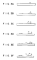
- Fig. 3 shows the steps in manufacturing the photosensors In.
- a transparent conductive film I of indium oxide or the like is formed by deposition or sputtering on the lower surface of the glass plate 3 (Fig. 3A).
- the film I is patterned (Fig. 3B).
- An amorphous silicon film m is formed by deposition or sputtering on the entire surface of the glass plate 3 (Fig. 3C).
- the amorphous silicon film m is patterned (Fig. 3D).
- An electrode film n is formed to cover the entire surface (Fig. 3E) and is patterned to obtain the photosensors In (Fig. 3F).
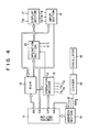
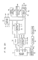
- a control section 11 constituted by a ROM (read-only memory) stores a microprogram for controlling the overall operation of the wristwatch and for generating parallel microinstructions AD, DA, OP and NA (to be described later).
- the microinstruction AD is supplied as address data to a RAM (random access memory) 12.
- the microinstruction DA is supplied as numerical data to an operation section 13.
- the microinstruction OP is supplied to an operation decoder 15.
- the decoder 15 decodes the microinstruction OP and generates control signals C1 to C6.
- the microinstruction NA is supplied to an address section 16.
- the address section 16 supplies the next address data to the section 11 so as to cause the section 11 to generate microinstructions required for the next processing.
- the RAM 12 comprises input registers and operation registers and is used for timepiece processing, key input processing and calculation or operation processing. Data write/read access of the RAM 12 is controlled in response to the control signal C1 from the decoder 15.
- the operation section 13 performs timepiece processing, key input processing and calculation processing in accordance with the signal C2.
- the resultant data is supplied to the RAM 12 and stored in a memory area at the specified address.
- the resultant data is also supplied to the sections 14 and 17.
- the data from the section 13 to the section 14 comprises time-divisional data for sequentially accessing the photosensors In.
- the section 14 comprises the photosensors In and the keys Sm and AC and generates input data in response to the signals C3, C4 and C5 or the like.
- the input data is supplied to the section 13.
- the section 17 has the device 2 and its driver and displays the display data of the section 13 in accordance with the signal C6.
- the section 13 supplies signals d and c to the section 16, thereby performing data translation.
- the signal d represents the presence/absence of data
- the signal c represents the presence/absence of a carry.
- a reference clock signal from an oscillator 18 is divided by a frequency divider 19 to obtain a 16-Hz signal which is then supplied to the section 16. Timepiece processing is performed in response to an interrupt signal for every 1/16 second in response to the 16-Hz signal.
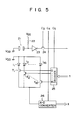
- a switch operation section 21 comprises the transparent electrode 4 and the lower cover 7 as the counter electrode.
- One of the electrodes is set at a high potential VDD (i.e. logic "1"), and the remaining electrode is connected to a low potential VSS (i.e. logic "0") through a resistor 22.
- the remaining electrode is also connected to the input terminal of a CMOS inverter 23.
- the input terminal of the inverter 23 is set at VSS, so that an output therefrom is set at logic "1".
- the optical input device is arranged in the following manner.
- the input terminals of the photosensors In are commonly connected to the high potential VDD, and the output terminals thereof are commonly connected through corresponding transfer gates Tn (1 ⁇ n 16).
- the gates Tn are operated in accordance with an output from a decoder 25.
- the decoder 25 decodes the output data n from the section 13 and time-divisionally generates pulses "0" to "15" which are supplied to the electrodes of the corresponding gates Tn. Therefore, the outputs from the photosensors In are supplied to an A/D (analog/digital) converter 26 through the corresponding transfer gates Tn.
- the A/D converter 26 converts an analog current to digital data, and an output from the A/D converter 26 is supplied as digital data x to the section 13.
- the decoder 25 and the A/D converter 26 are operated in response to the signals C4 and C5.
- step S1 the section 13 adds predetermined unit time data to timepiece data read out from the RAM 12 to obtain the current time which is then transferred to the RAM 12.
- step S2 an operation state of the key Sm is detected (step S2).
- the key Sm selects either the timepiece mode or the calculator mode.
- the section 11 discriminates the content of the mode register Fm of the RAM 12 (step S3).
- the content of the register Fm is updated (steps S4 and S5).
- data "0" in the register Fm represents the timepiece mode
- data "1" represents the calculator mode.
- step S6 the flow advances to step S8 and the section 11 checks whether or not the key AC is operated. If YES in step S8, all clear processing (step S9) is executed and then display processing (step S10) is executed. The electronic wristwatch is then set in the HALT mode. However, if NO in step S8, the signal C3 is supplied to the gate 24 to check whether or not a touch input is made (step S11). In this case, when the user wears the wristwatch and touches the electrode 4 on the upper surface of the glass plate 3 with a finger, an input signal to the inverter 23 is set at logic "1". The output from the inverter 23 is set at logic "0".
- the section 11 detects the presence/absence of the touch input in accordance with the output from the inverter 23. If NO in step S11, the flow advances to step S12, and a touch input flag is set at logic "0" in a flag register FT. Thereafter, step S10 is executed and the electronic wristwatch is set in the HALT mode. If YES in step S11, the content of the flag register FT is detected in step S13 to determine whether or not the logic level is "0". Since the content is set first at logic "0", the flag of logic "1 " is set in the register FT in step S14, and then key input processing (step S15) is executed to fetch the input data corresponding to the operated key.
- step S16 the section 11 determines the type of operated key. If the operated key is a ten key, register processing (step S17) is performed. However, when the operated key is any other key, operation processing (step S18) is performed. Thereafter, the registered or calculated data is displayed in the next step S10.
- step S13 key input processing is not performed, and the display content will not be updated.
- step S11 and S12 The user must release his finger from the electrode 4 and check the display content of the section 2B. Thereafter, the user must touch a portion corresponding to the desired key.
- Fig. 7 is a flow chart for explaining the detailed operation of key input processing of step S15.
- initialization is performed in step S21.
- Maximum intensity data a is transferred to the M register in the RAM 12.
- Numeric data "0" is transferred to the n register.
- the maximum intensity data a represents the case wherein no shadow is formed on the upper surface of the wristwatch and no light which could become incident on the photosensors In is shielded.
- the numeric data "0" transferred to the n register is an initial value for time-divisionally accessing the photosensors In.
- step S22 the numeric data in the n register is supplied to the section 14.
- the decoder 25 in the section 14 decodes the input numeric data and generates a signal of logic "0". For this reason, the gate T1 is turned on to transfer the output of the first photosensor 11 to the A/D converter 26.
- the intensity x of light incident on the photosensor 11 is generated from the section 14.
- the intensity data x is written in the X register in the RAM 12 in step S23.
- the content of the X register is compared with that of the M register to check in step S24 whether or not the content of the X register is smaller than that of the M register.
- the intensity of light received by the photosensor In is normally equal to the maximum light intensity a. However, when a finger is in contact with the electrode 4, a shadow is formed in the ambient region.
- step S24 When the operation in step S24 is performed to determine that a shadow is formed on the first photosensor 11, its output is smaller than the maximum intensity data a. However, if no shadow is formed on the first photosensor 11, the flow advances from step S24 to step S26 to check whether or not the content of the n register is "15". Since the content of the n register is set to be "0", the content of the n register is incremented by one (step S27), and the flow returns to step S22. For this reason, the numeric data supplied to the section 14 is set to be "1". The intensity data x of the second photosensor 12 is generated from the section 14.
- step S25 When discrimination is made that a shadow is formed on the photosensor 12 and the content of the X register is smaller than that of the M register in step S24, the flow advances to step S25. In this case, the content of the X register is transferred to the M register. At the same time, the content of the n register is transferred to the m register.
- the M register stores the intensity data of the photosensor 12 instead of the maximum intensity data a.
- the m register stores sensor number data "1" of the photosensor 12. Since the content of the n register is set at "1", the flow advances from step S26 to step S27, and the content of the n register is incremented by one to "2".
- the M register stores the minimum intensity data of the data generated from the 16 photosensors.
- the m register stores the sensor number data corresponding to the minimum intensity data. Even if a shadow is formed on a plurality of photosensors, the density of the shadow varies in accordance with the positions of the photosensors. The photosensor having the minimum intensity data is detected, and the key corresponding to the detected photosensor is regarded to have been operated. As a result, a plurality of keys will not be simultaneously turned on.
- the small square photosensor In having a side of 0.2 mm 2 or less can be obtained. Even if the photosensors In are formed above the liquid crystal display device 2, these photosensors will not interfere with readability of display contents. In this sense, the photosensors can be stacked on the device 2, and the function display of the photosensors In, that is, the function display of the keys can be easily performed. In addition, the input operation can be stably performed with high precision at low cost.
- the photosensors are used as an input means in correspondence with the respective keys of the calculator.
- the photosensors serve as an input means for a manual character recognition device.
- the present invention is applied to an electronic wristwatch with a character recognition device wherein when a user manually writes any character on the protection glass plate, the written character is recognized as input data.
- the application mode of the photosensors of the second embodiment is entirely different from that of the first embodiment.
- Other arrangements of the second embodiment, however, are substantially the same as those of the first embodiment.
- the same reference numerals in the second embodiment denote the same parts as in the first embodiment, and a detailed description thereof will be omitted.
- 36 photosensors In (1 ⁇ n ⁇ 36) are formed in a matrix form at positions corresponding to 36 (6 x 6) points along the X- and Y-axes on the lower surface of a protection glass plate 3.
- the coordinates of the respective photosensors are expressed by (1,1) to (6,6).
- a transparent electrode 4 (omitted in Fig. 8) constituting the touch switch device in the same manner as in the first embodiment is formed on the upper surface of the glass plate 3.
- the transparent electrode has a size corresponding to the entire region of the photosensors In.
- Fig. 9 shows a coordinate memory in a RAM 12.
- the memory stores a maximum of 20 coordinate data of each of the first, second and third strokes of each character.
- the column direction of the memory corresponds to the stroke number Z and the row direction of the memory corresponds to the coordinate number K.
- Fig. 10 is a flow chart for explaining the overall operation of the electronic wristwatch.
- step S31 initialization is performed to clear all registers K, Z, Fa, Fb and Fc.
- step S32 the character pattern manual input, i.e., the presence/absence of a touch input with respect to the electrode 4 is checked. If NO in step S32, the Fa register is detected in step S43 to check whether or not the content thereof is set to be "1". Since the content of the Fa register is initially set to be "0", the flow returns to step S32, and the operations up to the detection of the touch input are repeated.
- step S32 When a touch input is detected, data of "1 " is set in the Fa register in step S32.
- the data of logic “1 " is set in the Fa register at the beginning of the manual character pattern.
- the Fb register is checked in step S34 to check whether or not its content is set at logic "0". Since the content of the Fb register is initially set at logic "0", the flow advances to step S35.
- the content of the Z register is incremented by one.
- the Z register stores the column address, i.e., the stroke number in the coordinate memory of Fig. 9.
- step S36 data of logic "1 " is set in the Fb register, and data of logic "0" is set in the Fc register. Thereafter, key input processing in step S37 is executed.
- step S38 the number n of the currently detected photosensor having the minimum intensity level is compared with the number n' of the immediately preceding photosensor having the minimum intensity level. In this case, the photosensor having the minimum intensity level is updated in accordance with finger movement during manual input of the character pattern.
- the flow returns to step S32.
- the number n is not equal to the number n', the user has moved his finger.
- the flow advances to step S39.
- the sensor number n of the currently detected photosensor is updated as the number n' of the immediately preceding photosensor. Thereafter, the content of the K register is incremented by one in step S40.
- the K register stores the row addresses of the coordinate memory of Fig. 9.
- the currently detected sensor number n is translated to the corresponding coordinate data.
- the obtained coordinate data is stored at predetermined address areas Mz and k of the coordinate memory of Fig. 9 in step S42.
- the address areas Mz and k are accessed in accordance with the contents of the Z and K registers, respectively.
- the contents of the Z and K registers are set at logic "1", respectively.
- the coordinate memory is addressed in accordance with the contents of the Z and K registers.
- the currently detected coordinate data is stored as the first coordinates of the first stroke. In this manner, when the coordinate data is written, the flow returns to step S32, and the same operation as described above is repeated.
- the respective coordinate data of the first stroke are sequentially stored in the first stroke memory area of the coordinate memory.
- step S32 When the user finishes writing the first stroke of the character pattern and releases his finger from the electrode 4 so as to write the second stroke or upon input completion of a one-stroke character, this release is detected in step S32, and the flow advances to step S43. Since the content of the Fa register is set at "1", the flow advances to step S44 wherein the content of the Fb register is cleared. Data of "0" is set in the Fb register when the first stroke is written. The Fc register is checked in step S45 to determine whether or not its content is set at "0". Since the content of the Fc register is initially set at "0", the flow advances to step S46. In step S46, data of "1 " is set in the Fc register. Thereafter, the timer is cleared and started in step S47.
- This timer counts a predetermined period of time after one character is written and before the next character is started. When the timer does not count the predetermined period of time, such an operation is detected in step S48, and the flow returns to step S31. In this case, since data of "1 " is set in the Fc register, timer start operation is not performed, and the timer continues the counting operation.
- step S33 to S42 are sequentially performed again.
- the coordinate data for the second stroke are sequentially stored in the second stroke memory area of the coordinate memory.
- the same operation as described above is performed.
- the coordinate data for the third stroke are sequentially written in the third stroke memory area of the coordinate memory.
- step S48 the time-up is detected in step S48, and the flow advances to step S49.
- step S49 the coordinate data of the one character stored in the coordinate memory are compared with the data of the standard character pattern, and the similar standard character pattern is regarded as the input character data, thereby completing character recognition processing.
- the photosensors can be used as an input means.
- a photosensor In having the minimum light intensity is detected among the photosensors 11 to 116 and the key corresponding to the detected photosensor In is detected to have been operated.
- the photosensors are subjected to influences from shadows of fingers or a hand in accordance with an incident direction of external light, so that the photosensor having the minimum light intensity often does not coincide with the contact position. Correction is performed in consideration of the incident direction of the external light, as will be described in a third embodiment below.
- the arrangement of the third embodiment is the same as that shown in Figs. 1 to 5 of the first embodiment, and a detailed description thereof will be omitted.
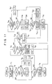
- step T1 time count processing is performed.
- An operation section 13 adds predetermined unit time data to time data read out from a RAM 12. The calculated current time data is supplied to the RAM 12.
- step T2 an operation state of a mode changing key Sm is detected in step T2.
- the key Sm selects either the timepiece mode or the calculator mode.
- step T3 the content of a mode register Fm in the RAM 12 is detected in step T3.
- the content of the mode register Fm is updated in steps T4 and T5.
- step T6 When the timepiece mode is detected in step T7 to be set, the current time calculated in the time count processing is supplied to a display section 17 in step T8. The current time is displayed on a digital display section 2A of a liquid crystal display device 2, and the electronic wristwatch is set in the HALT mode.
- step T7 when it is determined in step T7 that the calculator mode is set, the flow advances to step T9.
- the Fd register is checked in step T9 to determine whether or not its content is set at "1". Since the content of the Fd register is set at "1 upon switching the mode from the timepiece mode to the calculator mode, the flow advances to step T10 so as to determine whether or not touch input is present or absent. If NO in step T10, the electronic wristwatch is set in the HALT mode. However, if YES in step T10, the photo direction calculation processing is performed in step T11. When the photo direction of the external light is detected and the Fd register is reset, the electronic wristwatch is set in the HALT mode.
- step T13 it is checked whether or not an all clear key AC is operated.
- step T14 all clear processing
- step T15 display processing
- step T16 the electronic wristwatch is set in the HALT mode.
- a control signal C3 is supplied to a transfer gate 24 to check in step T16 whether or not a touch input is present.
- step T16 the flow advances to step T17, and a flag representing a touch input absent state is set to be "0" in a flag register FT. Thereafter, display processing in step T15 is performed and the electronic wristwatch is set in the HALT mode. However, if YES in step T16, the FT register is checked in step T18 whether or not its content is set to be "0". Since the content of the FT register is initially set to be "0”, a flag of logic "1 " is set in the FT register in step T19, and input data corresponding to the operated key is fetched.
- step T21 the type of key is discriminated.
- register processing is performed in step T22.
- calculation processing is performed in step T23. Thereafter, the registered or calculated result is displayed in step T15.
- the operated key is detected in accordance with the outputs from the photosensors In, and the proper operation is performed.
- the content of the FT register is kept at "1 " while the user is touching the electrode 4.
- the flow advances from step T18 to step T15, and key input processing is not performed. In this case, the display content will not be updated.
- the content of the FT register is reset to "0" in steps T16 and T17.
- the user wishes to enter another key input, he must release his finger from the electrode 4 and check the display content of the section 2B. Thereafter, a portion corresponding to the desired key must be touched.
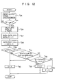
- Fig. 12 is a flow chart for explaining photo direction calculation processing of step T11
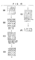
- Fig. 13 is a representation for explaining this operation.
- step T24 When the user touches the No. 9 key, the light intensities of the 16 photosensors are detected in step T24.
- the flow advances to step T25 to check whether or not N (e.g. 10) detection cycles are repeated. If NO in step T25, the flow returns to step T24 wherein the light intensities of the 16 photosensors are detected. If YES in step T25, the flow advances to step T26.
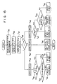
- Fig. 15 is a flow chart for explaining the detailed operation of key input processing of step T20 of Fig. 11.
- step T44 the 16 data are scanned (step T44) from the top from the left direction to the right direction in an order of E, F, G and H, as shown in Fig. 17.
- Ik ⁇ 0 the corresponding (k) key is selected in step T45.
- step T46 the 16 data are scanned from the top from the right direction to the right direction in an order of E, F, G and H as shown in Fig. 17. If Ik ⁇ 0 is established, the number of data satisfying Ik ⁇ 0 is counted in units of rows, and the flow advances to step T47 to check whether or not the count is "1". If YES in step T47, the (k) key corresponding to Ik ⁇ 0 is selected. However, if NO in step T47, the flow advances to step T48 to check whether or not (initial lk) > lk+4 is established. If YES in step T48, the flow advances to step T49 to select the (k + 4) key. However, if NO in step T48, the flow advances to step T50 to select the (k) key.
- the photosensors In are arranged on the lower surface of the glass plate 3.
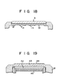
- the present invention is not limited to this arrangement, and can be constituted by that shown in Fig. 18.
- a transparent plate 31 of a synthetic resin or the like is disposed below a protection glass plate 3 to be spaced apart therefrom.
- a plurality of photosensors In are formed on the lower surface of the transparent plate 31. In this manner, the mounting position of the photosensors is not limited to the glass plate.
- the photosensors can be formed on an upper glass substrate of the liquid crystal display device.
- FIG. 19 is a sectional view showing the main part of the electronic wristwatch according to the fourth embodiment.
- a transparent protection glass plate 43 is pressed and fitted in an opening of the upper surface of a wristwatch case 41 to cover a liquid crystal display device 42.
- a transparent electrode 44 constituting a touch switch is formed on the upper surface of the glass plate 43.
- the electrode 44 has substantially the same size as that of the device 42.
- the electrode 44 detects the contact, thereby performing a switching operation.
- the case 41 is used as one electrode.
- a single photosensor 45 having substantially the same size as the display screen area is formed below the device 42.
- the photosensor 45 constitutes an optical input device which comprises monocrystalline silicon phototransistors, amorphous silicon phototransistors or amorphous photoconductive cells. An output from the photosensor is converted to a change in voltage, current or resistance in accordance with a change in light intensity.
- the photosensor 45 comprises amorphous silicon.
- the photosensor 45 is electrically connected to a printed circuit board having an LSI (large scale integrated circuit) thereon.
- the device 42 comprises a transmission type liquid crystal display device which is arranged on the front surface of the photosensor 45 to guide external light from the glass plate 43 to the photosensor 45.
- the device 42 is of a DSM (dynamic scattering mode) type wherein a high transmittance is obtained when no electrical field or a weak electrical field is applied thereto to efficiently transmit external light onto the upper surface side of the photosensor 45.
- DSM dynamic scattering mode
- this device 45 when an electrical field has a predetermined level or a high level, the liquid crystal molecules are held in a dynamic scattering state, so that the device 45 is kept opaque. In this state, external light is shielded so as to prevent light from becoming incident on the upper surface of the photosensor 45.
- the device 42 has an electrode structure driven by a dot matrix display system.
- 28 column electrodes 2A1 to 2A28 are arranged along the vertical direction, and 28 row electrodes 2B1 to 2B28 are arranged along the horizontal direction to constitute a 28 x 28 dot matrix display screen.
- the device 42 serves as a data display section for displaying a numeric value, a letter or the like by matrix-driving 28 x 28 dot pixels.
- the device 42 also serves as an optical input device together with the photosensor 45 arranged below the device 42.
- the device 42 of 28 x 28 dots is operated as a 7 x 7 dot matrix when one pixel comprises 4 x 4 dots or as a 14 x 14 dot matrix when one pixel comprises 2 x 2 dots.
- the circuit arrangement of the electronic wristwatch according to this embodiment will be described with reference to Figs. 21, 22 and 23.
- the electronic wristwatch is driven by a microprogram control system.
- a control section 51 constituted by a ROM (read-only memory) stores a microprogram for controlling the overall operation of the electronic wristwatch.
- the section 51 generates parallel microinstructions AD, DA, OP and NA (to be described below).
- the microinstruction AD is supplied as address data to a RAM (random access memory) 52.
- the microinstruction DA is supplied as numerical data to an operation section 53.
- the microinstruction OP is supplied as data to an operation decoder 55.
- the decoder 55 decodes the microinstruction OP to generate various control signals a, b, c, d1 to d5, gx and gy.
- the microinstruction NA is supplied to an address section 56.
- the section 56 supplies next address data to the section 51 so as to cause the section 51 to generate the microinstructions required for the next operation.
- the RAM 52 comprises an input register, an operation register and the like to perform time count processing, key input processing, operation processing and the like.
- the RAM 52 performs data read/write access in response to the control signal d1 from the decoder 55.
- the section 53 performs time count processing, key input processing, operation processing and the like in response to the control signal d2.
- the processing results are supplied to the RAM 52 and stored at the accessed address. At the same time, the processing results are also supplied to a display section 57 and a switch input section 54.
- the section 54 comprises a mode changing switch Sm for cyclically selecting the time count mode, the calculator mode and the data bank mode, a read/write changing switch S R/W for selecting the read/write mode in the data bank mode and a page change switch SP for changing the page in the data bank mode. These switches are push-button switches arranged at two side surfaces of the wristwatch.
- the section 54 generates a key code corresponding to the depressed switch in accordance with the signal d3.
- the key code is supplied to the section 53.
- the section 53 receives a touch input signal t generated from a touch switch section 58 in response to the signal d4.
- the section 53 also receives detection data x representing the light intensity and generated from the photosensor 19 in response to the signal d5.
- the display section 57 has the device 42 and a display driver and is controlled in response to the signals a, b, c, gx and gy.
- the section 53 performs discrimination operation, it generates a signal e representing the presence/absence of data and a signal f representing the presence/absence of a carry to the section 56, thereby performing address conversion.
- a reference clock signal from an oscillator 60 is divided by a frequency divider 61, and a frequency-divided 16-Hz signal is supplied to the section 56. Time count processing can be performed for every 1/16 second in response to the 16-Hz signal.
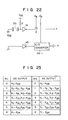
- a touch switch TS comprises the electrode 44 as one electrode, and the lower cover (the wristwatch case 41) as the other electrode, as described above.
- the electrode 44 is kept at a high potential VDD (i.e. logic "1 "), and the lower cover is grounded at a low voltage VSS (i.e. logic "0") through a resistor R.
- the lower cover is also connected to the input terminal of a CMOS inverter IN.
- the input terminal of the inverter IN is set at the low potential VSS, and an output therefrom is set at logic "1 ". However, when the electrodes are electrically connected through the user's body, the output from the inverter IN is set at logic "0".
- the output from the inverter IN is supplied as an input signal through a transfer gate G. An output from the gate G is normally kept at a high impedance. The gate G is enabled only when the signal d4 is supplied to the control gate thereof. In the photosensor section 59, the input terminal of the photosensor 45 is connected to the high potential VDD.
- An output from the photosensor 45 is supplied to an A/D (analog/digital) converter 59-1.
- the A/D converter 59-1 converts a current from the photosensor 45 to a digital signal.
- the digital signal from the A/D converter 59-1 is supplied as digital data x.
- the A/D converter 59-1 is controlled in response to the signal d5.
- Fig. 20 shows the arrangement of the display section 57.
- the electrodes 2A1 to 2A28 of the device 42 are connected to output terminals X1 to X28 of each of decoder drivers Xa and Xb, respectively.
- the electrodes 2B1 to 2B28 are connected to the output terminals Y1 to Y28 of each of decoder drivers Ya and Yb, respectively.
- the drivers Xa and Ya receive the signal a
- the drivers Xb and Yb receive the signal b.
- the signal a is generated when character input processing is performed in the calculator mode so as to drive the drivers Xa and Ya.
- the signal b is generated in character input processing of the write mode of the data bank mode to drive the drivers Xb and Yb.
- the drivers Xa and Xb receive data m1 from the section 53 through gates G1 and G2 which are enabled in response to the signal gx.
- the drivers Ya and Yb receive data m2 from the section 53 through gates G3 and G4 which are enabled in response to the signal gy.
- the data m1 and m2 supplied to the drivers Xa and Ya operated in the calculator mode comprise numerical data varying from 0 to 6.
- the drivers Xa and Ya decode the numerical data to sequentially generate parallel 4- bit nondrive signals and remaining signals as drive signals.
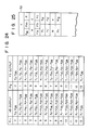
- Fig. 23 is a table showing the terminals at which drive signals from the drivers Xa and Ya appear.
- the nondrive signals appear at the terminals X1 to X4, and the drive signals appear at the remaining terminals X5 to X28.
- the nondrive signals appear at the terminals Y1 to Y4 and the drive signals appear at the remaining terminals Y5 to Y28.
- the device 42 is driven in the calculator mode, as shown in Fig. 23.
- the pixels, each having 4 x 4 dots, are time-divisionally driven in the 7 x 7 matrix.
- the data m1 and m2 consist of numeric values varying from 0 to 13 are supplied to the drivers Xb and Yb and decoded by the drivers Xb and Yb operating in the write mode of the data bank mode.
- the drivers Xb and Yb sequentially generate parallel 2-bit nondrive signals and the remaining signals as drive signals.
- Fig. 24 shows terminals at which drive signals from the drivers Xb and Yb appear. For example, when the data m1 is set at logic "0", the nondrive signals appear at the terminals X1 and X2 and drive signals appear at the remaining terminals X3 to X28.
- the device 2 of 28 x 28 dots is operated as a device of 7 x 7 matrix (i.e. operated with low resolution) in the calculator mode in response to outputs from the drivers Xa and Ya.
- the device 2 is operated as a device of 14 x 14 matrix (i.e. operated with high resolution) in the write mode of the data bank mode in response to outputs from the drivers Xb and Yb.
- Each pixel is time-divisionally held in the nondrive state while the remaining pixels are driven, thereby causing the nondriven pixels to transmit light and driven pixels to shield light.
- the display data from the section 53 is converted by a display driver 57-1 to a display drive signal which is then supplied to the device 42.
- the driver 57-1 is driven in response to the signal c.
- the signal c is generated while the signals a and b are being generated, thereby setting the section 42 as a data display section.
- Fig. 25 shows part of an arrangement of the RAM 52.
- the RAM 52 has a data bank memory or the like in addition to the registers for data entry, display and calculation.
- the T register is a time count register for storing the current time data.
- the FM register is a mode register for storing a mode flag for selecting one of the time count mode, the calculator mode and the data bank mode by the switch Sm.
- the Fm register is a mode register for storing a mode flag set/reset by the switch S R/W in the data bank mode.
- the P register is a page register for storing a page number of the data bank memory.
- the A register is a register for storing data for determining whether the device 42 is operated with low or high resolution.
- the Z register is a stroke counter for counting a stroke number of a character manually written at the optical input device.
- the RAM 52 also has the Fa, Fb and Fc registers, the n1 and n2 registers, the n1' and n2' registers, the M and x registers and the m1 and m2 registers so as to perform character input processing and coordinate input processing which will be described later.
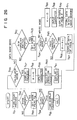
- step S51 Time count processing is executed in step S51 wherein the section 53 adds predetermined unit time data to the time count data read out from the T register in the RAM 52 to calculate the current time which is then transferred as the updated time count data to the T register in the RAM 52.
- step S52 the operating state of the switch Sm (step S52). If YES in step S52, the mode flag in the FM register in the RAM 52 is updated in accordance with the operating state of the switch Sm (step S53).
- step S54 the updating of the content in the FM register is detected in step S54.
- the time count data obtained by the time count processing is displayed in step S55, and the electronic wristwatch is set in the HALT mode.
- step S55 the signal c is supplied to the section 57 to drive the driver 57-1.
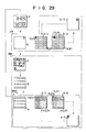
- the device 42 is driven as a device of 28 x 28 dot matrix in response to the output from the driver 57-1 to display date (9.05) and the current time (12:30) in the digital form, as indicated by a in Fig. 29.
- step S54 determines in step S54 that the current mode is a mode excluding the time count mode
- the flow advances to step S56, and the section 53 checks whether or not the calculator mode is set. If YES in step S56, display processing (step S57) is started. When no data is entered in the initial state immediately after the calculator mode is set, number "0" is displayed (b in Fig. 29).
- CR in Fig. 29 represents the driven state of the device 42 in the calculator mode.
- the device 42 serves as the optical input device together with the photosensor 45, the device 42 has a 7 x 7 matrix. In this case, numeric data "6" is set in the A register (step S58).
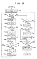
- step S59 the character pattern manually written on the glass plate 3 is optically detected to obtain an input character, thus performing character input processing (flow in Fig. 27).
- step S60 when the input data represents a numeric value, register processing is performed. When the input data represents a function symbol, calculation processing is performed. Display processing (step S61) of the registered or calculated data is performed. In display processing (step S61), when the drivers Xa and Ya in the section 57 are being operated in response to the signal b, the drivers Xa and Ya are stopped in response to the signal a.
- step S61 the signal c is supplied to the driver 57-1 which is driven to receive registered or calculated data to display it.
- the electronic wristwatch is held in the HALT mode.
- step S62 the flow advances to step S62 to check the operating state of the switch Sp /w . If YES in step S62, the mode flag in the Fm register is updated (step S63). When the read mode is set, this mode is detected in step S64, and the flow advances to step S65 to check the operating state of the switch SP. If YES in step S65, the content of the P register is incremented by one to obtain the next page (step S66). The one-page data stored at the address accessed by the content of the P register is read out from the data bank memory in the RAM 52 and is supplied to the section 17 which then displays the one-page data, as shown in c of Fig. 29.
- Names and telephone numbers which are stored as the one-page data in the data bank memory are displayed.
- the content of the P register is incremented by one every time the switch SP is operated, so that the contents of the data bank memory can be sequentially read out and displayed in units of one-page data.
- DB in Fig. 29 shows the driven state of the device 42 in the data bank mode.
- the switch SP is operated in the read mode to display data of a specific page if the user wishes to update the data of the specific page. However, when the user wishes to add new data, an empty page is displayed. For example, when the user wishes to add new data, he operates the switch SP until an empty page shown in d of Fig. 29 appears. When the empty page is displayed, the user operates the switch S R/w . In step S62, the section 53 detects that the switch S R/W is operated. In step S63, the mode flag in the Fm register is updated. The section 53 then detects in step S64 that the write mode is set, so that the operations in steps S68 to S70 are performed. DBW in Fig.
- step S68 shows the driven state of the device 42 in the data bank write mode.
- the device 42 In the data bank write mode, the device 42 is driven as a device of 14 x 14 matrix.
- step S68 numerical data "13" is stored in the A register.
- Possible input data in the data bank mode comprise numbers 0 to 9 and letters A to Z.
- step S69 input processing of the manually written character pattern is performed in the same manner as in step S59. The entered character is displayed in step S70.
- step S70 when the drivers Xb and Yb in the section 57 are being operated in response to the signal b, the signal b is stopped to stop the drivers Xb and Yb. Thereafter, the signal c is supplied to the driver 57-1 which receives the input character so as to display it. Subsequently, the input character is stored in the data bank memory (step S71), and the electronic wristwatch is set in the HALT mode. In the data bank write mode, the manually entered characters are sequentially stored in the data bank memory.
- step S81 initialization is performed in step S81. More particularly, the contents of the Z, Fa, Fb and Fc registers are cleared.
- the section 53 then checks in step S82 whether or not a touch input to the electrode 44 is entered. In this case, when the user wears a wristwatch and touches the electrode 44 on the glass plate 43, the input signal to the inverter IN in the section 58 is set at logic "1", and an output signal from the inverter IN is set at logic "0".
- the section 53 detects the presence/absence of the touch input in accordance with the output from the inverter IN. If NO in step S82, the flow advances to step S93.
- the section 53 checks in step S93 whether or not the content of the Fa register is set to be "1". Since the initial content of the Fa register is set to be "0”, the flow returns to step S82, and the electronic wristwatch is set in the HALT mode wherein the above operations are repeated until a touch input is detected.
- step S83 the signal c is no longer supplied to the driver 57-1 and the content displayed on the device 42 is deleted.
- the display content is deleted so as to cause the device 42 to serve as the optical input device.
- the same deletion as described above is also performed in the data bank mode; the display content of the empty page in e of Fig. 29 is deleted.
- step S84 when the touch input is detected, "1" is set in the Fa register (step S84). Therefore, "1 " is set in the Fa register at the beginning of character pattern writing.
- the section 53 checks in step S85 whether or not the content of the Fb register is set to be "0".
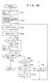
- step S86 Since the initial content of the Fb register is set to be "0", the flow advances to step S86 to increment the count of the Z register for storing the stroke number of the manually written character pattern. Since the first stroke of the character is first entered, the content of the Z register is set to be "1". In step S87, "1 is set in the Fb and Fc registers. Thereafter, coordinate input processing (step S88) is started. This coordinate input processing is performed in accordance with a flow chart of Fig. 28.
- step S101 Initialization is performed in step S101. More particularly, an initial value a is set in the M register in the RAM 52, and the m1 and m2 registers are cleared.
- step S102 when the calculator mode is set, the signal a is generated to designate the drivers Xa and Ya in the section 57.
- the signal b is generated to designate the drivers Xb and Yb.
- step S103 the contents of the m1 and m2 registers are generated in synchronism with the signals gx and gy and supplied to the section 57.
- the calculator mode is exemplified.
- the signal a is supplied to the section 57, so that the drivers Xa and Ya are rendered operative and the drivers Xb and Yb are rendered inoperative.
- the data m1 and m2 are supplied to the drivers Xa and Ya which generate outputs shown in Fig. 23, respectively.
- the device 42 is operated as a device of 7 x 7 matrix since each pixel comprises 4 x 4 dots. Since both the data m1 and m2 are set at logic "0", nondrive signals appear at the terminals X1, X2, X3 and X4 of the driver Xa, and drive signals appear at the terminals X5 to X28 thereof.
- Nondrive signals appear at the terminals Y1, Y2, Y3 and Y4 of the driver Ya, and drive signals appear at terminals Y5 to Y28 thereof.
- the point (0,0) is held in the nondrive state and the remaining points are set in the drive state at the beginning. In this state, only the pixel at point (0,0) is held in the shutter ON state so as to transmit light, and the remaining pixels are held opaque to shield light. For this reason, in the photosensor section 59, light incident on the pixel at point (0,0) is detected by the photosensor 45.
- An output signal from the photosensor 45 is converted by an A/D converter 59-1 to the digital data x.
- the digital data x from the photosensor 45 is stored in the X register in the RAM 52 in step S104.
- the section 53 compares the content of the X register with that of the M register to check in step S105 whether or not the content of the X register is smaller than that of the M register.
- no shadow is formed on the upper surface of the wristwatch, so that the M register stores the maximum intensity a obtained from the pixel of 4 x 4 dots of the device 42 while the external light is not shielded at all.
- a shadow is formed at adjacent portions around a portion which contacts the finger.
- the density of the shadow in the adjacent portions varies, so that the intensities of light incident on the photosensor 59 corresponding to the adjacent portions vary.
- the light intensity is lower than the maximum intensity a.
- the flow advances from step S105 to step S107.
- the section 53 checks whether or not the values of the m1 and m2 registers are equal to the preset value of the A register.
- step S108 In the calculator mode, since "b" is set in the A register and "0" is set in the m1 and m2 registers, the flow advances to step S108.
- the section 53 checks again in step S108 whether or not the value of the m1 register is the same as that of the A register. Even in this case, the value of the m1 register is set to be "0" and is not the same as that of the A register.
- the flow advances to step S111 to increment the value of the m1 register, and the flow returns to step S103. In this case, the contents of the m1 and m2 registers are set to be "1 and "0", respectively.
- step S105 the content of the X register is transferred to the M register.
- step S106 the contents of the m1 and m2 registers are transferred to the n1 and n2 registers, respectively.
- the currently detected intensity is stored in the M register in place of the maximum intensity.
- step S111 the value of the m1 register is incremented by one to obtain "2". This operation is repeated until the value of the m1 register coincides with that of the A register. In the calculator mode, the above operation is repeated until the value of the m1 register reaches "6".
- the data (m1,m2) i.e. (0,0), (1,0),... (6,0)) are supplied to the section 57, so that six pixels in the first line of the device 2 are selectively set in the shutter ON state.
- step S108 When the value of the m1 register reaches "6", the content of "6" is detected in step S108. The flow advances to step S109. In step S109, the value of the m2 register is incremented by one to "1". After the value of the m1 register is cleared in step S110, the flow advances to step S103. In this cycle, the value of the m1 register is incremented up to "6" while the value of the m2 register is set to be “1". The six pixels along the second line of the device 42 are thus selectively held in the shutter ON state. The above operations are repeated until both the values of the m1 and m2 registers reach "6". The minimum intensity of the intensities of the 49 (7 x 7) pixels is stored in the M register.
- the X- and Y-coordinate data corresponding to the minimum intensity are stored in the n1 and n2 registers, respectively. Even if shadows are formed on portions corresponding to a plurality of pixels, the portion contacting the finger has the minimum intensity. When the coordinates of the finger contacting portion are detected, the portion which actually contacts the finger can be detected.
- the same operation as described above can also be performed in the data bank write mode.
- the drivers Xb and Yb are held operative and "13" is preset in the A register.
- the device 42 serves as a device of 14 x 14 matrix in accordance with the outputs from the drivers Xb and Yb, as shown in Fig. 24.
- the above operation states are illustrated in e-1 and e-2 of Fig. 29.
- the pixels corresponding to points (0,0) to (13,13) are selectively held in the shutter ON state. While all the pixels are sequentially held in the shutter ON state, the coordinates of a pixel having the minimum intensity are detected.
- step S89 in the flow chart of Fig. 27 is executed.
- step S89 the currently detected coordinate data n1 and n2 are compared with the immediately preceding coordinate data n1' and n2'. In this case, while the user moves his finger to enter a character pattern, the position of the pixel having the minimum intensity is also moving.
- the flow returns to step S82.
- the flow advances to step S90.
- the immediately preceding data n1' and n2' are updated to the currently detected data n1 and n2, respectively.
- the currently detected data n1 and n2 are stored at a predetermined address of the coordinate memory in the RAM 52.
- the detected coordinates are stored as the first coordinate data of the first stroke.
- the flow returns to step S82.
- the above operation is repeated while the finger is in contact with the electrode 44.
- the respective coordinate data of the first stroke are sequentially stored in the coordinate memory.
- the content of the Fb register is set to be "1 " while the first stroke is entered, and thus the value of the Z register is not incremented (steps S85 and S86).
- step S82 When the user finishes writing the first stroke and releases his finger from the electrode 44 so as to start writing the second stroke or so as to complete writing of a one-stroke character, such a release is detected in step S82.
- the flow advances to step S93. Since the content of the Fa register is set to be “1 ", the flow advances to step S94 and the Fb register is cleared.
- the content of the Fb register is reset to "0".
- the section 53 checks in step S45 whether or not the content of the Fc register is set to be "0". Since the initial content of the Fc register is set to be "0", the flow advances to step S96. In step S96, "1 " is set in the Fc register, and the timer is cleared and started (step S97).
- the timer counts a time interval between the first character write time and the second character write time.
- the section 53 detects in step S98 that the predetermined period of time has not elapsed. Thereafter, the flow returns to step S82.
- the flow advances to S93 through S95. In this case, since "1 " is set in the Fc register, the timer will not be cleared or started, but continues counting.
- step S98 When the predetermined period of time has elapsed, the time-up operation is detected in step S98, and the flow advances to step S99.
- the coordinate data of one character which is stored in the coordinate memory is compared with the prestored data of the standard character pattern. The most similar pattern is selected as the input character data, thus completing character recognition processing.
- the section 53 determines that one-character data is stored.
- step S61 in the calculator mode or step S83 in the data bank write mode is performed.
- step S61 in the calculator mode or step S83 in the data bank write mode is performed.
- the input data is displayed as register data, as shown in b-3 of Fig. 29.
- letter "E” is entered in the data bank write mode, the letter is displayed, as shown in e-3 of Fig. 29.
- the data input enable state is restored, as shown in b-1 or e-1 of Fig. 29.
- the optical input device comprises the photosensor 45 and the liquid crystal display device 42 for normally displaying time or the like.
- the device 42 serves as an optical shutter. A stacking structure of the photosensor 45 and the device 42 can be obtained. As a result, an additional mounting space for the optical input device need not be provided on the upper surface of the wristwatch case.
- the optical input device of this embodiment optimally serves as an external input means for an electronic wristwatch or a compact electronic calculator.
- the electrode 4 is formed on the upper surface of the glass plate 43.
- a finger does not contact the electrode 44, no character input processing is performed even if a shadow is formed on the glass plate 43. Therefore, even if a shadow is formed on the glass plate or an intensity is rapidly changed, data input is not performed, thereby effectively preventing erroneous data input.
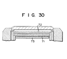
- the optical input device may have an arrangement as shown in Fig. 30.
- a TN (twisted nematic) type liquid crystal display device 72 is arranged above a DSM type liquid crystal display device 71.
- a photosensor 73 is arranged below the device 71.
- the entire surface of the device 72 is set opaque to obtain a white background to improve contrast when data such as time data is displayed on the device 72, thereby providing a clear display.
Landscapes
- Engineering & Computer Science (AREA)
- General Engineering & Computer Science (AREA)
- Theoretical Computer Science (AREA)
- Physics & Mathematics (AREA)
- General Physics & Mathematics (AREA)
- Human Computer Interaction (AREA)
- Electric Clocks (AREA)
- Input From Keyboards Or The Like (AREA)
Claims (14)
caractérisé en ce que
Applications Claiming Priority (4)
| Application Number | Priority Date | Filing Date | Title |
|---|---|---|---|
| JP59123793A JPS613233A (ja) | 1984-06-18 | 1984-06-18 | 光学的入力装置 |
| JP123793/84 | 1984-06-18 | ||
| JP14155084U JPS6160363U (fr) | 1984-09-20 | 1984-09-20 | |
| JP141550/84 | 1984-09-20 |
Publications (3)
| Publication Number | Publication Date |
|---|---|
| EP0165548A2 EP0165548A2 (fr) | 1985-12-27 |
| EP0165548A3 EP0165548A3 (en) | 1988-11-30 |
| EP0165548B1 true EP0165548B1 (fr) | 1992-03-18 |
Family
ID=26460620
Family Applications (1)
| Application Number | Title | Priority Date | Filing Date |
|---|---|---|---|
| EP85107239A Expired EP0165548B1 (fr) | 1984-06-18 | 1985-06-13 | Petit appareil électronique comportant un système d'entrée optique |
Country Status (3)
| Country | Link |
|---|---|
| US (1) | US4671671A (fr) |
| EP (1) | EP0165548B1 (fr) |
| DE (1) | DE3585641D1 (fr) |
Cited By (1)
| Publication number | Priority date | Publication date | Assignee | Title |
|---|---|---|---|---|
| US11567457B2 (en) | 2014-09-02 | 2023-01-31 | Apple Inc. | Wearable electronic device |
Families Citing this family (54)
| Publication number | Priority date | Publication date | Assignee | Title |
|---|---|---|---|---|
| US4764910A (en) * | 1985-03-08 | 1988-08-16 | Citizen Watch Co., Ltd. | Electronic timepiece |
| DE3622632C2 (de) * | 1986-07-05 | 1995-11-30 | Fichtel & Sachs Ag | Elektronisches Gerät zur Messung und Anzeige der Geschwindigkeit und weiterer Daten bei einem Fahrrad |
| US6311419B1 (en) | 1989-12-31 | 2001-11-06 | Smartlight Ltd. | Dedicated mammogram viewer |
| IL92936A (en) * | 1989-12-31 | 1998-02-08 | Smartlight Ltd | Self-masking transparency viewing apparatus |
| US5105186A (en) * | 1990-05-25 | 1992-04-14 | Hewlett-Packard Company | Lcd touch screen |
| WO1993001564A1 (fr) * | 1991-07-11 | 1993-01-21 | Dan Inbar | Dispositif d'affichage detectant des positions |
| US6088941A (en) * | 1992-04-06 | 2000-07-18 | A.D.P. Adaptive Visual Perception Ltd. | Transparency viewing apparatus |
| EP0918241A3 (fr) * | 1993-11-28 | 1999-06-23 | Smartlight Limited | Dispositif d'observation d'image transparente |
| CH686601B5 (fr) | 1994-08-02 | 1996-11-15 | Asulab Sa | Dispositif d'identification d'un caractère transcrit sur une surface et procédé d'identification d'un tel caractère, notamment pour une montre. |
| FR2745400B1 (fr) | 1996-02-23 | 1998-05-07 | Asulab Sa | Dispositif d'entree de donnees dans des moyens electroniques de traitement de ces donnees |
| US5963276A (en) * | 1997-01-09 | 1999-10-05 | Smartlight Ltd. | Back projection transparency viewer with overlapping pixels |
| JP4187809B2 (ja) * | 1997-09-08 | 2008-11-26 | シチズンホールディングス株式会社 | 小型電子機器 |
| US7009663B2 (en) | 2003-12-17 | 2006-03-07 | Planar Systems, Inc. | Integrated optical light sensitive active matrix liquid crystal display |
| US7408598B2 (en) | 2002-02-20 | 2008-08-05 | Planar Systems, Inc. | Light sensitive display with selected interval of light sensitive elements |
| US7053967B2 (en) * | 2002-05-23 | 2006-05-30 | Planar Systems, Inc. | Light sensitive display |
| US20080084374A1 (en) * | 2003-02-20 | 2008-04-10 | Planar Systems, Inc. | Light sensitive display |
| US7773139B2 (en) | 2004-04-16 | 2010-08-10 | Apple Inc. | Image sensor with photosensitive thin film transistors |
| US7607243B2 (en) | 2006-05-03 | 2009-10-27 | Nike, Inc. | Athletic or other performance sensing systems |
| JP5550077B2 (ja) | 2007-09-07 | 2014-07-16 | ナイキ インターナショナル リミテッド | 運動機能性を有する装着可能な装置アセンブリ |
| FI20085022A0 (fi) | 2008-01-11 | 2008-01-11 | Navigil Oy | Tietokonelaite |
| EP2700434A3 (fr) | 2008-04-02 | 2014-07-02 | Nike International Ltd. | Ensemble de dispositif portable ayant une fonctionnalité athlétique |
| JP2012163581A (ja) * | 2009-06-19 | 2012-08-30 | Sharp Corp | 表示装置 |
| US9310923B2 (en) | 2010-12-03 | 2016-04-12 | Apple Inc. | Input device for touch sensitive devices |
| US9329703B2 (en) | 2011-06-22 | 2016-05-03 | Apple Inc. | Intelligent stylus |
| US8928635B2 (en) | 2011-06-22 | 2015-01-06 | Apple Inc. | Active stylus |
| US8638320B2 (en) | 2011-06-22 | 2014-01-28 | Apple Inc. | Stylus orientation detection |
| US9176604B2 (en) | 2012-07-27 | 2015-11-03 | Apple Inc. | Stylus device |
| US9557845B2 (en) | 2012-07-27 | 2017-01-31 | Apple Inc. | Input device for and method of communication with capacitive devices through frequency variation |
| US9652090B2 (en) | 2012-07-27 | 2017-05-16 | Apple Inc. | Device for digital communication through capacitive coupling |
| US10048775B2 (en) | 2013-03-14 | 2018-08-14 | Apple Inc. | Stylus detection and demodulation |
| US9753436B2 (en) | 2013-06-11 | 2017-09-05 | Apple Inc. | Rotary input mechanism for an electronic device |
| US10845901B2 (en) | 2013-07-31 | 2020-11-24 | Apple Inc. | Touch controller architecture |
| KR20220116337A (ko) | 2013-08-09 | 2022-08-22 | 애플 인크. | 전자 디바이스용 촉각 스위치 |
| US10048802B2 (en) | 2014-02-12 | 2018-08-14 | Apple Inc. | Rejection of false turns of rotary inputs for electronic devices |
| US10067618B2 (en) | 2014-12-04 | 2018-09-04 | Apple Inc. | Coarse scan and targeted active mode scan for touch |
| EP3251139B1 (fr) | 2015-03-08 | 2021-04-28 | Apple Inc. | Joint d'étanchéité compressible pour mécanismes d'entrée à rotation et translation |
| US10551798B1 (en) | 2016-05-17 | 2020-02-04 | Apple Inc. | Rotatable crown for an electronic device |
| US10474277B2 (en) | 2016-05-31 | 2019-11-12 | Apple Inc. | Position-based stylus communication |
| US10061399B2 (en) | 2016-07-15 | 2018-08-28 | Apple Inc. | Capacitive gap sensor ring for an input device |
| US10019097B2 (en) | 2016-07-25 | 2018-07-10 | Apple Inc. | Force-detecting input structure |
| US10962935B1 (en) | 2017-07-18 | 2021-03-30 | Apple Inc. | Tri-axis force sensor |
| US11360440B2 (en) | 2018-06-25 | 2022-06-14 | Apple Inc. | Crown for an electronic watch |
| US11561515B2 (en) | 2018-08-02 | 2023-01-24 | Apple Inc. | Crown for an electronic watch |
| US12259690B2 (en) | 2018-08-24 | 2025-03-25 | Apple Inc. | Watch crown having a conductive surface |
| CN211293787U (zh) | 2018-08-24 | 2020-08-18 | 苹果公司 | 电子表 |
| CN209625187U (zh) | 2018-08-30 | 2019-11-12 | 苹果公司 | 电子手表和电子设备 |
| US11194299B1 (en) | 2019-02-12 | 2021-12-07 | Apple Inc. | Variable frictional feedback device for a digital crown of an electronic watch |
| US11550268B2 (en) | 2020-06-02 | 2023-01-10 | Apple Inc. | Switch module for electronic crown assembly |
| US12153764B1 (en) | 2020-09-25 | 2024-11-26 | Apple Inc. | Stylus with receive architecture for position determination |
| US12092996B2 (en) | 2021-07-16 | 2024-09-17 | Apple Inc. | Laser-based rotation sensor for a crown of an electronic watch |
| US12396686B2 (en) | 2021-08-31 | 2025-08-26 | Apple Inc. | Sensing health parameters in wearable devices |
| US12189347B2 (en) | 2022-06-14 | 2025-01-07 | Apple Inc. | Rotation sensor for a crown of an electronic watch |
| US12596334B2 (en) | 2023-02-07 | 2026-04-07 | Apple Inc. | Crown for an electronic watch |
| US12669784B2 (en) | 2023-03-24 | 2026-06-30 | Apple Inc. | Crown sensing system for an electronic watch |
Family Cites Families (6)
| Publication number | Priority date | Publication date | Assignee | Title |
|---|---|---|---|---|
| GB1494901A (en) * | 1974-04-30 | 1977-12-14 | Suisse Horlogerie | Data entry and decoding system |
| US4070649A (en) * | 1976-12-01 | 1978-01-24 | Said Sanford J. Wright, By Said Peter Anderson And Said Ralph Grimes | Multi-modal data input/output apparatus and method compatible with bio-engineering requirements |
| US4139837A (en) * | 1977-06-22 | 1979-02-13 | Creative Ventures, Inc. | Information entry system |
| JPS5685792A (en) * | 1979-12-14 | 1981-07-13 | Citizen Watch Co Ltd | Liquid crystal display unit |
| US4477797A (en) * | 1980-12-12 | 1984-10-16 | Citizen Watch Company Limited | Data input device for electronic device |
| US4468131A (en) * | 1982-05-03 | 1984-08-28 | Asulab S.A. | Electronic watch having a non-moving means of control |
-
1985
- 1985-06-10 US US06/743,381 patent/US4671671A/en not_active Expired - Lifetime
- 1985-06-13 DE DE8585107239T patent/DE3585641D1/de not_active Expired - Lifetime
- 1985-06-13 EP EP85107239A patent/EP0165548B1/fr not_active Expired
Cited By (1)
| Publication number | Priority date | Publication date | Assignee | Title |
|---|---|---|---|---|
| US11567457B2 (en) | 2014-09-02 | 2023-01-31 | Apple Inc. | Wearable electronic device |
Also Published As
| Publication number | Publication date |
|---|---|
| EP0165548A2 (fr) | 1985-12-27 |
| EP0165548A3 (en) | 1988-11-30 |
| DE3585641D1 (de) | 1992-04-23 |
| US4671671A (en) | 1987-06-09 |
Similar Documents
| Publication | Publication Date | Title |
|---|---|---|
| US4671671A (en) | Small electronic apparatus with optical input device | |
| CA1244162A (fr) | Segment de recouvrement sensible au toucher | |
| US4139837A (en) | Information entry system | |
| US5319386A (en) | Ideographic character selection method and apparatus | |
| US4224615A (en) | Method of using a liquid crystal display device as a data input device | |
| US4655552A (en) | Flat panel display device having on-screen data input function | |
| KR950001730B1 (ko) | 옵티컬 인텔리젠트 키보드 구조체 | |
| US4477797A (en) | Data input device for electronic device | |
| US7136048B2 (en) | Electrically erasable writing surface | |
| KR100298974B1 (ko) | 수기 데이터 입력 수단을 구비한 휴대용 단말 장치 | |
| US6028591A (en) | Keyboard with flexible display and prompt capability | |
| US5202844A (en) | Computer having integral type hand writing input/display device and keyboard | |
| US4276541A (en) | Display control of hand-written, memorized pattern at a preselected time | |
| US20060239746A1 (en) | Systems and methods for computer input | |
| US20010003539A1 (en) | Telephone keypad having a dual-switch button | |
| US4803463A (en) | Key input means with changeable display means for displaying key functions | |
| GB2139762A (en) | An input device and a method of inputting data to a computer system | |
| US20030169240A1 (en) | Character input apparatus and method | |
| US6229919B1 (en) | Character data input apparatus | |
| CN107479768B (zh) | 一种显示面板及显示装置 | |
| US4504829A (en) | Electronic equipment | |
| KR100469704B1 (ko) | 트랙볼을이용한휴대폰사용자인터페이스장치 | |
| JPH07120233B2 (ja) | 光学的入力装置付小型電子機器 | |
| KR100311892B1 (ko) | 소형기기 또는 데스크탑 전화기에서 숫자 또는 문자를 빠르게 입력하는 장치 | |
| CN212084103U (zh) | 一种多语种切换的多功能键盘 |
Legal Events
| Date | Code | Title | Description |
|---|---|---|---|
| PUAI | Public reference made under article 153(3) epc to a published international application that has entered the european phase |
Free format text: ORIGINAL CODE: 0009012 |
|
| AK | Designated contracting states |
Designated state(s): CH DE FR GB LI |
|
| PUAL | Search report despatched |
Free format text: ORIGINAL CODE: 0009013 |
|
| AK | Designated contracting states |
Kind code of ref document: A3 Designated state(s): CH DE FR GB LI |
|
| 17P | Request for examination filed |
Effective date: 19890526 |
|
| 17Q | First examination report despatched |
Effective date: 19900731 |
|
| GRAA | (expected) grant |
Free format text: ORIGINAL CODE: 0009210 |
|
| AK | Designated contracting states |
Kind code of ref document: B1 Designated state(s): CH DE FR GB LI |
|
| REF | Corresponds to: |
Ref document number: 3585641 Country of ref document: DE Date of ref document: 19920423 |
|
| ET | Fr: translation filed | ||
| PLBE | No opposition filed within time limit |
Free format text: ORIGINAL CODE: 0009261 |
|
| STAA | Information on the status of an ep patent application or granted ep patent |
Free format text: STATUS: NO OPPOSITION FILED WITHIN TIME LIMIT |
|
| 26N | No opposition filed | ||
| PGFP | Annual fee paid to national office [announced via postgrant information from national office to epo] |
Ref country code: GB Payment date: 19980604 Year of fee payment: 14 |
|
| PGFP | Annual fee paid to national office [announced via postgrant information from national office to epo] |
Ref country code: DE Payment date: 19980622 Year of fee payment: 14 |
|
| PGFP | Annual fee paid to national office [announced via postgrant information from national office to epo] |
Ref country code: CH Payment date: 19980702 Year of fee payment: 14 |
|
| PG25 | Lapsed in a contracting state [announced via postgrant information from national office to epo] |
Ref country code: GB Free format text: LAPSE BECAUSE OF NON-PAYMENT OF DUE FEES Effective date: 19990613 |
|
| PG25 | Lapsed in a contracting state [announced via postgrant information from national office to epo] |
Ref country code: LI Free format text: LAPSE BECAUSE OF NON-PAYMENT OF DUE FEES Effective date: 19990630 Ref country code: CH Free format text: LAPSE BECAUSE OF NON-PAYMENT OF DUE FEES Effective date: 19990630 |
|
| GBPC | Gb: european patent ceased through non-payment of renewal fee |
Effective date: 19990613 |
|
| REG | Reference to a national code |
Ref country code: CH Ref legal event code: PL |
|
| PG25 | Lapsed in a contracting state [announced via postgrant information from national office to epo] |
Ref country code: DE Free format text: LAPSE BECAUSE OF NON-PAYMENT OF DUE FEES Effective date: 20000503 |
|
| PGFP | Annual fee paid to national office [announced via postgrant information from national office to epo] |
Ref country code: FR Payment date: 20010611 Year of fee payment: 17 |
|
| PG25 | Lapsed in a contracting state [announced via postgrant information from national office to epo] |
Ref country code: FR Free format text: LAPSE BECAUSE OF NON-PAYMENT OF DUE FEES Effective date: 20030228 |
|
| REG | Reference to a national code |
Ref country code: FR Ref legal event code: ST |