EP0165665A2 - Détecteur de collisions entre images mobiles - Google Patents
Détecteur de collisions entre images mobiles Download PDFInfo
- Publication number
- EP0165665A2 EP0165665A2 EP85302464A EP85302464A EP0165665A2 EP 0165665 A2 EP0165665 A2 EP 0165665A2 EP 85302464 A EP85302464 A EP 85302464A EP 85302464 A EP85302464 A EP 85302464A EP 0165665 A2 EP0165665 A2 EP 0165665A2
- Authority
- EP
- European Patent Office
- Prior art keywords
- data
- color
- sprite
- processor
- video
- Prior art date
- Legal status (The legal status is an assumption and is not a legal conclusion. Google has not performed a legal analysis and makes no representation as to the accuracy of the status listed.)
- Withdrawn
Links
Images




























Classifications
-
- G—PHYSICS
- G09—EDUCATION; CRYPTOGRAPHY; DISPLAY; ADVERTISING; SEALS
- G09G—ARRANGEMENTS OR CIRCUITS FOR CONTROL OF INDICATING DEVICES USING STATIC MEANS TO PRESENT VARIABLE INFORMATION
- G09G5/00—Control arrangements or circuits for visual indicators common to cathode-ray tube indicators and other visual indicators
- G09G5/42—Control arrangements or circuits for visual indicators common to cathode-ray tube indicators and other visual indicators characterised by the display of patterns using a display memory without fixed position correspondence between the display memory contents and the display position on the screen
-
- G—PHYSICS
- G09—EDUCATION; CRYPTOGRAPHY; DISPLAY; ADVERTISING; SEALS
- G09G—ARRANGEMENTS OR CIRCUITS FOR CONTROL OF INDICATING DEVICES USING STATIC MEANS TO PRESENT VARIABLE INFORMATION
- G09G5/00—Control arrangements or circuits for visual indicators common to cathode-ray tube indicators and other visual indicators
- G09G5/02—Control arrangements or circuits for visual indicators common to cathode-ray tube indicators and other visual indicators characterised by the way in which colour is displayed
- G09G5/06—Control arrangements or circuits for visual indicators common to cathode-ray tube indicators and other visual indicators characterised by the way in which colour is displayed using colour palettes, e.g. look-up tables
Definitions
- the invention relates generally to video display devices and, more particularly, but not by way of limitation, to a video display processor which can superimpose one or more mobile patterns at selected locations on a larger, fixed pattern image and to indicate when two or more of the module multiple patterns trv to occupy the same location or intersect one another.
- a moveable graphics pattern collision detector hereafter referred to as a sprite collision detector, detects a collision between two or more sprites during the display of video graphics.
- the graphics are generated and are displayed on a monitor and includes a plurality of moveable sprites divided into a plurality of sprite groups.
- the location addresses on the monitor of each group of sprites is stored in a register and a coincidence dector detects when sprites from two different groups occupy the same position that is stored in the video RAM.
- the sprite collision detector includes a terminal for accepting data inputs and converting the data inputs to digital signals representative of the data inputs.
- a memory stores the sprite and background information and a processor processes the digital signals from the terminal to obtain program sequences for transferring sprite and background data from the memory means to be displayed on a video monitor.
- a coincidence register indicates when two or more sprites try to occupy the same position on the monitor screen and will through the implementation of a single bit change indicate the occurance of a collision.
- the number of the two groups enables the collision detector to indicate the collision and identify the groups that were involved in the collision with a minimum amount of microprocessor processing time.
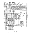
- FIG. 1 a block diagram of a video display system 100 incorporating an advance video processor 1 according to the invention.
- a host microcomputer 30 CPU
- AVDP Advance Video Processor
- the AVDP 1 is used to interface microprocessor 30 to a color video monitor 33.
- the AVDP 1 uses a dynamic RAM 31 to store the information displayed on the video screen.
- the microprocessor 30 loads the AVDP's 1 configuration registers through the 8 bit CPU to AVDP data bus 51.
- the microprocessor 30 then loads the video RAM 31 with the information that is to be displayed on a video screen 32.
- the AVDP 1 refreshes the video screen 32 independently of CPU accesses.
- the video RAM 31 is accessed by the AVDP 1 through an 8 bit address bus and 8 bit data bus.
- the AVDP 1 also supplies the necessary RAS (Row Address Strobe) and CAS (Column Address Strobe) to interface the dynamic video RAM 31 to AVDP 1.
- RAS Row Address Strobe
- CAS Column Address Strobe
- connected to the advance video processor 1 is a random access memory, video RAM 31, which is connected to the advance video processor 1 via bydirectional data bus 53, memory address bus 55 and a control lines 45.
- the graphics are displayed on either one or two possible systems, a Red, Green, and Blue (RGB) monitor 33 which is connected to the advance video processor 1 via an RGB bus 39 or a composite video monitor or TV set 35 which is connected to the advance video processor 1 via a color difference bus 41 and a video encoder or RF monitor 37. Additionally, sound is provided to the composite video monitor or TV set 35 via a sound bus 43.
- the advanced video processor 1 includes 7 basic function blocks. These include the CPU control logic 65 which handles the interface between the host microcomputer 30 and the advance video processor 1 and is the termination portion of the control lines 49, the input and output of data to data bus 51 and the providing of interrupts to the host microcomputer 30 via interrupt line 47. CPU control logic 65 enables the host microcomputer 30 to conduct five basic operations.
- CSW is the CPU 30 to AVDP 1 write select line.
- CSR is the CPU to AVDP read select line.
- CSR is active low the AVDP outputs eight bits of data onto the CDO-CD7 lines for the CPU to read.
- CSW and CSR are both active low the sound generator 69 is addressed.
- Mode determines the source or destination of a read or write transfer. Mode is generally connected to a CPU low order address line.
- FIG. 9 provides an illustration of the data transfer between the host CPU 30 to the AVDP 1.
- a video RAM control logic 67 controls the interface between the advance video processor 1 and the video RAM 31 and handles the transfer of data from the data bus 53 that is provided to the video RAM 31 at the memory address location that is provided on the memory address bus 55 in response to the control signals that are provided on the control lines 4.
- the data bus 53 is an 8 bit bidirectional bus and the memory address bus 55 is an 8 bit multiplex address bus.
- the advance video processor illustrated in Figure 1 can directly address 16K bytes, two (TMS4416s or equivalent, 32 bytes, 4 TMS4416s or equivalent, or 65K bytes 8 (TMS41664S) (all TMS parts are manufactured by Texas Instruments or equivalent) while currently providing dynamic refresh to the video RAM 31.
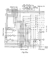
- the internal registers 63 in the embodiment shown in Figures 1 and 2 contain two read only registers, a status register and a sprite collision register in Figure 16 and forty nine write only registers illustrated in Figures 11.
- the write only registers provide the following functions. Three of the write ony registers define the mode of operation of the advance video display processor 1 and specify options such as the mode of operation and type of video signal output necessary to drive the RGB monitor 33 or the composite video mointor or TV set 35. Six of the write only registers that are contained within the internal register block 63 are designated advance video display procesor 1 to display memory address mapping reigsters and specify locations in the video RAM 31.
- One write only register is a color code register and defines colors when the video display processor 10 is operating in the text mode.
- Two separate registers are scrolling registers; one is horizontal scrolling the other is for vertical scrolling.
- One programmable interrupt register enables the advance video processor 1 to be reconfigured during a horizontal retrace interval that occurs in all television monitor signals.
- Four block move address and decament counter registers allow a defined block of video memory to be moved to another video memory location.
- Thirty two palette pilot registers define up to 16 displayable colors (from a 52 color palette) per horizontal scan lines.
- a status register contains flags for interrupts, coincidence and eleventh sprite occurance on any one horizontal line.
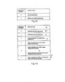
- the AVDP has a single 8-bit status register 28 which can be read by the CPU 1. The format of the status register 28 is shown in Figure 12.
- the status register contains the interrupt pending flag (F), the sprite coincidence flag (C), the eleventh sprite flag (llS), and the eleventh sprite number if one exists.
- the status register 28 may be read at any time to test the F,C and 11S status bits. Reading the status will clear the interrupt flag F. However, asynchronous reads of the status will cause the frame flag (F) bit to be reset and therefore possibly missed. Therefore the status register should only be read when the AVDP 1 interrupt is pending. It requires only one data transfer to read the status register 28.
- the F status flag in the status register is set to 1 whenever there is an interrupt pending. This bit will be set one of three ways; when a block move has completed, when a programmable interrupt is selected, or when an end of frame has occurred (Vertical Retrace Period).
- the interrupt pending flag is reset to 0 when the status register is read or by the external reset.
- the C status flag in the status register is set to a 1 if two or more sprites coincide. Coincidence occurs if any two sprites on the screen have one overlapping pixel. Transparent colored sprites, as well as those that are partially or completely off the.screen, are also considered.
- the C flag is cleared to a 0 after the status register is read or the AVDP is externally reset.
- the status register 28 should be read immediately upon powerup to ensure that the coincidence flag is reset. '
- the AVDP 1 checks each pixel position for coincidence during the generation of the pixel regardless of where it is located on the screen. This occurs every 1/60th of a second. Therefore when moving more than one pixel position during these intervals it is possible for the sprites to have multiple pixels overlapping or even to have passed completely over one another when the AVDP 1 checks for coincidence.
- the 11S status flag in the status register is set to a 1 whenever there are 11 or more sprites on a horizontal line (lines 0 to 209 depending on the mode chosen) and the frame flag (F) is equal to 0.
- the 11S status flag is cleared to a 0 after the status register is read or the AVDP is externally reset.
- the number of the llth sprite is placed into the lower 5 bits of the status register when the 11S flag is set and is valid whenever the 11S flag is 1.
- the setting of the llth sprite flag will not cause an interrupt.
- a sprite collision detection register detection register defines which group or groups of sprites have collided.
- a sprite collision register 83 is an 8 bit register that can be used to determine which groups of sprites collided.
- the sprite color byte is composed of 4 color bits, an early clock bit; and 3 remaining bits; these 3 reamining bits are used to divide the sprites into eight groups.
- Each bit in the sprite collision register 83 corresponds to one group. Therefore, whenever 2 sprites collide one or more of these bits are set.
- This register is Cleared by a CPU read to this register.
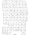
- Figure 6 shows the layout of these groups in the sprite collision register 83. It requires 3 data transfers to read this register.
- a sprite processor 10 incorporates full sprite control on the advance video display processor 1 which in the embodiment shown on a single chip.
- the sprite processor 10 includes the features which with as many as 10 sprites may occur (in the embodiment shown in Figure 1) on a single horizontal scan line. Previous video display processors were limited to only four sprites per line.
- the sprites may be multi-color or single color with each horizontal half scan line of the sprite having the option of being a different color from the sprite.
- unique sprite coincident detection is provided in the embodiment of the disclosure. A coincidence occurs if any two sprites on the display have at least one overlapping pixel. Sprite mapping necessary to provide this feature is contained in the video RAM 31.
- Graphics and text processing is provided by a graphics and text processor 60 in which the host microprocessor 30 configures the advance video display processor 1 to operate in one of the following display modes in the embodiment shown in Figure 1:
- a graphics 5 provides a full bit map of 256 x 210 pixel resolutions
- a first text mode provides 40 columns by 24 rows of text
- a second text mode provides 80 columns x 24 rows of text. All text and graphics modes with the exception of the full bit map mode designated as graphics 5 are table driven.
- a sound generator 1 provides in the embodiment shown in Figure 1 on chip sound generation that is compatible with ) the devices such as an SN764889 device manufactured by Texas Instruments Incorporated.
- the circuit provides 3 programmable tone generators; one programmable noise generator; a 120 to 100,000 HTZ frequency response and 15 programmable attenuation steps from 2dB to 28dB in steps of 2dB.
- FIG. 2 is a block diagram of the advance video processor 1 of Figure 1.
- the internal registers 63 two read-only registers and forty nine write-only registers. Included in these are color palette registers 2 which are 16 registers of 9 bits each for 16 colors.
- the color palette registers 2 are addressed by a sprite control logic 59; a first color buffer 61; a second color buffer 5 62 and a third color buffer 64 which are a part of the grphics and text processor 60; a border color register 29; and a text color register 30 which provide program colors.
- a color palette read logic 65 addresses the color palette registers 2 to place the contents contained within the color palette registers on a D-to-A logic 67 which as was discussed in conjunction with the color palette and video output logic 57 of Figure 1, provides the Red, Green and Blue colors to either the RGB monitor 33 or the different signal to the video encoded RF modulator 37.
- the output of the D-to-A logic 67 is placed on either the RGB bus 39 or the different color bus 41.
- a color palette write logic 3 controls the loading of the color codes into the color palette register 2 which includes registers R32 through R63 of Figure 11.
- the format for the palette is shown in Figures 13 and 14.
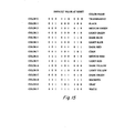
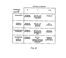
- the palette consists of sixteen 9 bit registers which allows the user to display 16 of 512 colors on the screen at one time. On an external reset the color palette is initiallized with the default values shown in Figure 15 for the color difference outputs.
- a horizontal counter, Programmable Logic Array.(PLA) 5 counts positions on the horizontal scan lines and decodes instructions based upon the beam position of the scan and provides timing to the D-to A control logic control logic 67 which is used to identify the sprite position and color.
- the vertical counter PLA 6 counts rows positions on the scan lines, decodes instructions and provides timing to the sprite register 11 as does horizontal counter PLA as to position color data. Not shown in Figure 2 is the fact that the horizontal counter PLA 5, and vertical counter PLA 6 are connected to the following logic functions.
- a color priority logic 7 decides priority of color logics between border color logic 29 text color logic 30, color buffers logic 61, and 64 and sprite control logic 59. The priority is based first on border, then on sprite when in active area, or other sprites and there are three or more dependent colors and 7 modes of operations by which the color-priority logic provides the appropriate color for the advance video display processor 1.
- a interrupt logic 8 provides interrupt to the hose CPU 30 that is based upon a timing signal interrupt to load one of the registers.
- a programmable interrupt logic 29 can provide an interrupt for any horizontal scan or line and in the embodiment shown in Figure 1 includes an eight bit register the contents of which is compared with the contents of the vertical.counter PLA 6 and provides an interrupt request to the interrupt logic 8 when there is a comparison between the contents of the two registers indicating that that scan line requires an interrupt in the proqram sequences being executed by the host CPU 30.
- the sprite control logic 59 controls the sprites fetch and checks vertical position from the vertical counter PLA 6 and causes the sprite horizontal position pattern and color data to be fetched.
- a sprite control logic 59 processes and checks all of the sprites which in the embodiment of Figure 1 includes 32 sprites to see if their positions are valid. If a sprite is to be loaded on the next scan line, the sprite control logic 59 loads the sprite number or vertical position into a sprite stack 11. The sprite stack 11 places the address of the sprite on the RAM address bus 69 for retrieval from the video RAM 31.
- a CPU register 12 interfaces the host microcomputer 30 with the video RAM 31 via the data bus 51 and 51A which is contained within the video processor 1.
- a name register 13 contains the name of the background pattern (an 8 bit number) which is used to fetch the pattern and color bytes for the next character to be displayed.
- An address register 14 addresses the video RAM 31 based upon the host microprocessor 30 instructions (whether the instruction is a read or a write instruction) and also addresses the video display processor 1, internal register 63 and color palette registers 57.
- the scroll logic includes a vertical state register 22, vertical scroll register 23, character counter 24, horizontal scroll register 25, and horizontal state register 26.
- the screen is broken up into characters.
- the character counter 24 counts the characters as the TV scan horizontally and vertically.
- the horizontal state register 26 determines which pixel of the character is being displayed.
- the vertical state counter 22 determines which row of the charater is being displayed.
- Graphics mode 5 is bit mapped and is not broken up into characters.
- the horizontal state 26, vertical state 22, and character counter 24 will count pixel by pixel as the TV scans horizontally and vertically in this mode. These counters are usxed to address the video RAM 31.
- the horizontal scroll register 25 contains an 8 bit number which determines the horizontal scroll location of the screen. At the beginning of each horizontal line the contents of the horizontal scroll register 25 is loaded into the horizontal state register 26 and character counter 24. By changing the starting position of the counters the screen can be scrolled up to 256 different horizontal positions.
- the vertical scroll register 23 contains an 8 bit number which determines the vertical scrolling of the screen. At the beginning of each screen scan, the vertical scroll register 23 is loaded into the vertical state register 22 and the character counter 24. By changing the starting position of the counters the screen can be scrolled up to 256 different vertical positions.
- the base registers 15, 16, 17, 18 defines the locations in video memory 31 where the sections of video information will be stored.
- the name base register defines the location of the name table in memory.
- the color base register 16 defines the location of the video color information.
- the sprite location register 18 defines the location of the sprite patterns, sprite colors, sprite horizontal ) position, and sprite vertical position.
- the command registers 19, 20, 21 control the mode of operation of the advanced video processor 1. The operation of each bit is explained in the Table 1 sections 3.2.1, 3.2.2, and 3.2.11.
- a status register 28 provides status via data bus 51A to the host microcomputer 30 that reflects the following interrupt information; a programmable interrupt via occured; more than 10 sprites are being used; two sprites collide; and five bits addition status bits for the llth sprit on a line.
- the CPU control logic 65 provides interrupts to the host microcomputer 30 and receives the write commands, the read commands, and mode commands indicating operation; if writing or reading to the video internal registers 63 or video RAMs 31.
- the blank name registers 27 (2) 16 bit registers are used to move data from one section of memory to another section of memory. One register contains the number of bytes to be moved; the other register contains the read memory location. The write memory destination is located in the address register 14.
- the color buffers 60 contain 3 bytes of pattern plane color information.
- Buffer 64 contains the colors which are ready to be loaded onto the color Buss 86.
- This buffer contains 1 byte of information or (2) 4 bit colors.
- the LSB nibble is the first color pixel to be displayed and the MSB nibble is the second color pixel to be displayed.
- Buffers 61 and 62 are temporary storage buffers which will be loaded into buffer 64.
- the pattern buffer 84 contains the 1's and 0's which will determine which color in buffer 64 will be displayed.
- the pattern buffer 84 is loaded into the pattern shift register 86 and shifted out serially.
- the output of the shift register 86 loads the colors from buffer 64 onto the color buss 86 depending on the color priority logic.
- the sprite registers 100 contain the sprite horizontal pointer 82, the sprite pattern register 81, the sprite color register 80, and the sprite coincidence selection logic 70. This is repeated 10 times for 10 sprites per horizontal line.
- the sprite horizontal counter 82 is loaded with the horizontal sprite position and decrements to the value of zero. Then the sprite pattern register 81 begins shifting bits out serially. 1's load this sprite color onto the color buss 86 and 0's are not used.
- the sprite color register 80 contains 4 bits for the sprite color, 1 bit for early clock, and 3 bits to indicate the sprite group.
- the sprite coincidence detection logic 70 determines if two or more sprites are shifting 1's out of the sprite pattern register 80 at the same time. If this happens 2 or more sprites have collided on the screen.
- the sprite groups are decoded from the three bits stored in the 10 sprite color registers 80, and the bits corresponding to the sprite groups are set in the sprite'coincidence register 83. If the sprites are in the border area and will not be displayed, the bits will not be set.
- the three bits in the sprite color register 80 can be decoded into 8 groups, each group corresponds to a bit in the sprite coincidence register 83.
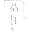
- the coincidence detector of Figures 1 and 2 is useful in the application of the invention to video games; for example a space game in which a space ship 110 which is defined as sprite 1 belonging to group 1, and a plurality of rocket ships which are defined as sprites 2, 3 and 4, all assigned to group 2, a flying saucer 11 which is sprite 8 of group 4 and a plurality of meteors 115, 116 and 117 all are sprites belonging to group 3 are used to implement the game. If one of the rocket ships 112 a, b or c which are in group 2 collide with one another, a coincidence will be deteced and bit 2 of the sprite coincidence register.53 will be set .
- the spaceship 110 collides with one of the missiles 112, a coincidence will be detected, and bits 1 and 2 of the sprite coincidence register 83 will be set.
- the host CPU 30 can check to see if the spaceship 10 has collided with another object by reading the sprite coincidence register 83 and checking bit 1.
- FIG. 5 demonstrates multicolor sprites.
- Sprites can have a different color on each horizontal line.
- Sprite (1) which contains the hat, eyes, nose, and mouth is only one sprite, even though there are four different colors.
- Sprite (2) is the face of the sprite and has to be drawn as a separate sprite since it is on the same horizontal lines as the eyes, nose, and mouth.
- sprite 1 and sprite 2 are combined together the sprite 129 is created.
- the sprite coincidence detector, 70 of Figure 2 will provide to the sprite register 83 when one of the groups
- Figure 7 combines the necessary processing on a single chip that allows both grahics and alphanumeric data (video-text) to be generated.
- two way communication is provided in a video text example over standard lines 237 using a modem 235, a data access arrangement 234, and a UART 233.
- the host CPU 30 has additional interface to a ROM memory 231 and a RAM memory 232, as well as operator interface by a keyboard 236.
- the Advance Video Data Processor is connected to four RAM's that represent the video RAM 31, and includes an A RAM, B RAM, C RAM, and D RAM as illustrated in Figure 7.
- the use of the four RAMs which in the preferred embodiment are TMS44116s manufactured by Texas Instruments, provides the memory necessary for the video data storage.
- the video data is sequenced out by the advance video display processor 1 and then encoded by the video encoder 37 to dot data for each horizontal scan line.
- the information can then be viewed on the TV set 35.
- the video display processor 1 provides all the video information and synchronization required to refresh and display the images on the TV set 35.
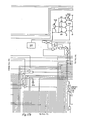
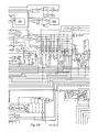
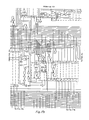
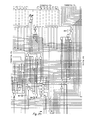
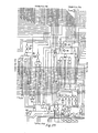
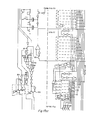
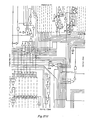
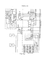
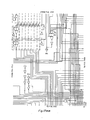
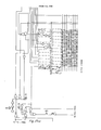
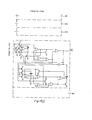
- Figure 17 is a schematic diagram of the implementation of the Advance Video Processor 1 with field effect transistors technology.
Landscapes
- Engineering & Computer Science (AREA)
- Physics & Mathematics (AREA)
- Computer Hardware Design (AREA)
- General Physics & Mathematics (AREA)
- Theoretical Computer Science (AREA)
- Controls And Circuits For Display Device (AREA)
- Processing Or Creating Images (AREA)
- Digital Computer Display Output (AREA)
- Closed-Circuit Television Systems (AREA)
Applications Claiming Priority (2)
| Application Number | Priority Date | Filing Date | Title |
|---|---|---|---|
| US60068884A | 1984-04-16 | 1984-04-16 | |
| US600688 | 1984-04-16 |
Publications (2)
| Publication Number | Publication Date |
|---|---|
| EP0165665A2 true EP0165665A2 (fr) | 1985-12-27 |
| EP0165665A3 EP0165665A3 (fr) | 1989-02-22 |
Family
ID=24404669
Family Applications (1)
| Application Number | Title | Priority Date | Filing Date |
|---|---|---|---|
| EP85302464A Withdrawn EP0165665A3 (fr) | 1984-04-16 | 1985-04-09 | Détecteur de collisions entre images mobiles |
Country Status (2)
| Country | Link |
|---|---|
| EP (1) | EP0165665A3 (fr) |
| JP (1) | JPS6122395A (fr) |
Cited By (1)
| Publication number | Priority date | Publication date | Assignee | Title |
|---|---|---|---|---|
| EP0318517B1 (fr) * | 1986-07-18 | 1996-02-28 | Escom Ag | Circuits generateurs d'affichage pour systeme d'ordinateur personnel |
Family Cites Families (5)
| Publication number | Priority date | Publication date | Assignee | Title |
|---|---|---|---|---|
| US4119955A (en) * | 1977-03-24 | 1978-10-10 | Intel Corporation | Circuit for display, such as video game display |
| JPS6057355B2 (ja) * | 1978-10-17 | 1985-12-14 | 株式会社ナムコ | Crtデイスプレイの移動体と障害物の衝突検出方法 |
| US4296476A (en) * | 1979-01-08 | 1981-10-20 | Atari, Inc. | Data processing system with programmable graphics generator |
| US4243984A (en) * | 1979-03-08 | 1981-01-06 | Texas Instruments Incorporated | Video display processor |
| NL8101339A (nl) * | 1981-03-19 | 1982-10-18 | Philips Nv | Inrichting voor het afbeelden van digitale informatie met selektiemogelijkheid van beeldpagina's en/of resolutie uitbreiding. |
-
1985
- 1985-04-09 EP EP85302464A patent/EP0165665A3/fr not_active Withdrawn
- 1985-04-16 JP JP60081207A patent/JPS6122395A/ja active Pending
Cited By (1)
| Publication number | Priority date | Publication date | Assignee | Title |
|---|---|---|---|---|
| EP0318517B1 (fr) * | 1986-07-18 | 1996-02-28 | Escom Ag | Circuits generateurs d'affichage pour systeme d'ordinateur personnel |
Also Published As
| Publication number | Publication date |
|---|---|
| JPS6122395A (ja) | 1986-01-30 |
| EP0165665A3 (fr) | 1989-02-22 |
Similar Documents
| Publication | Publication Date | Title |
|---|---|---|
| US5089811A (en) | Advanced video processor having a color palette | |
| EP0071725B1 (fr) | Méthode de décalage de textes et de données graphiques dans des fenêtres sélectionnées sur un affichage graphique | |
| EP0071744B1 (fr) | Méthode de fonctionnement d'un système de calcul pour écrire des caractères alphanumériques sur un affichage graphique | |
| US4823120A (en) | Enhanced video graphics controller | |
| KR960012990B1 (ko) | 비트 맵 영상 데이타를 블럭 전송하기 위한 퍼스널 컴퓨터 시스템 및 그 사용 방법 | |
| US5696540A (en) | Display controller | |
| EP0012793B1 (fr) | Procédé d'affichage d'images graphiques par un dispositif d'affichage de trame et dispositif de mise en oeuvre du procédé | |
| US4628467A (en) | Video display control system | |
| US5453763A (en) | Still picture display apparatus and external memory cartridge used therefor | |
| WO1988001778A1 (fr) | Appareil et procede d'affichage monochrome/multicolor et images superposees | |
| US5086295A (en) | Apparatus for increasing color and spatial resolutions of a raster graphics system | |
| US4616220A (en) | Graphics display comparator for multiple bit plane graphics controller | |
| US4804948A (en) | Video display control system | |
| EP0215984B1 (fr) | Appareil d'affichage graphique avec mémoire tampon-bit et caractère-graphique combiné | |
| US4763118A (en) | Graphic display system for personal computer | |
| EP0159851B1 (fr) | Processeur vidéo avancé avec commande de décalage par hardware | |
| US5642138A (en) | Display control system using a different clock in the graphics mode from that in the text mode in accessing an image memory | |
| EP0360530A2 (fr) | Dispositif de commande d'affichage programmable à formats multiples | |
| EP0165665A2 (fr) | Détecteur de collisions entre images mobiles | |
| US5376949A (en) | Display system with graphics cursor | |
| KR960003072B1 (ko) | 폰트 데이타 처리장치 | |
| KR0175142B1 (ko) | 정지화상 표시장치 및 그것에 이용되는 외부 메모리 카트리지 | |
| JP2898482B2 (ja) | コンピュータゲーム装置 | |
| EP0272006A2 (fr) | Contrôleur de visualisation pour les appareils de traitement des données | |
| JPH0661036B2 (ja) | 図形表示装置 |
Legal Events
| Date | Code | Title | Description |
|---|---|---|---|
| PUAI | Public reference made under article 153(3) epc to a published international application that has entered the european phase |
Free format text: ORIGINAL CODE: 0009012 |
|
| AK | Designated contracting states |
Designated state(s): DE FR GB |
|
| PUAL | Search report despatched |
Free format text: ORIGINAL CODE: 0009013 |
|
| AK | Designated contracting states |
Kind code of ref document: A3 Designated state(s): DE FR GB |
|
| 17P | Request for examination filed |
Effective date: 19890724 |
|
| 17Q | First examination report despatched |
Effective date: 19910213 |
|
| STAA | Information on the status of an ep patent application or granted ep patent |
Free format text: STATUS: THE APPLICATION IS DEEMED TO BE WITHDRAWN |
|
| 18D | Application deemed to be withdrawn |
Effective date: 19910826 |
|
| RIN1 | Information on inventor provided before grant (corrected) |
Inventor name: LEACH, JERALD G. |