EP0166328A2 - Procédé et dispositif pour produire l'image d'un objet ou du diagramme de diffraction d'un objet par filtrage d'énergie des électrons avec un microscope électronique à transmission - Google Patents
Procédé et dispositif pour produire l'image d'un objet ou du diagramme de diffraction d'un objet par filtrage d'énergie des électrons avec un microscope électronique à transmission Download PDFInfo
- Publication number
- EP0166328A2 EP0166328A2 EP85107385A EP85107385A EP0166328A2 EP 0166328 A2 EP0166328 A2 EP 0166328A2 EP 85107385 A EP85107385 A EP 85107385A EP 85107385 A EP85107385 A EP 85107385A EP 0166328 A2 EP0166328 A2 EP 0166328A2
- Authority
- EP
- European Patent Office
- Prior art keywords
- spectrometer
- image
- always
- imaging
- crossover
- Prior art date
- Legal status (The legal status is an assumption and is not a legal conclusion. Google has not performed a legal analysis and makes no representation as to the accuracy of the status listed.)
- Granted
Links
Images


Classifications
-
- H—ELECTRICITY
- H01—ELECTRIC ELEMENTS
- H01J—ELECTRIC DISCHARGE TUBES OR DISCHARGE LAMPS
- H01J37/00—Discharge tubes with provision for introducing objects or material to be exposed to the discharge, e.g. for the purpose of examination or processing thereof
- H01J37/02—Details
- H01J37/04—Arrangements of electrodes and associated parts for generating or controlling the discharge, e.g. electron-optical arrangement or ion-optical arrangement
- H01J37/05—Electron or ion-optical arrangements for separating electrons or ions according to their energy or mass
-
- H—ELECTRICITY
- H01—ELECTRIC ELEMENTS
- H01J—ELECTRIC DISCHARGE TUBES OR DISCHARGE LAMPS
- H01J37/00—Discharge tubes with provision for introducing objects or material to be exposed to the discharge, e.g. for the purpose of examination or processing thereof
- H01J37/26—Electron or ion microscopes; Electron or ion diffraction tubes
Definitions
- the present invention relates to a method and an arrangement for electron energy-filtered imaging of an object with a transmission electron microscope, in which the electron beams emanating from an electron source illuminate the object, the object is imaged from a first imaging stage into the input image plane of an imaging electron energy spectrometer and simultaneously the electron source is mapped into the input crossover point of the spectrometer, in which electrons of a selectable energy range are also filtered out in the spectrometer and the filtered object image is imaged from the output image plane of the spectrometer into the end image plane.
- the present invention further relates to a corresponding method for object diffraction patterns.
- a major advantage of a transmission electron microscope with an imaging electron energy spectrometer is that the contrast of the object image is much better than in conventional devices by the selection of electrons of a certain energy range. This can be seen most clearly in the case of non-contrasted, very thin specimens with a chosen energy loss ( ⁇ E) in the range from approx. 100 to 200 eV.
- ⁇ E energy loss
- Another significant advantage of a transmission electron microscope with an imaging electron energy spectrometer is the possibility to carry out element-specific object images, ie element distribution images, simultaneously from a relatively large object area in that the energy range transmitted by the electron energy spectrometer has an element-specific interaction corresponds to the transmitted electrons with the object, for example a K, L, M absorption in the atomic shell. It can also be used for qualitative purposes and when measuring the intensity ratios and subtracting the surface quantitative distribution images of elements in thin objects ( ⁇ 30 nm) with very high spatial resolution ( ⁇ 0.5 nm) and highest detection sensitivity ( ⁇ 2.10 -21 g) are obtained that have not been achieved with any other analytical technique. Highest spatial resolution and detection sensitivity of elements are of great importance both for biological and medical research and for materials science.
- an imaging electron energy spectrometer produces sharper images of the diffraction pattern by masking out inelastically scattered electrons.
- an electron microscope is known which not only enables filtering of the object image but also of the diffraction diagram image.
- an enlarged image of the diffraction diagram is generated by a first imaging stage from three lenses in the input image plane of the spectrometer (denoted B2 in the PS) and an object image in the input crossover plane (denoted B1 in the PS).
- the image position and the image of the electron source (crossover) in front of the spectrometer shift.
- the Crossover placed in the right place for the actual spectrometer; the image position is corrected by refocusing the objective lens.
- the same procedure is required if the rear focal plane of the objective is imaged in the spectrometer by imaging the electron diffraction diagram by changing the excitation of the 1st and 2nd intermediate lens.
- the imaging aperture of the spectrometer is limited by an area stop in the 1st intermediate image after the objective lens.
- the present invention is therefore based on the object of achieving the largest possible magnification range in a transmission electron microscope with an imaging electron energy spectrometer, without readjustments (refocusing) being necessary when changing the magnification.
- a magnification-independent spectrometer aperture diaphragm is to be created for the selection of the energy resolution with optimal adaptation to the image-delimiting surface of the respective detector.
- image energy-filtered diffraction diagrams with a magnification pre-variation of at least 3: 1.
- the invention also has the task of improving the energy resolution of the electron energy spectrometer with a prism-mirror-prism system.
- the present object is achieved on the basis of a method according to the preamble of claim 1 according to the invention in that with the first imaging stage the object which remains in the unchanged position is always imaged in the input image plane of the spectrometer with a magnification variation of at least 8: 1 and with little distortion and at the same time that Image of the electron source is always imaged in the input crossover point of the spectrometer and that with the second imaging stage the output image plane of the spectrometer is imaged with a constant magnification in the end image plane, the constant magnification being adapted only to the image-delimiting surface of the respective detector.
- the first imaging stage always shows the diffraction diagram of the object that remains unchanged with a magnification variation of at least 3: 1 in the input image plane of the spectrometer and at the same time the image of the object always in the input crossover plane of the spectrometer.
- the second mapping level the Output image plane of the spectrometer mapped with a constant magnification in the final image plane, the constant magnification being adapted only to the image-delimiting surface of the detector.
- the first imaging stage generates four intermediate images of the object, of which the fourth intermediate image always lies in the input image plane of the spectrometer, and at the same time four crossovers (intermediate images of the electron source), of which the fourth crossover always lies in the input crossover point of the spectrometer.
- the second intermediate image is real or virtual, while all other intermediate images are always real; in addition, the third crossover is real or virtual, while all other crossovers are always real.
- the first intermediate image is always virtual
- the second intermediate image is real or virtual, while the last two intermediate images are always real; in addition, the second and / or third crossover is real or virtual, while the first and last crossover are always real.
- the first imaging stage For object diffraction diagrams, the first imaging stage generates the diffraction diagram and three intermediate images of the diffraction diagram, of which the third intermediate image always lies in the input image plane of the spectrometer, and all intermediate images being real. At the same time, the first imaging stage generates four intermediate images of the object, of which the fourth intermediate image is always in the input crossover plane of the spectrometer, the second intermediate image being always virtual, while all other intermediate images are always real.
- the first imaging stage is constructed from four electron-optical lens groups which are connected to a power supply unit in which the required excitation current is defined for each magnification stage and for each lens.
- Each lens group can consist of one or more electron-optical lenses.
- the spectrometer aperture diaphragm is arranged between the input crossover and the input image plane of the spectrometer as close as possible to the input image plane and has exchangeable circular openings for the choice of the spectrometer aperture or the energy resolution.
- 10 denotes a transmission electron microscope, the electron source 11 of which consists of a cathode 11a and an acceleration electrode 11b.
- the lenses 12a and 12b form the condenser system; 12c is a condenser diaphragm.
- the imaged object 13 is removably disposed within the objective lens and 0 is increased by these in an intermediate image plane B l, eg at medium to high magnifications in the range aperture 13a imaged. From there, the intermediate image is imaged by the further lenses P 1 , P 2 , P 3 of the first imaging stage 14 into the imaging electron energy spectrometer 15, in front of which the aperture diaphragm 42 is arranged.
- the subsequent second imaging stage 16 forms the output image of the spectrometer 15 into the final image plane 17.
- a fluorescent screen 17a, a camera with films 17b or possibly an electronic detector 17c is normally arranged there.
- the spectrometer 15 consists of a magnetic prism 20, which is generated by a magnet with two pole shoes, the end faces of which have the shape of the prism 20 and lie closely below and above the plane of the drawing. It has two mirror-symmetrical effective areas 21 and 22 and an electrostatic mirror 23.
- the electron beam 25 incident in the optical axis 24 with the aperture angle ⁇ is deflected by the upper effective area 21 by approximately 90 ° to the mirror 23, at which it is reflected.
- the electron beam 25 is then deflected again in the lower effective range 22 by approximately 90 ° and leaves the spectrometer in the direction of the optical axis 24.
- the exact deflection angle depends in each case on the energy of the electrons, so that in the dispersion plane C A a spectrum of the energy of the electrons transmitted by the object, a part of which can be hidden by split jaws 43b, 43c.
- the spectrometer 15 maps the input image plane B E into the output image plane B A on a scale of 1: 1 and the input crossover point C E into the dispersion plane C A.
- the image of the beam source 11 into the input crossover point C, E and the image of the object 13 in the input image plane B E is imaged by the arranged in front of the spectrometer electron optical lenses - and that in Object diffraction diagrams, the image of the beam source 11 in the input image plane B E and the object image in the input crossover plane C E 'is mapped. Only if these conditions are met exactly will the spectrometer provide achromatic imaging and optimal energy filtering.
- the first imaging stage 14 is constructed according to the invention from four electron-optical lens groups 0, P 1 , P 2 , P 3 , each Lens group can consist of one or more lenses and the switching to different magnifications and from object image to diffraction image and vice versa takes place through different excitations of the electromagnetic coils of lens groups 0, P 1 , P 2 , P 3 .
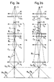
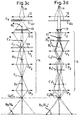
- the imaging and illumination beam paths present at different magnification ranges for object imaging and with diffraction imaging are shown in FIGS. 3a to 3d.
- FIG. 3a shows the illumination beam path in dashed lines and the imaging beam path in solid lines for an object point on the optical axis for a total magnification of approximately 25,000 x to 250,000 x, or for an enlargement by the first imaging stage 14 of approximately 300 x to 3,000 x.
- the object 13 is illuminated by the condenser system 12 with an approximately parallel electron beam, the diameter of which is determined by the condenser diaphragm 12c.
- the first lens group 0 generates a real intermediate image B 1 from the object 13 and the real intermediate image (crossover) C 1 from the electron source 11.
- the second lens system P 1 generates the real intermediate image B 2 and the real crossover C 2 ; the third lens system P 2 generates the real intermediate image B 3 and the real crossover C 3 .
- the lens system P 3 generates the real intermediate image B 4 of the object 13 in the input plane B E of the spectrometer 15 and the real crossover C 4 in the input crossover point C E of the spectrometer 15.
- This imaging and illuminating beam path differs from known beam paths in that up to an intermediate image before the last imaging stage they contain a smaller number of lenses or lens systems and that their last crossover point before the intermediate image has no defined, constant position. It is crucial that the same first imaging stage 14, consisting of the lens groups 0, P 1 , p 21 P 3, also generate the beam paths shown in FIGS. 3b to 3d.
- FIG. 3b shows the illumination beam path in dashed lines and the imaging beam path in solid lines for a total magnification of 2,500 x to 25,000 x, or for an enlargement by the first imaging stage 14 of approx. 30 x to 300 x.
- the object 13 is illuminated in accordance with FIG. 3a and the first lens group 0 again generates a real intermediate image B, the object 13 and a real one Crossover C T.
- the second lens group P 1 is so weakly excited that it produces a real crossover C 2 , but only a virtual intermediate image 8 2 * of the object 13.
- the third lens group P 2 then becomes a real intermediate image B 3 of the object 13, but only a virtual crossover C 3 * is generated.
- the fourth lens group P 3 finally generates a real intermediate image B 4 of the object 13 in the input image plane B E of the spectrometer 15 and a real crossover C 4 in the input crossover point C E of the spectrometer 15.
- the imaging and illumination beam path shown in FIG. 3b also differs from known beam paths in that they contain a smaller number of lenses or lens systems up to an intermediate image before the last imaging stage and that their last crossover point in front of the intermediate image has no defined, constant position.
- FIG. 3c shows the illumination beam path in dashed lines and, when drawn out, the imaging beam path for a total magnification of approximately 100 x to 2,000 x, or for an enlargement of the first imaging stage 14 of approximately 1.2 x to 24 x.
- the beam paths up to the intermediate image B 2 correspond to DE-PS 27 42 264.
- the condenser lens is excited in such a way that an intermediate image (Crossover) designated by C o
- the beam source is already in front of the object 13, specifically in or near the condenser diaphragm 12c.
- the first lens group 0 is excited so weakly that the next crossover C 1 lies in the area diaphragm 13a and only a virtual image B 1 * is produced from the object 13.
- the second lens group P 1 generates a real intermediate image B 2 of the object 13 and a virtual crossover C 2 * .
- a real intermediate image are B 3 and a real crossover C 3 produces and the fourth lens group P 3 is a real intermediate image are B 4 of the object 13 in the input image plane B E of the spectrometer 15 and a real crossover C 4 in Crossover entry point C E of the spectrometer generated.
- FIG. 3d shows the beam paths for the imaging of electron diffraction diagrams.
- the illumination of the sample 13 again takes place in accordance with FIGS. 3a and 3b.
- the lens group 0 generates the object diffraction diagram C 1 'and the object image B 1 ' from the electrons scattered on the sample 13.
- Ent electrons not scattered by object 13 speaks the extended beam path and the dash-dotted beam paths correspond to the electrons scattered by the object 13.
- the second lens group P 1 produced by the object diffraction pattern C l 'the diffraction intermediate image C2' and the object B image 1 ', the virtual intermediate image B 2 ⁇ *.
- the third lens group P 2 then generates a real intermediate diffraction image C 3 'and a real object intermediate image B 3 ', which are imaged by the fourth lens group P 3 into the input image plane B E and the input crossover plane C E 'of the spectrometer.
- magnification levels are possible for each of the beam profiles shown in FIGS. 3a to 3d. Their number is simply a question of effort and benefit. It is crucial that with the beam paths for object images shown in FIGS. 3a and 3b, a magnification variation of approximately 100: 1 is possible with any desired gradation with a defined and constant position of the intermediate image B 4 and the crossover point C 4 . This magnification variation is expanded to approximately 2,500: 1 by the beam paths described in FIG. 3c. The beam paths shown in FIG. 3d allow a magnification variation of 20: 1 with the same first imaging stage 14 for diffraction diagrams.
- Each of the lens groups labeled 0, P 1 , P 2 and P 3 can consist of one or more lenses.
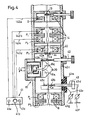
- the various magnification levels are set via the control unit denoted by 41 in FIG. This is connected via cables 42a to 42d to the coils of the lenses 0, P 1 , p 21 P 3 , which supply the lenses with the excitation currents necessary for the magnification stages.
- the control unit 41 has a magnification step switch 41b, with which the lens excitation currents are generated at each magnification step for each lens by means of an analog control, for example by switching over setpoint resistances.
- an analog control for example by switching over setpoint resistances.
- E-PROM electronic read-only memory
- the control unit 41 also has a switch 41c for switching from object image to diffraction image and vice versa, and a balancing controller 41a for focusing (focusing) the object.
- FIG. 4 also schematically shows the structure of the aperture diaphragm 42 for the spectrometer 15.
- This aperture diaphragm 42 should ideally sit in the input image plane B E of the spectrometer. Because this is hardly possible due to the very small distance between the pole pieces of the prism 20 for mechanical reasons , the aperture diaphragm 42 is arranged as close as possible in front of the prism 20, which is sufficient in practice because, due to the small extent of the image of the electron source at the input crossover point CE, there is always a sharply delimited shadow image of the aperture diaphragm 42 in the input image plane B E.
- the entrance aperture diaphragm 42 consists of a vacuum-tight passage 42c through the microscope column 40 and circular diaphragms 42a, 42b with different diameters, which can optionally be brought into the beam path.
- the magnification is adjusted by the first imaging stage 14 in front of the spectrometer aperture 42 and with the second imaging stage 16 after the spectrometer 15 there is only a constant magnification which is only adapted to the image-limiting surface of the detector 17a, 17b, 17c, the effect is the aperture diaphragm 42 is independent of magnification.
- the circular diaphragms 42a, 42b with different diameters enable the setting of different aperture angles ⁇ .
- the energy resolution of the spectrometer in the dispersion plane C A is still aperture-dependent.
- the setting option of different aperture angles therefore enables a change in the energy resolution of the spectrometer, so that it can either be optimally adapted to the image-limiting surface of the respective detector 17b, 17c, the energy resolution being ⁇ 15 eV for ⁇ ⁇ 10 mrad, or by choosing one very small (image-limiting) aperture, the energy resolution can be improved up to the energy width of the beam source 11, ie for a thermal beam source it can be reduced to the minimum energy width of 0.8 eV.
- FIG. 4 also schematically shows the slit diaphragm 43, which is arranged in the dispersion plane C A of the spectrometer 15.
- the slit diaphragm 43 has a vacuum-tight passage through an insulator 43a, which sits in the microscope column 40.
- the two split jaws 43b and 43c can be moved together and against each other; they are insulated from one another and connected to current measuring devices 43f, 43g outside the microscope column 40 by separate lines 43d, 43e. With this arrangement, part of the spectrum for object imaging can be masked out and the electron current from different parts of the spectrum can be measured directly.
- a deflection system 44 is shown in FIG. 4, which is arranged in the input crossover plane C E 'of the spectrometer 15. With this deflection system 44, the electron beam emerging from the first imaging stage 14 can be aligned precisely in the optical axis 24 (FIG. 2) of the spectrometer 15 without affecting any other imaging parameters.
- the second imaging stage 16 is made up of at least two projective lenses P 4 , P 5 , which can be changed independently of one another in their lens power.
- the first lens P 4 forms either the output image plane B A or the dispersion plane C A in the object plane of the second lens P 5 .
- the second lens P 5 is used to optimally adapt the aperture diaphragm or to adapt the spectrum range to the different final image formats, for example to different photo formats from different cameras or to the size of a detector system.
- the latter can be, for example, a Faraday cage, a scintillator / photomultiplier combination, a CCD array or a see-through fluorescent screen with a television tube connected downstream.
- first and second imaging stage distances and lens focal lengths are given below, an electron-optical lens being provided for each lens system.
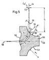
- FIG. 5 shows the parameters necessary for identifying a particularly favorable design of a prism-mirror-prism spectrometer.
- the created area 50 indicates the shape of the end faces of the pole shoes of the magnet, between which the electron beam 25 passes.
- E denotes the angle between the axis 24 of the incident electron beam 25 and the surface normal 54 at the entry point 55 into the prism, and R denotes the path radius of the electron beam 25 deflected in the prism.
- the distance of the entry point 55 from the entrance crossover point C E is called the focal length f 1 designated.
- the entrance surface 51 has the shape of a concave circular section with the radius R i .
- the exit surface 52 to the mirror has the shape of a convex circular section with the radius R 2 .
- This curved surface is 52 at the same time the entrance surface of the reflected electron beam, which exits the prism through the surface 53.
- the concave exit surface 53 again has the radius of curvature R 1 .
- the curved entry and exit surfaces 51, 52, 53 significantly improve the focusing properties of the spectrometer both in the plane of the drawing and perpendicular to it, so that the 2nd order aberrations can be neglected up to apertures ⁇ of approximately 10 mrad.
- a particularly favorable dimensioning range for the radii R 1 and R 2 is specified in claim 12.
- Circular boundaries of the pole shoes - and thus the entry and exit surfaces - have the advantage that they are easy to manufacture.
- a further improvement of the focusing properties is possible through the non-circularly curved boundaries of the pole pieces.
Landscapes
- Chemical & Material Sciences (AREA)
- Analytical Chemistry (AREA)
- Analysing Materials By The Use Of Radiation (AREA)
Applications Claiming Priority (2)
| Application Number | Priority Date | Filing Date | Title |
|---|---|---|---|
| DE3423149 | 1984-06-22 | ||
| DE19843423149 DE3423149A1 (de) | 1984-06-22 | 1984-06-22 | Verfahren und anordnung zur elektronenenergiegefilterten abbildung eines objektes oder eines objektbeugungsdiagrammes mit einem transmissions-elektronenmikroskop |
Publications (3)
| Publication Number | Publication Date |
|---|---|
| EP0166328A2 true EP0166328A2 (fr) | 1986-01-02 |
| EP0166328A3 EP0166328A3 (en) | 1986-12-30 |
| EP0166328B1 EP0166328B1 (fr) | 1991-01-09 |
Family
ID=6238943
Family Applications (1)
| Application Number | Title | Priority Date | Filing Date |
|---|---|---|---|
| EP85107385A Expired - Lifetime EP0166328B1 (fr) | 1984-06-22 | 1985-06-14 | Procédé et dispositif pour produire l'image d'un objet ou du diagramme de diffraction d'un objet par filtrage d'énergie des électrons avec un microscope électronique à transmission |
Country Status (4)
| Country | Link |
|---|---|
| US (1) | US4812652A (fr) |
| EP (1) | EP0166328B1 (fr) |
| JP (1) | JPH0642358B2 (fr) |
| DE (2) | DE3423149A1 (fr) |
Cited By (1)
| Publication number | Priority date | Publication date | Assignee | Title |
|---|---|---|---|---|
| US4958074A (en) * | 1987-07-13 | 1990-09-18 | Oesterreichische Investitionskredit Aktiengesellschaft | Apparatus and method for inspecting a mask |
Families Citing this family (30)
| Publication number | Priority date | Publication date | Assignee | Title |
|---|---|---|---|---|
| NL8801163A (nl) * | 1988-05-04 | 1989-12-01 | Philips Nv | Auger spectrometrie. |
| JPH0760661B2 (ja) * | 1988-07-22 | 1995-06-28 | 株式会社日立製作所 | 電子顕微鏡 |
| DE3825103A1 (de) * | 1988-07-23 | 1990-01-25 | Zeiss Carl Fa | Verfahren zum beleuchten eines objektes in einem transmissions-elektronenmikroskop |
| DE69213157T2 (de) * | 1991-10-24 | 1997-03-06 | Philips Electronics Nv | Elektronenstrahlvorrichtung |
| DE69529987T2 (de) * | 1994-07-15 | 2004-01-15 | Hitachi Ltd | Elektronischer energiefilter |
| JP3139920B2 (ja) * | 1994-07-25 | 2001-03-05 | 株式会社日立製作所 | エネルギフィルタおよびこれを備えた透過電子顕微鏡 |
| US5578823A (en) * | 1994-12-16 | 1996-11-26 | Hitachi, Ltd. | Transmission electron microscope and method of observing element distribution by using the same |
| DE19543652C1 (de) * | 1995-11-23 | 1997-01-09 | Focus Gmbh | Reflexionselektronenmikroskop |
| US5798524A (en) * | 1996-08-07 | 1998-08-25 | Gatan, Inc. | Automated adjustment of an energy filtering transmission electron microscope |
| US6184524B1 (en) | 1996-08-07 | 2001-02-06 | Gatan, Inc. | Automated set up of an energy filtering transmission electron microscope |
| FR2753303B1 (fr) * | 1996-09-12 | 1998-12-04 | Centre Nat Rech Scient | Filtre d'energie, microscope electronique a transmission et procede de filtrage d'energie associe |
| JP3518271B2 (ja) * | 1997-08-28 | 2004-04-12 | 株式会社日立製作所 | エネルギーフィルタおよびこれを備えた電子顕微鏡 |
| DE19860988B4 (de) * | 1997-08-28 | 2007-12-13 | Hitachi, Ltd. | Elektronenmikroskop mit Energiefilter |
| DE19738070A1 (de) * | 1997-09-01 | 1999-03-04 | Leo Elektronenmikroskopie Gmbh | Energiefilter, insbesondere für ein Elektronenmikroskop |
| DE19746785A1 (de) * | 1997-10-23 | 1999-04-29 | Leo Elektronenmikroskopie Gmbh | Teilchenstrahlgerät mit Energiefilter |
| JP3571528B2 (ja) | 1998-04-10 | 2004-09-29 | 日本電子株式会社 | エネルギーフィルタを備える電子顕微鏡 |
| DE10020382A1 (de) * | 2000-04-26 | 2001-10-31 | Ceos Gmbh | Strahlerzeugungssystem für Elektronen oder Ionenstrahlen hoher Monochromasie oder hoher Stromdichte |
| US6548810B2 (en) * | 2001-08-01 | 2003-04-15 | The University Of Chicago | Scanning confocal electron microscope |
| DE10211977A1 (de) * | 2002-03-18 | 2003-10-02 | Leo Elektronenmikroskopie Gmbh | Rasterelektronenmikroskop |
| JP3789104B2 (ja) * | 2002-05-13 | 2006-06-21 | 株式会社日立ハイテクノロジーズ | 元素分布観察方法及び装置 |
| JP4048925B2 (ja) * | 2002-11-18 | 2008-02-20 | 株式会社日立製作所 | 電子顕微鏡 |
| JP4399471B2 (ja) * | 2007-02-28 | 2010-01-13 | 株式会社日立ハイテクノロジーズ | 電子分光器を備えた透過型電子顕微鏡 |
| DE102008064696B4 (de) * | 2008-12-23 | 2022-01-27 | Carl Zeiss Microscopy Gmbh | Teilchenoptische Vorrichtung mit Magnetanordnung und ihre Verwendung zum Abbilden oder Beleuchten |
| US8598526B2 (en) | 2010-03-01 | 2013-12-03 | Carl Zeiss Microscopy Gmbh | Transmission electron microscope |
| JP2013096900A (ja) * | 2011-11-02 | 2013-05-20 | Jeol Ltd | 透過電子顕微鏡および透過電子顕微鏡像の観察方法 |
| EP3070732A1 (fr) * | 2015-03-18 | 2016-09-21 | Fei Company | Appareil et procédé permettant de réaliser une spectroscopie dans un microscope à particules chargées en transmission |
| KR101815850B1 (ko) * | 2016-03-23 | 2018-01-30 | 한국표준과학연구원 | 모노크로미터 및 이를 구비한 하전입자선 장치 |
| KR101773861B1 (ko) * | 2016-05-20 | 2017-09-01 | 한국표준과학연구원 | 모노크로미터를 구비한 전자선장치 |
| WO2019021420A1 (fr) * | 2017-07-27 | 2019-01-31 | 株式会社日立ハイテクノロジーズ | Dispositif à faisceau de particules chargées et procédé d'ajustement du dispositif à faisceau de particules chargées |
| US20260038764A1 (en) * | 2024-07-30 | 2026-02-05 | Fei Company | Methods of operating a charged particle microscope system including a beam deflector and associated systems |
Family Cites Families (8)
| Publication number | Priority date | Publication date | Assignee | Title |
|---|---|---|---|---|
| DE1049988B (fr) * | 1953-09-04 | |||
| FR2055772A1 (fr) * | 1969-08-13 | 1971-04-30 | Sopelem | |
| US3715582A (en) * | 1970-02-13 | 1973-02-06 | Hitachi Ltd | Method of and apparatus for attaining focusing following variation in magnification in electron microscope |
| JPS5334290B2 (fr) * | 1971-09-08 | 1978-09-20 | ||
| NL7404363A (nl) * | 1974-04-01 | 1975-10-03 | Philips Nv | Elektronenmikroskoop met energieanalysator. |
| US4048498A (en) * | 1976-09-01 | 1977-09-13 | Physical Electronics Industries, Inc. | Scanning auger microprobe with variable axial aperture |
| DE2742264C3 (de) * | 1977-09-20 | 1981-04-30 | Fa. Carl Zeiss, 7920 Heidenheim | Verfahren zur Abbildung eines Objektes mit geringer Vergrößerung mittels eines Korpuskularstrahlgeräts, insbesondere eines Elektronen-Mikroskops und Korpuskularstrahlgerät zur Durchführung des Verfahrens |
| JPS6029185B2 (ja) * | 1980-06-25 | 1985-07-09 | 日本電子株式会社 | 電子顕微鏡 |
-
1984
- 1984-06-22 DE DE19843423149 patent/DE3423149A1/de not_active Withdrawn
-
1985
- 1985-06-14 EP EP85107385A patent/EP0166328B1/fr not_active Expired - Lifetime
- 1985-06-14 DE DE8585107385T patent/DE3581236D1/de not_active Expired - Lifetime
- 1985-06-21 JP JP60134462A patent/JPH0642358B2/ja not_active Expired - Fee Related
-
1987
- 1987-04-17 US US07/040,533 patent/US4812652A/en not_active Expired - Lifetime
Cited By (1)
| Publication number | Priority date | Publication date | Assignee | Title |
|---|---|---|---|---|
| US4958074A (en) * | 1987-07-13 | 1990-09-18 | Oesterreichische Investitionskredit Aktiengesellschaft | Apparatus and method for inspecting a mask |
Also Published As
| Publication number | Publication date |
|---|---|
| EP0166328A3 (en) | 1986-12-30 |
| JPH0642358B2 (ja) | 1994-06-01 |
| EP0166328B1 (fr) | 1991-01-09 |
| JPS6113541A (ja) | 1986-01-21 |
| DE3581236D1 (de) | 1991-02-14 |
| US4812652A (en) | 1989-03-14 |
| DE3423149A1 (de) | 1986-01-02 |
Similar Documents
| Publication | Publication Date | Title |
|---|---|---|
| EP0166328B1 (fr) | Procédé et dispositif pour produire l'image d'un objet ou du diagramme de diffraction d'un objet par filtrage d'énergie des électrons avec un microscope électronique à transmission | |
| DE19838600B4 (de) | Energiefilter und Elektronenmikroskop mit Energiefilter | |
| DE69313517T2 (de) | Ladungsträgerstrahlgerät und Verfahren zum Betrieb desselben | |
| DE102006050600B4 (de) | Spektrometer zur Oberflächenanalyse und Verfahren dafür | |
| EP0352552B1 (fr) | Procédé d'éclairement d'un objet dans un microscope électronique à transmission et microscope électronique apte à la mise en ouvre du procédé | |
| WO2001082330A1 (fr) | Canon electronique pour electrons ou faisceaux ioniques de haute monochromie ou de haute densite de courant | |
| EP0898783A2 (fr) | Microscope a balayage dans lequel un echantillon est excite optiquement simultanement en plusieurs points | |
| DE112015001235B4 (de) | Vorrichtung und verfahren zur abbildung mittels eines elektronenstrahls unter verwendung eines monochromators mit doppeltem wien-filter sowie monochromator | |
| DE3854283T2 (de) | Direkt-abbildendes monochromatisches Elektronenmikroskop. | |
| EP0218920A2 (fr) | Filtre d'énergie électronique de type Oméga | |
| DE112011102323T5 (de) | Ionendetektionsanordnung | |
| DE3853475T2 (de) | Konzept und umwandlungssatz eines standardmikroskops in ein mikroskop mit gemeinsamem brennpunkt und epi-beleuchtung mit einzelöffnung. | |
| DE69925131T2 (de) | Elektronenmikroskop | |
| DE69601576T2 (de) | Vorrichtung zur Analyse eines Ernergiespektrums | |
| EP1006556B1 (fr) | APPAREIL D'OPTIQUE PARTICULAIRE pour la fabrication de microstructures | |
| DE2742264C3 (de) | Verfahren zur Abbildung eines Objektes mit geringer Vergrößerung mittels eines Korpuskularstrahlgeräts, insbesondere eines Elektronen-Mikroskops und Korpuskularstrahlgerät zur Durchführung des Verfahrens | |
| DE202008018179U1 (de) | Vorrichtung zur räumlichen Darstellung von Proben in Echtzeit | |
| DE2016753C3 (de) | Vorrichtung zur Justierung des Objektfeldes in Elektronenmikroskopen | |
| DE69705227T2 (de) | Energiefilter, transmissionselektronenmikroskop und assoziiertes energiefilterungsverfahren | |
| DE102014019408B4 (de) | Abbildende Energiefiltervorrichtung und Verfahren zu deren Betrieb | |
| DE679857C (de) | Anordnung zur Beobachtung und Kontrolle der im Strahlengang eines Elektronenmikroskops mit zwei oder mehr elektronenoptischen Vergroesserungsstufen auftretenden elektronenoptischen Bilder | |
| DE19860988B4 (de) | Elektronenmikroskop mit Energiefilter | |
| DE10161680A1 (de) | Linsenanordnung mit lateral verschiebbarer optischer Achse für Teilchenstrahlen | |
| DE102019101750A1 (de) | Elektronenstrahlvorrichtung | |
| DE2733966C3 (de) | lonenemissionsmikroskop-Mikroanalysator |
Legal Events
| Date | Code | Title | Description |
|---|---|---|---|
| PUAI | Public reference made under article 153(3) epc to a published international application that has entered the european phase |
Free format text: ORIGINAL CODE: 0009012 |
|
| AK | Designated contracting states |
Designated state(s): DE FR GB NL |
|
| RAP1 | Party data changed (applicant data changed or rights of an application transferred) |
Owner name: CARL-ZEISS-STIFTUNG TRADING AS CARL ZEISS Owner name: FIRMA CARL ZEISS |
|
| PUAL | Search report despatched |
Free format text: ORIGINAL CODE: 0009013 |
|
| AK | Designated contracting states |
Kind code of ref document: A3 Designated state(s): DE FR GB NL |
|
| 17P | Request for examination filed |
Effective date: 19870603 |
|
| 17Q | First examination report despatched |
Effective date: 19890721 |
|
| GRAA | (expected) grant |
Free format text: ORIGINAL CODE: 0009210 |
|
| AK | Designated contracting states |
Kind code of ref document: B1 Designated state(s): DE FR GB NL |
|
| REF | Corresponds to: |
Ref document number: 3581236 Country of ref document: DE Date of ref document: 19910214 |
|
| ET | Fr: translation filed | ||
| PLBE | No opposition filed within time limit |
Free format text: ORIGINAL CODE: 0009261 |
|
| STAA | Information on the status of an ep patent application or granted ep patent |
Free format text: STATUS: NO OPPOSITION FILED WITHIN TIME LIMIT |
|
| 26N | No opposition filed | ||
| GBT | Gb: translation of ep patent filed (gb section 77(6)(a)/1977) | ||
| REG | Reference to a national code |
Ref country code: GB Ref legal event code: IF02 |
|
| PGFP | Annual fee paid to national office [announced via postgrant information from national office to epo] |
Ref country code: GB Payment date: 20040528 Year of fee payment: 20 |
|
| PGFP | Annual fee paid to national office [announced via postgrant information from national office to epo] |
Ref country code: NL Payment date: 20040530 Year of fee payment: 20 |
|
| PGFP | Annual fee paid to national office [announced via postgrant information from national office to epo] |
Ref country code: DE Payment date: 20040604 Year of fee payment: 20 |
|
| PGFP | Annual fee paid to national office [announced via postgrant information from national office to epo] |
Ref country code: FR Payment date: 20040609 Year of fee payment: 20 |
|
| REG | Reference to a national code |
Ref country code: GB Ref legal event code: 732E |
|
| NLS | Nl: assignments of ep-patents |
Owner name: CARL ZEISS SMT AG |
|
| REG | Reference to a national code |
Ref country code: FR Ref legal event code: TP |
|
| PG25 | Lapsed in a contracting state [announced via postgrant information from national office to epo] |
Ref country code: GB Free format text: LAPSE BECAUSE OF EXPIRATION OF PROTECTION Effective date: 20050613 |
|
| PG25 | Lapsed in a contracting state [announced via postgrant information from national office to epo] |
Ref country code: NL Free format text: LAPSE BECAUSE OF EXPIRATION OF PROTECTION Effective date: 20050614 |
|
| REG | Reference to a national code |
Ref country code: GB Ref legal event code: PE20 |
|
| NLV7 | Nl: ceased due to reaching the maximum lifetime of a patent |
Effective date: 20050614 |