EP0166567A2 - Vorrichtung und Verfahren zur Bilderzeugung - Google Patents
Vorrichtung und Verfahren zur Bilderzeugung Download PDFInfo
- Publication number
- EP0166567A2 EP0166567A2 EP85304356A EP85304356A EP0166567A2 EP 0166567 A2 EP0166567 A2 EP 0166567A2 EP 85304356 A EP85304356 A EP 85304356A EP 85304356 A EP85304356 A EP 85304356A EP 0166567 A2 EP0166567 A2 EP 0166567A2
- Authority
- EP
- European Patent Office
- Prior art keywords
- detector
- radiation
- circuitry
- imaging
- representation
- Prior art date
- Legal status (The legal status is an assumption and is not a legal conclusion. Google has not performed a legal analysis and makes no representation as to the accuracy of the status listed.)
- Withdrawn
Links
Images


Classifications
-
- A—HUMAN NECESSITIES
- A61—MEDICAL OR VETERINARY SCIENCE; HYGIENE
- A61B—DIAGNOSIS; SURGERY; IDENTIFICATION
- A61B6/00—Apparatus or devices for radiation diagnosis; Apparatus or devices for radiation diagnosis combined with radiation therapy equipment
- A61B6/06—Diaphragms
-
- G—PHYSICS
- G01—MEASURING; TESTING
- G01T—MEASUREMENT OF NUCLEAR OR X-RADIATION
- G01T1/00—Measuring X-radiation, gamma radiation, corpuscular radiation, or cosmic radiation
- G01T1/16—Measuring radiation intensity
- G01T1/161—Applications in the field of nuclear medicine, e.g. in vivo counting
- G01T1/164—Scintigraphy
- G01T1/1641—Static instruments for imaging the distribution of radioactivity in one or two dimensions using one or several scintillating elements; Radio-isotope cameras
- G01T1/1644—Static instruments for imaging the distribution of radioactivity in one or two dimensions using one or several scintillating elements; Radio-isotope cameras using an array of optically separate scintillation elements permitting direct location of scintillations
-
- G—PHYSICS
- G01—MEASURING; TESTING
- G01T—MEASUREMENT OF NUCLEAR OR X-RADIATION
- G01T1/00—Measuring X-radiation, gamma radiation, corpuscular radiation, or cosmic radiation
- G01T1/16—Measuring radiation intensity
- G01T1/20—Measuring radiation intensity with scintillation detectors
- G01T1/2018—Scintillation-photodiode combinations
- G01T1/20185—Coupling means between the photodiode and the scintillator, e.g. optical couplings using adhesives with wavelength-shifting fibres
Definitions
- This invention relates generally to the field of diagnostic imaging, and more particularly to digital scan projection radiography, and systems and methods for improving frame repetition rates in such imaging while retaining good dynamic range in imaging and high scatter rejection.
- Radiographic systems and techniques have long been used in medical diagnostics.
- a patient is positioned between an x-ray source and a radiographic screen which serves as a radiation detector.
- X-rays from the source pass through the patient's body and emerge in a pattern to fall incident upon the screen, which produces an image describing the pattern.
- the image provides radiologists with information relating to the internal structure or condition of the patient's body.
- the screen comprises a layer of radiographic film sensitive to electromagnetic radiation in both visible and invisible portions of the spectrum.
- the layer of film is sandwiched between x-ray intensifier screens.
- the image is produced by processing the film after x-ray exposure.
- conventional radiography can produce only a shadow image, in which portions of the body of no interest can sometimes obscure the body portions desired to be imaged.
- Such systems employ a source for directing x-rays through a patient to be examined, to emerge therefrom in a pattern.
- the pattern is directed to an input face of an image intensifier tube.
- the image intensifier tube responds to an incident pattern of x-rays on its input face to produce, at an output face, a smaller relatively bright visible light image corresponding to the pattern of x-rays falling upon the input face.
- a video system including a high quality television camera views the output face and produces a television display representing internal structure of the patient's body as defined by the pattern of x-rays.
- a divergent cone of x-rays is directed through the patient's body toward the input face of an image intensifier tube.
- a video camera views the intensifier tube output face and produces, as in conventional fluorography, video signals corresponding to the light image. These video signals are then digitized. In their digital form, the signals are susceptible to nany types of useful digital processing, such as contrast enhancement. Additionally, the digital signals are susceptible of storage and retrieval in very convenient form, such as on tape or disc, and can be transmitted readily to remote locations.
- area beam digital radiography can be practiced by the use of a solid state large area detector comprising a rectangular arrangement of discrete detector elements.
- a phosphor layer overlies the detector array and converts x-rays incident upon it to visible light.
- Each detector element responds to incident light to produce an analog electrical signal representing the incident energy which caused its production.
- the respective electrical signals collectively represent the pattern of x-rays emergent from the patient's body.
- Circuitry coupled to each of the detector elements amplifies and digitizes these analog electrical signals.
- Digital processing circuitry and equipment responds to the digitized signals to produce a digital representation of a diagnostic image.
- optical crosstalk can occur among neighboring discrete detector elements.
- Another problem is that, since the entire large field is illuminated simultaneously, data is generated simultaneously representing the whole detected image. This high rate of data generation requires more expensive and sophisticated digital processing equipment than would be the case if data were produced more slowly.
- Scan projection radiography eliminates or reduces some of the problems inherent in area beam radiography.
- Scan projection radiography utilizes a smaller detector array than area beam radiography, and acquires data for large area imaging by synchronous scanning movement of the source and detector array relative to the patient.
- the x-ray beam from the source is collimated by a suitable slit defining structure into a thin spread beam lying substantially in a plane.
- the detector assembly comprises a generally elongated array of discrete detector elements.
- Each. detector element can suitably comprise, for example a photodiode with a phosphor layer optically coupled to a receiving light sensitive surface facing the radiation source.
- Mechanism for effecting relative movement between the source-detector arrangement and the patient.
- Such movement can take the form of pivoting the radiation source about an axis extending through the focal point of x-ray beam generation, combined with a corresponding synchronous movement of the detector, either along an arc of a circle or a line, such that all the detector elements remain, during this motion, aligned with the collimated spread beam which is directed through the patient.
- the spread beam passes through a succession of planes of the patient's body.
- the detector simultaneously produces information relating to the pattern of spread beam radiation which emerges from the body and is seen by the detector as a transversely moving line.
- the spread beam illuminates simultaneously all the detector elements of the elongated detector array.
- the detector output is repeatedly read out to generate a succession of signal sets.
- Each set represents radiation emergent from the patient's body along the line defined by the location of the spread beam at the instant of detector readout. Together, these individual * line scans" make up an entire image.
- Scan projection radiography provides some advantage over area beam digital radiography, but at the expense of some disadvantages.
- Scan projection radiography does, however, have some significant disadvantages.
- the flux of radiation from the source which is available for detection by the detector array is limited by the thinness of the collimated spread beam and, of course, by the output from the x-ray source. With less radiation falling upon the detector elements, these elements can become "light starved" with a consequent degradation of contrast in the resulting image.
- an x-ray imaging system comprising an x-ray source, an area detector having input and output portions, and means for scanning x-rays from the source through a subject and across the input portion of the area detector in a pattern covering at one-time only a portion of the area detector's input.
- the area detector produces at its output portion a moving representation of the x-rays being scanned across the input.
- the system also includes a second detector and neans for projecting the moving representation of scanned x-rays continuously onto a fixed portion of the second detector.
- the second detector is mounted fixed with respect to the area detector.
- the second detector can comprise but a single row of detector elements.
- the imaging system further comprises data transmission circuitry coupled to the output of the second detector.
- the data transmission circuitry restores to this output, produced by a stationarily projected input to the second detector, information describing the x-ray scanning motion. This is achieved by removing output data from the second detector in a temporal sequence corresponding to the scanning motion.
- This system combines the rapid frame rate capability of an area beam system with the superior scatter rejection of scanned projection radiography systems.
- the second detector can thus be stationary.
- This system thus eliminates the need in previous SPR systems for cumbersome and expensive gantry mechanism for scanning the detector and other components with respect to the subject to be imaged.
- the elimination of the need for consideration of the mechanical parameters of such a mechanical system dramatically increases the frame rate capability of this inventive system.
- a relatively small second detector can be used.
- the input portion of that detector need be only large enough to accommodate the continuous fixed presentation thereto of a relatively small area pattern of the scanned x-rays.
- this small second detector may,-be of the discrete array solid-state type.
- Such a detector provides a viable substitute for previously used video systems to detect the output of an area detector.
- the relatively limited dynamic range of such video systems need not be tolerated.
- the system can employ an output detector which is both economically practicable, because of its relatively small size, and able to employ a discrete solid state array,-with its superior dynamic range.
- the second detector comprises parallel rows of individual detector elements defining a rectangular array.
- Time delay and integrate circuitry is coupled to respective rows of the individual detector elements.
- Clocking circuitry causes the time delay and integrate circuitry to shift and accumulate charge signals, produced by the detector elements, along the respective rows of individual detector elements.
- the shifting and accumulating is in a directional sense opposite to that of the scanning of the x-rays across the input portion of the area detector.
- Output circuitry removes the accumulated and shifted charge signals from the second detector as they reach end elements of the respective rows of detector elements.
- the clocking circuitry shifts and accumulates the charge signals at a scalar average velocity corresponding to the average velocity of x-ray scanning across the area detector input.
- the width of the x-ray pattern scanned across the area detector is chosen such that the corresponding projection onto the second detector is equal in width to that D f the second detector array.
- the average charge shifting velocity is chosen such that charge is shifted across the detector array width in the time required for the x-ray pattern to scan a distance equal to its own width.
- time delay and integrate circuitry in combination with the rectangular matrix of individual detector elements substantially enhances the signal to noise ratio of the output signals from the second detector which are employed to produce the subject image.
- the scanning apparatus includes apparatus defining a slit interposed between the source and the image tube and mechanism for moving the slit sidewards and transversely to the path of the x-rays directed to the input face.
- This structure scans a moving slit of x-ray across the subject and intensifier tube input face.
- This slit scan of x-ray produces a corresponding slit light pattern which moves transversely across the output face of the image tube.
- a novel optical system for continuously projecting the moving slit light pattern appearing at the image tube output face onto a fixed portion of the second detector input.
- This optical system includes a pivotable mirror or prism positioned to intercept at least a portion of the light energy from the image tube output face.
- Synchronization apparatus and circuitry is coupled between the pivotable mirror and the x-ray scanning apparatus comprising the slit defining structure. The synchronization apparatus and circuitry synchronizes the transverse movement of the x-ray scanning apparatus with the pivoting motion of the pivotable mirror to continuously maintain the projection of the slit light pattern onto the same portion of the second detector, during movement of the slit light pattern across the image tube output face.
- the means for presenting the scanned x-ray pattern from the area detector output to the second detector comprises a beam splitter, which is employed to transmit continuously a portion of the-area detector output energy to a known type of video system.
- the means for scanning x-rays across the input face of the area detector can be eliminated altogether when desired.
- the system can thus be operated in a conventional video mode, with the full input face of the area detector illuminated with x-rays, and the video system viewing the entire output face.
- an imaging system utilizing a source for directing penetrative energy through different portions of a subject to form collectively a single area pattern of emergent energy.
- a detector responsive to such energy produces a sequence of differently spatially located representations of portions of the emergent energy pattern.
- the system comprises means for transmitting each such representation incident substantially upon the same fixed region of a stationary second detector, and for employing the second detector output to produce a representation of internal subject structure.
- a system S for performing digital scan projection radiography is illustrated in general form in Figure 1.
- the system S directs a pattern of x-rays through a patient P and produces, from information borne by the x-ray pattern emergent from the patient's body, a tangible representation, generally in the form of a visible image, describing the internal structure or condition of the patient's body.
- the system S incorporates an x-ray source 10 for directing a beam of x-ray energy illustrated as a collection of rays 12 through the patient P and onto a multi-element detector assembly 14.
- a first collimator structure 16 defines a generally vertical fore slit 18 for collimating the x-rays emanating from the source into a spread beam lying generally within a vertical plane.
- a second collimator structure 20 defines an aft slit 22 located between the patient and the detector assembly for further enhancing this collimation. This feature contributes to the very important goal of scatter rejection.
- Gantry structure (not shown) connects the collimators 18, 20 to the detector assembly 14 to maintain mutually constant alignment between the collimators and the detector. Alternately, servo linking, rather than >mechanical linkage, is possible between the detector and collimators.
- Mechanical scanner apparatus 24 is coupled to the detector assembly 14 to move the detector along an arcuate path defined by arrows 26, 28.
- the gantry structure maintains alignment between the collimator structures 16, 20 and the detector during detector motion.
- Pivoting apparatus 30 is coupled to the x-ray source The apparatus 30 pivots the source synchronously with detector arcuate motion to continuously track the detec- 5 tor 14 and the mutually aligned collimators 16, 20.
- the x-ray source 10 comprises an x-ray tube, and associated power circuitry (not shown) for electrically actuating the tube to produce the x-rays (in pulsed or continuous mode) emanating from a focal spot 32 defined by the structure of the tube.
- the pivoting motion effected by the pivot apparatus 30 causes the tube to pivot about a vertical axis 34 extending through the focal point 32.
- An encoder 36 is coupled to the scanner apparatus 24 and produces a signal indicating the instantaneous position of the detector 14 along its arcuate path described by the arrows 26, 28.
- the output of the encoder 36 is directed to the pivot apparatus 30 for synchronizing the pivoting motion of the x-ray tube 10 with the arcuate motion of the detector 14 and collimators 16, 20, to maintain continuous alignment between the x-ray beam, collimators and detector assembly during scanning motion.
- the encoder also synchronizes the readout of accumulated signals from the respective detector elements. 5
- the scanner apparatus can be appropriately synched with a physiological signal, such as ECG, or with a signal indicating timing of administration of a contrast agent (see Fig. 1). Temporal subtraction studies can also be done with sufficiently rapid retrace between scans, which, as explained below, is possible with this system.
- the encoder 36 is also coupled to the m.a. (current) control 33 of the x-ray tube 10.
- the encoder adjusts tube m.a., and hence, the intensity of x-ray output, as a function of the location of the detector along its scanning path.
- the tube m.a. is controlled to decrease as a function of the degree of detector displacement from the middle position along its scanning path.
- the detector 14 includes an array of individual detector elements, generally arranged in the region of an elongated slot 38 of the detector assembly 14. The structure and arrangement of the detector elements is described in detail below. Each of the detector elements responds to light energy (generated by x-rays as described below incident on a receiving face thereof to produce an electrical signal which represents a characteristic of the x-ray which caused the production of the electrical signal.
- the detector, collimators and x-ray tube are moved to the left as in the direction illustrated by the arrow 26 to prepare for a scan.
- the x-ray tube 10 is actuated to produce x-ray energy.
- the scanner apparatus 24 and pivot apparatus 30 is operated to synchronously scan the vertical spread beam of x-rays from left-to-right in Figure 1 across the patient's body.
- the detector elements of the detector assembly 14 produce analog electrical signals.
- the electrical signals produced by the array of detector elements is rapidly and repeatedly sampled to produce sequential represen-5 tations of image data corresponding to closely spaced vertical lines through the patient's body over the course of the scan.
- the electrical signals are then digitized and p r o-cessed to produce the desired patient imaging.
- Figure 2 illustrates a generalized block diagram of the system of Figure 1.
- the x-ray source 10 directs x-rays to the detector assembly 14.
- Signals from the detector 14 are transmitted to a data processor 44 which digitizes and processes the electrical signals.
- the data processor 44 produces various types of tangible representations of internal body structure of the examined patient.
- the data processor actuates a diagnostic viewing console 48 to produce directly a visible image of the patient's internal body structure which can be immediately employed by a radiologist for medical diagnostic purposes.
- the data processor 44 stores digital information representing patient image data in one or more peripheral memories 50.
- a camera 52 can be coupled to the data processor.
- Figure 3 illustrates a greatly simplified form of detector element arrangement incorporated into the detector assembly 1 4 .
- Figure 3 shows a row of three individual detector elements 3, 2, 1.
- the detector elements 3, 2, 1 are arranged in an adjacent linear configuration extending horizontally, with respect to Figure 1, across a portion of the slot 38 of the detector assembly 14.
- there are far more than three detector elements in each such row and also there are a great number of horizontal rows of such detectors distributed vertically along the entire height of the slot 38. For purposes of explanation, however, only this single row of detectors will be initially considered.
- FIG. 4A there is shown a simplified representation of an x-ray source 10.
- the x-ray source 10 emits x-radiation through the patient P toward the detector assembly 14.
- the x-ray source 10 may be thought of as a source of parallel rays Rl, R2, R3 of x-ray emitted simultaneously in a downward direction as shown in Figure 4A.
- the lateral dimension of the source 10 is greatly exaggerated, relative to the patient, for purposes of simplicity and clarity. In actuality, however, the lateral dimension of the x-rays directed to the patient is defined by the thickness of the spread beam which penetrates the patient after collimation by the collimator 16.
- Each of the detector elements 3, 2, 1 has circuitry associated with it, including a storage capacitor (shown in Figure 4A in block form as C3 , C2 , Cl), for storing and maintaining an analog electrical charge signal.
- the charge is produced by the respectively associated detector element, which may suitably comprise a photodiode.
- the magnitude of the stored charge signal represents the intensity of the x-ray falling on the detector element which caused the production of the charge.
- the storage capacitors are connected together in a chain along the line defined by the row 3, 2, 1 of the detector elements, by circuitry described-in more detail below.
- Clocking circuitry 56 in response to signals from the encoder 36, provides clocking signals to-each of the detector elements 3, 2, 1 such that in response thereto the charge signals are caused to iteratively shift to the left along the capacitors as shown by the arrow 58 in Figure 4A. Additionally, each time a charge is shifted one capacitor to the left, it becomes summed, or integrated, with any charge existing previously on the storage capacitor to which the charge is shifted. Thus, the clocking circuitry, in combination with the connecting circuitry and storage capacitors, iteratively shifts the charge packets on the storage capacitors and in the process accumulates the shifted charge with any icharge which may have previously been held by the capacitor to which the charge is shifted.
- Figures 4A-4D describe operation of the source-detector at four equally spaced points in time, i.e., 5T l , T 2 , T 3 and T 4 .
- the source 10 and detector 14 are synchronously moved to the right as shown in Figure 4A at a predetermined average velocity. This motion may be continuous, or may be in stepwise fashion.
- the charge shifting actuated by the clocking circuitry has an average velocity equal and opposite to that of the detector motion.
- the detector is located such that x-ray energy penetrates the patient along the line A and falls incident upon the detector element-1. This occurrence results in the production of a charge Q 1A on the capacitor C 1 .
- the charge designated as Q 1A is that charge developed by individual detector element 1 as a result of x-rays passing through line A of the patient P. Charges developed on other detector elements by virtue of x-rays passinq through other lines throuqh the patient's body will be referred to by analogous notation.
- the clocking circuitry 56 has operated to shift the charge Q lA from capacitor C l to capacitor C 2 .
- capacitor C 1 acquires a new charge Q lB
- capacitor C 2 also acquires a new charge referred to as Q 2A .
- charge packet Q 1A was already present on capacitor C 2 after the shift by the clocking circuitry, the total charge packet on capacitor C 2 is now Q 1A + Q 2A ⁇
- the process continues.
- Capacitor C 2 acquires a charge Q 2B which is summed with charge Q 1B .
- Capacitor C 3 to which charge packets Q 1A + Q 2A have already been shifted, now acquires an additional new charge 0 3 A.
- the clocking circuitry 56 again causes the iterative and accumulative shifting of charge by one capacitor to the left. This time, however, the charge reaching capacitor C 3 , the last in the row, is transmitted to the data processing circuitry 44.
- the quantity of charge shifted, Q 1A + 0 2 A + 0 3 A represents three accumulated charge packets, each of which is the result of a response of a different one of the elements 3, 2, 1 to x-ray energy passing through the same line A of the patient's body.
- a signal from the encoder 36 causes the discharge of the storage capacitors Cl, C2, C3 to prepare them for the next subsequent scan.
- processing circuitry 44 need not accept data simultaneously from all the elements. Rather, data is transferred only from capacitor C3, and only as rapidly as the clocking frequency of the shifting circuitry. This relatively slow data transfer rate enables the use of relatively simple and economical processing circuitry.
- the detector assembly comprises a plurality of relatively large imaging chips, each of which includes a rectangular matrix of individual detector elements.
- Such an assembly of image chips, designated 70, 72, 74, is illustrated in simplified form in Figure 5.
- the image chips are disposed in a vertical column, with respect to the system of Figure 1 and, as such, are moved during scanning in a direction illustrated by the arrow 78 in Figure 5.
- Each of the horizontal rows of individual detector elements in each image chip is coupled to circuitry for causing their cooperative operation in a sequence analogous to that described in connection with Figures 4A-4D.
- each image chip is illustrated, for sake of simplicity, as comprising a 3 x 3 array of individual detector elements.
- each image chip has an overall square configuration having a dimension of 8 millimeters on a side, and comprises either a 64 x 64 or 64 x 256 array of individual detector elements.
- each individual detector element comprises a photodiode.
- the photodiode is responsive to visible light falling upon a receiving surface to produce an electrical charge signal representing a characteristic of the visible light which caused the production of the signal.
- Figures 6-8 illustrate various structures for interfacing the visible light sensitive photodiodes with incident x-ray energy emergent from the patient's body.
- Figure 6 shows a side view of 3 x 3 image chip 80 including photodiodes 82. Overlying the photodiodes 82 is a phosphor layer 84 made of one of the known materials for converting incident x-ray to visible light. When x-rays impinge from the left as shown in Figure 6, the phosphor layer 84 luminesces and the resulting visible light pattern is detected by the individual detector element photodiodes 82.
- FIG 7 is another side view of an image chip illustrating three photodiodes 86.
- the phosphor layer of Figure 6 is replaced by a mosaic of individual scintillation crystalline material illustrated at reference character 88.
- the crystalline material can suitably comprise thallium activated sodium iodide or some other suitable crystal known to those of ordinary skill as having the property of converting x-radiation to visible light.
- the crystals 88 can be somewhat thicker than the phosphor layer 84 shown in Figure 6. The thicker crystals are.more absorptive of radiation than is the phosphor layer, and thereby provide some shielding effect for the photodiodes, while still facilitating their operation.
- FIG. 8 Another arrangement, providing still greater radiation protection for the image chips, is shown in Figure 8.
- the principal feature shown in Figure 8 is a series of coherent fiber optic coupling elements illustrated for example at reference character 90.
- Each optical coupling element has an input face such as 92 and an output face such as shown at reference character 94.
- the input face and output face 92, 94 are configured to be geometrically congruent with the square face of each of the imaging chips.
- Suitable fiber optic materials include quartz, glass and plastic.
- a phosphor layer such as 96, overlies each of the 5 input faces of the coupling elements 90.
- the output face of each coupling element is optically coupled to the receiving face of an image chip such as shown at reference character 98.
- the image chips can be disposed at a location which is not in the path of x-radiation from the source 10, or at a location at which its receiving face is oriented in a direction such that the incident radiation from the source does not fall upon that surface.
- Figure 6 is preferable where cost is paramount, and is suitable for uses such as in baggage inspectors.
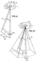
- Figures 9 and 10 illustrate certain hardware implementations for achieving the moving spread beam.
- both the x-ray source 10 and the detector assembly are translated along parallel linear paths indicated by arrows 100, 102 in Figure 9.
- Tests suggest that a preferable thickness for the spread beam is 8 millimeters at the input surface of the detector elements, but a beam from 1 to 50 millimeters in thickness can be used. This dimension is indicated by arrows 104 in Figure 9.
- the detector moves generally along an arcuate path indicated by arrows 108 in Figure 10.
- the source 10 can be pivoted about its x-ray focal spot to cause the x-ray beam to track the detector.
- the x-ray tube may be retained in a stationary disposition, the actual x-ray energy striking the detector being collimated by the collimating slit defining structures 16, 20, illustrated in Figures 9 and 10.
- the concept of this invention may be employed by maintaining the x-ray source and the detector both stationary, while the subject for examination moves along a linear path between the source and detector.
- Such an embodiment could be suitable, for example, in a baggage inspection system.
- a requirement peculiar to the system embodying this invention is that data is acquired in one x-ray spread beam scanning direction only. This direction is from left to right, as shown in Figure 1.
- the mechanical scanning apparatus should be capable of rapid retrace between production of sequential images. It is mechanically practicable to produce retrace at velocities much higher than scanning velocities.
- the detector itself should be coupled to the master scanning drive mechanism.
- the source, and the slit defining collimators should be the follower elements, since their instantaneous position is less critical than that of the detector.
- An encoder such as shown in Figure 1, coupled to the detector, provides timing pulses to control the position of the source and/or collimating slit defining structures.
- the pulses output from the encoder are also coupled to the clocking circuitry 56 to control the timing of charge stepping of the charge shifting and accumulating circuitry.
- Such an arrangement will assure good synchronization between detector motion in one direction and charge motion in the opposite direction at the same average velocity. Very accurate synchronization of charge and detector motion is possible since the moving charges on the detector ⁇ o not possess inertia and the charge shifting can be implemented with a favorable frequency response.
- Retrace and scanning rates, and hence frame repetition rate is substantially limited by only the mechanical considerations, not by optics or electronics. Tests have shown that frame repetition rates of about 30 per minute are feasible, using a frame size of 50 cm. X 50 cm.
- Figure 11 shows in more detail an embodiment of one of the imaging chips, indicated at reference character 150.
- the image chip comprises a 64 x 64 rectilinear array of individual detector elements, each comprising a photodiode.
- the detector elements are arranged in 64 rows and columns.
- one such row comprises individual detector elements Dl,l-Dl,64.
- Sixty-four rows of detector elements are present on the imaging chip, extending downwardly to the row comprising individual detector elements D64, 1-D64, 64.
- a shift register including cells 01-064 is coupled in parallel to the column of detector elements Dl,l-D64,1.
- the image chip, and the detector as a whole move to the right as indicated by the arrow in Figure 11.
- the shifting and integration circuitry cause accumulating charge motion in a direction to the left as shown in Figure 11, synchronously with the detector motion in the opposite direction.
- the charge packets are transferred in parallel to the shift register, i.e., into each of the cells 01-064.
- the data thus accumulated can be clocked out, digitized, and processed to yield image representations in a manner known in the art.
- the 64 x 64 array of individual detector elements of the image chip 150 of Figure 11 collectively describe a square of 8 millimeters length on a side.
- the detector 14 comprises a vertical column of such imaging chips, each being 8 millimeters wide, and the spread beam incident on the detector is vertically oriented and 8 millimeters in thickness, just sufficient to illuminate the entirety of the vertical column of imaging chips.
- Figure 12 illustrates another embodiment of an image chip indicated by the reference character 170.
- the image chip 170 comprises a 64 x 256 array of rectangular individual detector elements.
- the array comprises 64 horizontal rows of 256 elements each.
- Each individual element has a horizontal width which is approximately 1/4 its vertical height.
- the 64 x 256 detector array describes a square approximately 8 millimeters on a side.
- the detector during scanning, is moved to the right as shown in Figure 12, and the charge packets are shifted and integrated to the left, at a rate synchronous with that of detector motion.
- the embodiment of Figure 12 is considered particularly suitable for the use of time delay and integrate circuitry consisting of CC D elements.
- the 64 x 64 array of Figure 11 is considered more suitable for the use of bucket brigade circuitry which can handle wider charge "bins", and hence has a greater capability than CCD for shifting charge packets efficiently. Efficiencies of at least about 0.99995 are desirable.
- the charges are shifted to the left, as shown in Figure 11 in synchronism with detector scanning motion.
- Data respectively corresponding to projections of the same image line is integrated and transferred along each element until the charge reaches the extreme left-hand detector element in the leftmost column of detector elements, i.e. D1,1-D64,1.
- the charge packets are transferred and clocked successively through a series of parallel shift registers Sl-S8.
- the clocking through the registers Sl through S8 is at the same rate as the clocking along the various detector elements. No integration, however, takes place in the shift registers.
- circuitry of known type is provided which, in conjunction with the shift registers S1-S8, periodically sums output data in the shift registers Sl-S8. After each succession of four shifts, the data in S1-S4, corresponding to each separate element row, is separately summed in appropriate output register circuitry, and then clocked out to digitization circuitry and image processing circuitry such as described in connection with Figure 11.
- Figure 13 is a block diagram showing circuitry of the matrix array of an image chip in greater detail.
- the image chip shown comprises a 64 x 64 element bucket brigade matrix array for detecting x-rays after they have been converted to green light, similar to that of Figure 11.
- the matrix array is operated in a time delay integration mode.
- the center-to-center spacing of the individual detector elements in both the column and row directions is 5 mils.
- the array is integrated using a double poly-silicon gate NMOS process. The design details and dynamic range consideration of the image chip array are discussed in detail below.
- the image chip includes 64 horizontal bucket brigade (BBD) shift registers 201-264. Also included is a 128 element BBD shift register 265.
- BBD horizontal bucket brigade
- Each of the registers 201-265 is provided with a fat-zero input port (designated generally by reference characters 270, 272) for enhancing charge transfer efficiency in the registers.
- Registers 201-264 perform the time delay and integrate (TDI) function while register 265 transfers the signal charge package to an output sensing amplifier 274.
- the output sensing amplifier converts the charge to a signal voltage appearing at a lead 2 76 which is a function of the charge input to the amplifier.
- the signal at the lead 276 provides a video output.
- Each of the registers 2 01 - 264 comprises 64 BBD elements (32 stages) and is driven by a two-phase complementary clock having inputs designated by the reference characters 280, 282.
- Each BBD element is constructed with a diffused photodiode and a poly-silicon-to-poly-silicon storage capacitor.
- the sensing area of each photodiode is ap- proximately 50% of the total area of the individual detector element receiving surface.
- the capacitance of each individual detector element is about 1.2 picofarads (pF).
- the two-phase clocks at the leads 280, 282 shift the charge packages along each of the shift registers 201-264 toward the register 26 5.
- the clocking rates of the signals at the leads 280 , 282 is approximately 0.5 kilohertz (kHz).
- the total integration time of each pixel is approximately 64 milliseconds (msec).
- This relatively slow integration time allows a tolerance for x-ray tube rotor and voltage ripple, and substantially reduces their artifacts.
- the register 265 is driven by a two-phase clock having inputs 292, 294. This clock signal runs at a frequency 64 times faster than that of the clock signals at the leads 280, 282.
- the output sensing amplifier of the register 265 is a gated charge integrator which converts the signal charaes into output voltaqes.
- the clock waveforms 280, 282 and 292, 294 are complementary clocks, cross over at 50%.
- the rising edge of waveform 292 leads that of waveform 295 by about 30 nanoseconds (ns.) and waveform 295 leads waveform 280 by about 20 ns.
- the falling edge of waveform 295 leads that of waveform 292 by at least 30 ns.
- the charge handling capacity of the BBD elements depends upon the size of the storage capacitor and of the clock voltage. Assuming a maximum voltage swing of 5 volts at each BBD storage node, the saturation charge of each BBD element will be about 6 picocou lombs (pC), i.e., 1.2 pF x 5 v. This saturation charge is equivalent to a signal charge of 3.75 x 10 electrons.
- noise components there are two noise components in the signal output from the sensing amplifier.
- One is the fixed-pattern noise caused by nonuniformity of the input fat-zero among the registers 201-264. This noise component can be eliminated by external signal processing. Therefore it is not the limiting factor in the performance of the device.
- thermodynamic noise The other noise component is the thermodynamic noise.
- This noise consists of input kTc_noise, BBD transfer noise, dark current shot noise, photo signal shot noise and output amplifier noise.
- the dominant thermodynamic noise is BBD transfer noise.
- the noise electron charge due to this component, is approximately 6000 electrons. This noise figure results in a dynamic range of about 6250 (3.75 x 10 7 /10 3 ) for the device.
- Figures 15 and 16 illustrate other embodiments of a digital radiographic system utilizing time delay and integrate (TDI) techniques in scan projection radiography. These alternates possess an enhanced frame generation rate capability, and couple the use of area detectors with discrete element charge coupled imagers-operating in the TDI mode.
- TDI time delay and integrate
- x-rays from a source (not shown) and defined by ray lines 300 are directed toward a subject 302.
- the x-rays are directed generally toward an approximately cylindrical image intensifier tube 312, and more particularly toward an input face 313 of the image tube.
- the x-ray pattern incident upon the image tube causes the image tube to respond by generating a corresponding smaller, relatively bright visible light pattern at an output face 314.
- a slit collimator 304 is interposed between the source and the subject.
- the slit collimator is made of a material which is substantially impervious to x-rays, and in which is defined a plurality of slits such as indicated by reference character 306.
- the slit collimator is mounted for movement transverse to the incident x-rays in the directions indicated by the arrow set 308 in Figure 15.
- a servo mechanism 305 is coupled to the slit collimator 304 to effect this movement in a fashion described in more detail below.
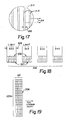
- the incidence of the x-ray slit patterns causes the image tube 312 to produce a plurality of visible light slit patterns 315 (see Figure 17) at the output face 314 .
- One such light slit pattern is produced corresponding to each x-ray slit pattern falling upon the input face 314.
- the light slit patterns appearing at the output face 314 lie along respective axes which are perpendicular to the paper with respect to Figure 15.
- the light patterns have a width designated by reference character 329 ( Figures 17 and 16).
- Each of the slit light patterns appearing at the output face 314 is projected through a collimating lens 318 and onto the surface of a partially transmissive mirror 320.
- the mirror 320 is a plane mirror extending perpendicular to the paper as viewed in Figure 15.
- the mirror 320 is oriented at approximately 45° with respect to the central axis of the image intensifier tube 312.
- each of the slit light patterns strikes the mirror 320 at a slightly different location along its surface.
- the slit light patterns are projected horizontally as shown in Figure 15 onto.a second planar mirror 322.
- the mirror 322 is mounted pivotally with respect to an axis 323 extending perpendicular with respect to the paper as shown in Figure 15.
- the slit light patterns are reflected from the mirror 322 through a second collimating lens 324 and optionally through other optical elements, not shown -r. but suitably provided by one of skill in the art, onto a detector assembly 325 comprising a set of detector arrays 326.
- the detector arrays 326 are stationary with respect to the image intensifier tube 312, and with respect to the mirror 320.
- the detector arrays 326 are equal in number to the number of slit light patterns projected toward the detector 325. See Figure 18 for detail.
- Each of the detector arrays 326 suitably comprises a separate rectangular array of small individual detector elements.
- the rectangular configuration of each array is elongated along an axis perpendicular to the paper in Figure 15. More specifically, tests have shown that a suitable embodiment for each of the detector arrays 326 comprises either a 1024 X 64 or 2048 X 64 array of individual detector elements (see, e.g., Figure 19).
- Each of the detector arrays 326 is constructed analogously to the detector array embodiments described in simplified form in connection with Figure 5 and in more detail in connection with Figures 13 and 14.
- each detector array 326 Coupled to each detector array 326 is a system 327 of time delay and integrate circuitry. This circuitry and its operation is analogous to that discussed above in connection with Figures 4A-4D, 5, 13 and 14.
- a pivot apparatus 330 is coupled to the pivotable mirror 322. In response to a command signal from the operator's console, the pivot apparatus 330 operates to pivot the mirror 322 in a manner described in more detail below.
- the pivot apparatus 330 is coupled to an encoder 332.
- the encoder 332 senses the rotational position of the mirror 322, as determined by the pivot apparatus 330, and produces a signal at a lead 334 representing substantially the instantaneous rotational orientation of the mirror 322.
- the signal at the lead 334 is transmitted to the servo mechanism 305 in order to synchronize the translational movement of the slit col- l i m ator 304 along the path indicated by the arrows 308 The nature of this synchronization is described more fully below.
- Another output from the encoder 332 is transmitted over a lead 336 to the time delay and integrate circuitry 327 associated with each detector array 326.
- the signal at the lead 336 from the encoder 332 synchronizes the clocking circuitry of the time delay and integrate ci r - cu itry in order to synchronize the charge shifting func - t io n with the angular velocity of the pivotable mirror 322 and the translational velocity of the slit collimator 304.
- the encoder 332 can suitably comprise any of a plurality of known types of such devices, for example, the encoder apparatus and circuitry described in the above incorporated United States Letters Patent to Manring.
- the pivoting motion of the mirror 322 and the translational motion of the slit collimator 304 are synchronously coordinated in order to maintain the projection of each of the slit light patterns propo- gated from the output face 314 stationary with respect to the detector assembly 325, notwithstanding the motion of the slit light patterns across the output face 314.
- a motion of the slit collimator from left to right must be accompanied by a corresponding pivoting of the mirror 322 in a clockwise direction.
- the ratio of the translational velocity of the slit collimator 304 to the angular velocity of pivoting of the mirror 322 in order to maintain the stationary projection of each of the slit light patterns on the detector 325 is determined by the particular geometry and optics of the system, and can readily be determined by one of ordinary skill given the above system design parameters.
- the translation of the slit collimator may be over the whole width of the input face, depending, as illustrated for example below, on the system configuration.
- signals from the encoder 332 are utilized to clock the time delay and integrate circuitry 327 associated with each of the detector arrays 326.
- the direction and average clocking velocity of the charge packets produced by the elements 326 is a function of both the velocity and direction of translation of the slit collimator 304 during scanning.
- the charge shifting is in a direction opposite in sense to the direction of movement of the slit light patterns across the output face 314 of the image tube. More specifically, if scanning is conducted with the system of Figure 15 and with the slit collimator 304 moving in a direction from left to right, the direction of clocking of the charge shifting motion is to be in a right to left direction as illustrated with respect to the detector 325.
- each of the slits of the collimator 304 is chosen such that the projections 329 (see Figure 18) of the slit light patterns are each of a width equal to that_of one of the detector arrays 326.
- the average velocity of the clocking of charge shifting motion is, under these conditions, chosen to be a velocity such that charge is shifted across the entirety of the width of one of the detector elements 326 in the same amount of time which is required for a slit light pattern appearing at the image tube output face 314 to traverse a distance equal to its own width.
- the partially transmissive mirror 320 comprises a form of beamsplitter.
- the portion of light energy from the output face 314 which is transmitted through the mirror 320, is prop- goated through a lens 339 and onto the input 340 of a video system.
- the video system can comprise any of a number of such systems known in the art as suitable for use in fluorography applications where an image intensifier tube is employed. Accordingly, the remainder of the video system is not illustrated.
- the system of Figure 15 can be operated as a conventional bright fluoroscopic system, Conversely, a conventional fluoroscopic system can be converted to add digital radiographic capabilities such as described above by adding the movable slit collimator 304 , pivotable mirror 322, detector assembly 32 5 , and their associated mechanical and electronic synchronization equipment as shown and described in connection with Figure 15.
- Figure 16 illustrates another embodiment, similar. but not identical, to that of Figure 15.
- the detector and lens arrangement could be reoriented to directly view the light pattern from the partially transmissive mirror, and that mirror could be arranged to pivot. In such a case, the second mirror could be omitted.
- x-rays are directed toward a slit collimator 352.
- the slit collimator defines a single slit 353 having its longitudinal dimension extending perpendicular to the paper as shown in Figure 16.
- X-rays passing through the slit 353 are directed through a subject 356 and onto an input face 360 of an image intensifier tube 358.
- the single slit x-ray pattern falling on the input face 360 causes the intensifier tube to generate at an output face 359 a single slit light image representing the x-rays of the slit pattern falling upon the input face.
- An image of the slit light pattern is projected through a collimating lens arrangement 361 and onto a beam splitter comprising a partially transmissive mirror 362.
- the mirror 362 has a planar configuration similar to the mirror 320 in Figure 15.
- the image of the single slit light pattern is projected onto a second planar mirror 364 which is pivotally mounted about an axis 366.
- the image reflected from the mirror 364 is projected through a lensing arrangement 370 and onto the input of a detector 371.
- the detector 371 comprises a single rectangular pattern of individual solid state discrete detector elements, arranged in an elongated pattern similar in configuration to that shown in Figure 19.
- the rectangular element array can suitably comprise a 64 X 1024 or a 64 X 2048 array of elements.
- the width of the detector array 372 is approximately 8 millimeters.
- Time delay and integrate circuitry 374 is coupled to the respective transverse rows of individual detector elements of the array 372.
- the detector elements of the array 372 and the time delay and integrate circuitry 374 are analogous in structure and operation to that described in connection with Figure 15.
- FIG. 16 An important difference between the embodiments of Figures 15 and 16 is that the embodiment of Figure 16 uses a slit collimator having only a single slit, and produces at the output face 359 a single slit light pattern. Since only one slit light pattern is generated, only the one array of individual detector elements 372 is required for the detector 371.
- the pivotally mounted mirror 364 is coupled to a pivot apparatus 389 which serves to controllably pivot the mirror about its axis 366.
- the pivot apparatus 389 is responsive to a command signal from the operator's console to so pivot the mirror.
- An output from the pivot apparatus 389 is coupled to an encoder 390 which produces a signal indicating substantially the instantaneous angular displacement of the mirror 364 about its axis 366 .
- An output of the encoder 390 is directed to a servo apparatus 392.
- the servo apparatus 392 is coupled to the slit collimator 352 in order to move the slit collimator to the right and left, as commanded, and as illustrated by the directions indicated by the arrows 354.
- the encoder 390 produces another output on a lead 393 which is directed to the time delay and integrate circuitry 374 of the detector 371.
- the circuitry and functioning of the encoder with respect to the time delay and integrate circuitry 374 is analogous to that described in connection with Figure 15. That is, the signal from the encoder clocks the time delay and integrate circuitry to shift the charges generated by the individual detector elements in a direction opposite in sense to the direction of movement of the slit light pattern across the output face 359.
- the second mirror of Figure 16 can be omitted in a manner analogous to that described in connection with the Figure 15 embodiment.
- Figures 15 and 16 are feasable for operation without slit collimators interposed downstream of the image tube output face. However, scatter rejection can be further improved if an appropriate slit collimator were employed just ahead of the discrete solid state detector.
- the longitudinal dimensions of the individual arrays of discrete solid state detector arrays are designed to be sufficiently tall to accommodate the full length of a slit light pattern appearing at the output face of the intensifier tube.
- optics associated only with the branch of the system directed toward the TDI detectors can correct for pin cushion distortion and can also control the amount of light incident on the solid state detector, independently of influencing light directed toward the video portion of the system.
- the output of the solid state detector can be transmitted directly to a digital camera to provide a hard copy. Accordingly, the system of Figures 15 and 16 can be employed to do fluoroscopic examinations utilizing the video branch of the system, while still having capability of providing high quality digital scans utilizing the discrete solid state detector portion.
Landscapes
- Health & Medical Sciences (AREA)
- Life Sciences & Earth Sciences (AREA)
- Physics & Mathematics (AREA)
- High Energy & Nuclear Physics (AREA)
- Molecular Biology (AREA)
- Medical Informatics (AREA)
- General Physics & Mathematics (AREA)
- Spectroscopy & Molecular Physics (AREA)
- Engineering & Computer Science (AREA)
- General Health & Medical Sciences (AREA)
- Biomedical Technology (AREA)
- Optics & Photonics (AREA)
- Nuclear Medicine, Radiotherapy & Molecular Imaging (AREA)
- Surgery (AREA)
- Radiology & Medical Imaging (AREA)
- Heart & Thoracic Surgery (AREA)
- Pathology (AREA)
- Animal Behavior & Ethology (AREA)
- Biophysics (AREA)
- Public Health (AREA)
- Veterinary Medicine (AREA)
- Apparatus For Radiation Diagnosis (AREA)
- Analysing Materials By The Use Of Radiation (AREA)
- Transforming Light Signals Into Electric Signals (AREA)
- Radiography Using Non-Light Waves (AREA)
Applications Claiming Priority (2)
| Application Number | Priority Date | Filing Date | Title |
|---|---|---|---|
| US62288884A | 1984-06-21 | 1984-06-21 | |
| US622888 | 1984-06-21 |
Publications (2)
| Publication Number | Publication Date |
|---|---|
| EP0166567A2 true EP0166567A2 (de) | 1986-01-02 |
| EP0166567A3 EP0166567A3 (de) | 1986-11-26 |
Family
ID=24495915
Family Applications (1)
| Application Number | Title | Priority Date | Filing Date |
|---|---|---|---|
| EP85304356A Withdrawn EP0166567A3 (de) | 1984-06-21 | 1985-06-18 | Vorrichtung und Verfahren zur Bilderzeugung |
Country Status (2)
| Country | Link |
|---|---|
| EP (1) | EP0166567A3 (de) |
| JP (1) | JPS6122841A (de) |
Cited By (14)
| Publication number | Priority date | Publication date | Assignee | Title |
|---|---|---|---|---|
| DE4200653A1 (de) * | 1992-01-13 | 1993-07-15 | Siemens Ag | Roentgenaufnahmegeraet fuer roentgenschattenbilder |
| EP0632995A1 (de) * | 1993-07-06 | 1995-01-11 | Siemens Aktiengesellschaft | Zahnärztliche Röntgendiagnostikeinrichtung |
| EP0632994A1 (de) * | 1993-07-06 | 1995-01-11 | Siemens Aktiengesellschaft | Röntgendiagnostikeinrichtung zur Erstellung von Röntgenaufnahmen von Körperteilen eines Patienten |
| EP0634671A1 (de) * | 1993-07-06 | 1995-01-18 | Siemens Aktiengesellschaft | Zeilendetektor-Kamera für die Verwendung bei insbesondere zahnärztlichen Röntgendiagnostikgeräten |
| FR2755815A1 (fr) * | 1996-11-08 | 1998-05-15 | Commissariat Energie Atomique | Dispositif et procede de determination de la position presumee d'un evenement par rapport a un ensemble de photodetecteurs, et application aux gamma-cameras |
| EP0988777A4 (de) * | 1997-05-20 | 2004-07-07 | Fischer Imaging Corp | Digitales abstatgerät für mammographie unter verwendung einer selbstanpassenolengeschwindigkeitsrückführung und verfahren dazu |
| DE102008007595A1 (de) * | 2008-02-06 | 2009-08-13 | Fraunhofer-Gesellschaft zur Förderung der angewandten Forschung e.V. | Vorrichtung und Verfahren zum Erfassen eines Bildes |
| WO2009098014A3 (de) * | 2008-02-06 | 2010-02-25 | Fraunhofer-Gesellschaft zur Förderung der angewandten Forschung e.V. | Vorrichtung und verfahren zum erfassen eines bildes |
| US7772561B2 (en) | 2008-02-06 | 2010-08-10 | Fraunhofer-Gesellschaft Zur Foerderung Der Angewandten Forschung E.V. | Apparatus and method for detecting an image |
| EP2251680A3 (de) * | 2009-05-13 | 2012-02-08 | Ishida Co., Ltd. | Röntgenstrahlinspektionsvorrichtung |
| US10539517B2 (en) | 2017-09-08 | 2020-01-21 | Sumitomo Chemical Company, Limited | Checking device and checking method |
| US10551329B2 (en) | 2017-09-08 | 2020-02-04 | Sumitomo Chemical Company, Limted | Checking device |
| EP3648453A1 (de) * | 2018-10-31 | 2020-05-06 | Uniwersytet Warszawski | System zur detektion mit hoher zeitlicher und räumlicher auflösung und verfahren zur detektion mit hoher zeitlicher und räumlicher auflösung |
| CN115406916A (zh) * | 2022-11-02 | 2022-11-29 | 北京紫方启研科技有限公司 | 实现大面积检测的分体式x射线检测系统及其方法 |
Families Citing this family (10)
| Publication number | Priority date | Publication date | Assignee | Title |
|---|---|---|---|---|
| US4878234A (en) * | 1987-02-16 | 1989-10-31 | Siemens Aktiengesellschaft | Dental x-ray diagnostics installation for producing panorama slice exposures of the jaw of a patient |
| JPH01241536A (ja) * | 1988-03-23 | 1989-09-26 | Hitachi Ltd | X線画像検出装置 |
| GB9121789D0 (en) * | 1991-10-14 | 1991-11-27 | Minnesota Mining & Mfg | Positive-acting photothermographic materials |
| JP3291406B2 (ja) * | 1995-02-09 | 2002-06-10 | 株式会社モリタ製作所 | パノラマx線撮影装置 |
| JP3319905B2 (ja) * | 1995-03-24 | 2002-09-03 | 株式会社モリタ製作所 | デジタルx線撮影装置 |
| JP3307519B2 (ja) * | 1995-03-24 | 2002-07-24 | 株式会社モリタ製作所 | 医療用x線撮影装置 |
| FI119173B (fi) * | 2001-11-23 | 2008-08-29 | Planmed Oy | Anturijärjestely ja menetelmä digitaalisessa pyyhkäisykuvantamisessa |
| WO2011145171A1 (ja) | 2010-05-18 | 2011-11-24 | キヤノン株式会社 | 撮像システム及びその制御方法 |
| JP7138515B2 (ja) | 2017-09-08 | 2022-09-16 | 住友化学株式会社 | 検査装置 |
| JP7175675B2 (ja) | 2017-09-08 | 2022-11-21 | 住友化学株式会社 | 検査装置および検査方法 |
Family Cites Families (6)
| Publication number | Priority date | Publication date | Assignee | Title |
|---|---|---|---|---|
| US4144457A (en) * | 1976-04-05 | 1979-03-13 | Albert Richard D | Tomographic X-ray scanning system |
| DE3028085A1 (de) * | 1980-07-24 | 1982-02-25 | Siemens AG, 1000 Berlin und 8000 München | Roentgendiagnostikeinrichtung fuer indirekt-aufnahmen |
| DE3037621A1 (de) * | 1980-10-04 | 1982-05-27 | Philips Patentverwaltung Gmbh, 2000 Hamburg | Durchleuchtungsanordnung zur aufnahme von schichtbildern eines dreidimensionalen objektes |
| DE3104052A1 (de) * | 1981-02-06 | 1982-08-19 | Philips Patentverwaltung Gmbh, 2000 Hamburg | "roentgenuntersuchungsanordnung mit hoher ortsaufloesung" |
| NL8101667A (nl) * | 1981-04-03 | 1982-11-01 | Philips Nv | Stralingsonderzoekapparaat met filmgeheugen. |
| DE3134076A1 (de) * | 1981-08-28 | 1983-03-10 | Philips Patentverwaltung Gmbh, 2000 Hamburg | "vorrichtung zur schichtweisen darstellung eines koerpers" |
-
1985
- 1985-06-18 EP EP85304356A patent/EP0166567A3/de not_active Withdrawn
- 1985-06-21 JP JP60136746A patent/JPS6122841A/ja active Pending
Cited By (21)
| Publication number | Priority date | Publication date | Assignee | Title |
|---|---|---|---|---|
| DE4200653A1 (de) * | 1992-01-13 | 1993-07-15 | Siemens Ag | Roentgenaufnahmegeraet fuer roentgenschattenbilder |
| US5293416A (en) * | 1992-01-13 | 1994-03-08 | Siemens Aktiengesellschaft | Radiography apparatus for producing X-ray shadowgraphs |
| EP0632995A1 (de) * | 1993-07-06 | 1995-01-11 | Siemens Aktiengesellschaft | Zahnärztliche Röntgendiagnostikeinrichtung |
| EP0632994A1 (de) * | 1993-07-06 | 1995-01-11 | Siemens Aktiengesellschaft | Röntgendiagnostikeinrichtung zur Erstellung von Röntgenaufnahmen von Körperteilen eines Patienten |
| EP0634671A1 (de) * | 1993-07-06 | 1995-01-18 | Siemens Aktiengesellschaft | Zeilendetektor-Kamera für die Verwendung bei insbesondere zahnärztlichen Röntgendiagnostikgeräten |
| US5511106A (en) * | 1993-07-06 | 1996-04-23 | Siemens Aktiengesellschaft | X-ray diagnostics installation for producing x-ray exposures of body parts of a patient |
| US5579366A (en) * | 1993-07-06 | 1996-11-26 | Siemens Aktiengesellschaft | Line detector camera for employment in, particularly, dental x-ray diagnostics installations |
| FR2755815A1 (fr) * | 1996-11-08 | 1998-05-15 | Commissariat Energie Atomique | Dispositif et procede de determination de la position presumee d'un evenement par rapport a un ensemble de photodetecteurs, et application aux gamma-cameras |
| WO1998021607A1 (fr) * | 1996-11-08 | 1998-05-22 | Commissariat A L'energie Atomique | Dispositif et procede de determination de la position presumee d'un evenement par rapport a un ensemble de photodetecteurs, et application aux gamma-c |
| EP0988777A4 (de) * | 1997-05-20 | 2004-07-07 | Fischer Imaging Corp | Digitales abstatgerät für mammographie unter verwendung einer selbstanpassenolengeschwindigkeitsrückführung und verfahren dazu |
| DE102008007595A1 (de) * | 2008-02-06 | 2009-08-13 | Fraunhofer-Gesellschaft zur Förderung der angewandten Forschung e.V. | Vorrichtung und Verfahren zum Erfassen eines Bildes |
| WO2009098014A3 (de) * | 2008-02-06 | 2010-02-25 | Fraunhofer-Gesellschaft zur Förderung der angewandten Forschung e.V. | Vorrichtung und verfahren zum erfassen eines bildes |
| US7772561B2 (en) | 2008-02-06 | 2010-08-10 | Fraunhofer-Gesellschaft Zur Foerderung Der Angewandten Forschung E.V. | Apparatus and method for detecting an image |
| US7807975B2 (en) | 2008-02-06 | 2010-10-05 | Fraunhofer-Gesellschaft Zur Foerderung Der Angewandten Forschung E.V. | Apparatus and method for detecting an image |
| CN101939667B (zh) * | 2008-02-06 | 2013-03-20 | 弗劳恩霍夫应用研究促进协会 | 用于检测图像的设备和方法 |
| DE102008007595B4 (de) | 2008-02-06 | 2018-04-05 | Fraunhofer-Gesellschaft zur Förderung der angewandten Forschung e.V. | Vorrichtung und Verfahren zum Erfassen eines Bildes |
| EP2251680A3 (de) * | 2009-05-13 | 2012-02-08 | Ishida Co., Ltd. | Röntgenstrahlinspektionsvorrichtung |
| US10539517B2 (en) | 2017-09-08 | 2020-01-21 | Sumitomo Chemical Company, Limited | Checking device and checking method |
| US10551329B2 (en) | 2017-09-08 | 2020-02-04 | Sumitomo Chemical Company, Limted | Checking device |
| EP3648453A1 (de) * | 2018-10-31 | 2020-05-06 | Uniwersytet Warszawski | System zur detektion mit hoher zeitlicher und räumlicher auflösung und verfahren zur detektion mit hoher zeitlicher und räumlicher auflösung |
| CN115406916A (zh) * | 2022-11-02 | 2022-11-29 | 北京紫方启研科技有限公司 | 实现大面积检测的分体式x射线检测系统及其方法 |
Also Published As
| Publication number | Publication date |
|---|---|
| EP0166567A3 (de) | 1986-11-26 |
| JPS6122841A (ja) | 1986-01-31 |
Similar Documents
| Publication | Publication Date | Title |
|---|---|---|
| EP0166567A2 (de) | Vorrichtung und Verfahren zur Bilderzeugung | |
| US4817123A (en) | Digital radiography detector resolution improvement | |
| US4389729A (en) | High resolution digital radiography system | |
| US5138642A (en) | Detector imaging arrangement for an industrial CT device | |
| US4878234A (en) | Dental x-ray diagnostics installation for producing panorama slice exposures of the jaw of a patient | |
| EP0061496B1 (de) | Detektor-system mit bildverstärker für elektronische röntgenaufnahmen | |
| US4179100A (en) | Radiography apparatus | |
| US4383327A (en) | Radiographic systems employing multi-linear arrays of electronic radiation detectors | |
| US4511799A (en) | Dual energy imaging | |
| US6895080B2 (en) | X-ray measuring apparatus | |
| US4352986A (en) | Tomographic apparatus for the production of transverse layer images | |
| EP0051350B1 (de) | Abtastblende zur Darstellung einer Absorptionsverteilung mittels eines Sichtgerätes | |
| US5018177A (en) | Apparatus and method for producing digital panoramic x-ray images | |
| JPH0661324B2 (ja) | 放射線撮影装置 | |
| USRE32164E (en) | Radiographic systems employing multi-linear arrays of electronic radiation detectors | |
| KR20110004839A (ko) | 의료용 x선 촬상 시스템 | |
| KR20110008002A (ko) | 의료용 x선 촬상 시스템 | |
| US4164657A (en) | Apparatus for tomography | |
| CN108414541A (zh) | X射线透视检查装置 | |
| EP0138625A2 (de) | Röntgengerät | |
| EP0140695A2 (de) | Digitaler Röntgenaufnahmeapparat | |
| JPH06237927A (ja) | 放射線画像撮影装置 | |
| USRE32779E (en) | Radiographic systems employing multi-linear arrays of electronic radiation detectors | |
| EP0263210B1 (de) | Röntgenbildaufnahmegerät mit hohem Kontrast | |
| EP0049464B1 (de) | Gerät zum Erfassen von Röntgenstrahl-Absorptionswerten mittels eines rechnergesteuerten Tomographie-Gerätes |
Legal Events
| Date | Code | Title | Description |
|---|---|---|---|
| PUAI | Public reference made under article 153(3) epc to a published international application that has entered the european phase |
Free format text: ORIGINAL CODE: 0009012 |
|
| AK | Designated contracting states |
Designated state(s): DE FR GB NL |
|
| PUAL | Search report despatched |
Free format text: ORIGINAL CODE: 0009013 |
|
| AK | Designated contracting states |
Kind code of ref document: A3 Designated state(s): DE FR GB NL |
|
| STAA | Information on the status of an ep patent application or granted ep patent |
Free format text: STATUS: THE APPLICATION IS DEEMED TO BE WITHDRAWN |
|
| 18D | Application deemed to be withdrawn |
Effective date: 19870527 |
|
| RIN1 | Information on inventor provided before grant (corrected) |
Inventor name: TESIC, MICHAEL M. Inventor name: DEMEESTER, GORDON D. Inventor name: MATTSON, RODNEY A. |