EP0167157B1 - Circuit de retard - Google Patents
Circuit de retard Download PDFInfo
- Publication number
- EP0167157B1 EP0167157B1 EP19850108223 EP85108223A EP0167157B1 EP 0167157 B1 EP0167157 B1 EP 0167157B1 EP 19850108223 EP19850108223 EP 19850108223 EP 85108223 A EP85108223 A EP 85108223A EP 0167157 B1 EP0167157 B1 EP 0167157B1
- Authority
- EP
- European Patent Office
- Prior art keywords
- delay
- node
- coupled
- signal
- inverter
- Prior art date
- Legal status (The legal status is an assumption and is not a legal conclusion. Google has not performed a legal analysis and makes no representation as to the accuracy of the status listed.)
- Expired
Links
- 230000003111 delayed effect Effects 0.000 claims description 19
- 238000002604 ultrasonography Methods 0.000 claims description 14
- 230000008878 coupling Effects 0.000 claims description 9
- 238000010168 coupling process Methods 0.000 claims description 9
- 238000005859 coupling reaction Methods 0.000 claims description 9
- 238000009738 saturating Methods 0.000 claims description 9
- 230000005669 field effect Effects 0.000 claims description 5
- 238000012285 ultrasound imaging Methods 0.000 claims description 3
- 230000002463 transducing effect Effects 0.000 claims 4
- 238000010586 diagram Methods 0.000 description 29
- 230000010363 phase shift Effects 0.000 description 12
- 230000001934 delay Effects 0.000 description 11
- 238000013461 design Methods 0.000 description 11
- 230000003247 decreasing effect Effects 0.000 description 7
- 238000003384 imaging method Methods 0.000 description 7
- 238000000034 method Methods 0.000 description 7
- 230000035945 sensitivity Effects 0.000 description 5
- 230000007423 decrease Effects 0.000 description 4
- 210000000056 organ Anatomy 0.000 description 4
- 230000000644 propagated effect Effects 0.000 description 3
- 230000000630 rising effect Effects 0.000 description 3
- 230000000694 effects Effects 0.000 description 2
- 230000010354 integration Effects 0.000 description 2
- 238000010276 construction Methods 0.000 description 1
- 238000012937 correction Methods 0.000 description 1
- 230000001419 dependent effect Effects 0.000 description 1
- 238000011161 development Methods 0.000 description 1
- 230000018109 developmental process Effects 0.000 description 1
- 230000007613 environmental effect Effects 0.000 description 1
- 230000010355 oscillation Effects 0.000 description 1
- 238000010615 ring circuit Methods 0.000 description 1
- 238000005070 sampling Methods 0.000 description 1
- 229910052710 silicon Inorganic materials 0.000 description 1
- 239000010703 silicon Substances 0.000 description 1
- 230000001360 synchronised effect Effects 0.000 description 1
- 238000012546 transfer Methods 0.000 description 1
Images








Classifications
-
- G—PHYSICS
- G01—MEASURING; TESTING
- G01S—RADIO DIRECTION-FINDING; RADIO NAVIGATION; DETERMINING DISTANCE OR VELOCITY BY USE OF RADIO WAVES; LOCATING OR PRESENCE-DETECTING BY USE OF THE REFLECTION OR RERADIATION OF RADIO WAVES; ANALOGOUS ARRANGEMENTS USING OTHER WAVES
- G01S7/00—Details of systems according to groups G01S13/00, G01S15/00, G01S17/00
- G01S7/52—Details of systems according to groups G01S13/00, G01S15/00, G01S17/00 of systems according to group G01S15/00
- G01S7/52017—Details of systems according to groups G01S13/00, G01S15/00, G01S17/00 of systems according to group G01S15/00 particularly adapted to short-range imaging
- G01S7/52046—Techniques for image enhancement involving transmitter or receiver
-
- H—ELECTRICITY
- H03—ELECTRONIC CIRCUITRY
- H03H—IMPEDANCE NETWORKS, e.g. RESONANT CIRCUITS; RESONATORS
- H03H11/00—Networks using active elements
- H03H11/02—Multiple-port networks
- H03H11/26—Time-delay networks
-
- H—ELECTRICITY
- H03—ELECTRONIC CIRCUITRY
- H03K—PULSE TECHNIQUE
- H03K5/00—Manipulating of pulses not covered by one of the other main groups of this subclass
- H03K5/13—Arrangements having a single output and transforming input signals into pulses delivered at desired time intervals
- H03K5/131—Digitally controlled
-
- H—ELECTRICITY
- H03—ELECTRONIC CIRCUITRY
- H03K—PULSE TECHNIQUE
- H03K7/00—Modulating pulses with a continuously-variable modulating signal
- H03K7/06—Frequency or rate modulation, i.e. PFM or PRM
-
- H—ELECTRICITY
- H03—ELECTRONIC CIRCUITRY
- H03K—PULSE TECHNIQUE
- H03K7/00—Modulating pulses with a continuously-variable modulating signal
- H03K7/08—Duration or width modulation ; Duty cycle modulation
-
- H—ELECTRICITY
- H03—ELECTRONIC CIRCUITRY
- H03K—PULSE TECHNIQUE
- H03K5/00—Manipulating of pulses not covered by one of the other main groups of this subclass
- H03K2005/00013—Delay, i.e. output pulse is delayed after input pulse and pulse length of output pulse is dependent on pulse length of input pulse
- H03K2005/0015—Layout of the delay element
- H03K2005/00195—Layout of the delay element using FET's
Definitions
- the invention relates to a delay circuit according to the preamble of claim 1.
- Such a delay circuit is known from US-A-4 099 204.
- a delay circuit of another kind is known from US-A-3 760 280.
- an analog input signal is converted into a frequency modulated (FM) signal which in turn is delayed by means of a clocked digital shift register.
- the delayed signal is then demodulated to provide a delayed analog output signal.
- FM frequency modulated
- the known delay circuit has the disadvantage that it reduces the bandwidth of the analog signal to be delayed.
- the bandwidth could theoretically be increased by increasing the clock frequency of the shift register, the bandwidth is limited in that for higher clock frequencies the expenditure of circuitry becomes very high and in that undesired high-frequency spurious emissions occur.
- the shift register would have to be clocked with a frequency at or above 10 GHz, thus causing disturbing high-frequency emissions.
- the delay circuit known from the US-A-4 099 204 comprises a fixed number of inverter stages, each delaying a FM-modulated input signal by an incremental delay amount. Taps are provided at each incremental delay stage, wherein a tap control logic controls a switching circuit for deriving from the delay circuit a delayed output signal having a variable delay which is determined by the tap control logic.
- the delayed time of the known delay circuit can be adjusted by varying the supply voltage; the known delay circuit includes a sync separator which separates a certain synchronisation sequence from the delayed pulses and an error detector which compares the separated synchronisation sequence with a reference synchronisation signal. An error signal which results from the comparison is used for adjustment of the delay amount of the delay circuit.
- the EP-A-0 059 802 describes a further known delay circuit for delaying pulses which are derived from horizontal synchronising pulses of a colour television set.
- the delay circuit comprises cascaded inverter stages, each of which includes a field effect transistor for providing a resistance to current flow and field effect transfer transistors.
- an odd number of stages of the inverted chain are coupled into a ring counter circuit which thereby creates a self-oscillation, the frequency of which is depending on the delay time of each inverter.
- By means of counting the frequency of the self-oscillation signal it is possible to determine the actual delay time, whereby the adjustable resistance elements are adjusted so, that the actual delay time is matching with a reference delay time.
- the known delay circuit has disadvantageous effects in that the adjustment operation cannot be carried out during the normal operating time, because the delay circuit must be switched into the ring counter configuration which is carried out during the fly-back period of the television apparatus. Furtheron, as the primary condition for generating self-oscillation, a certain odd number of inverter stages has to be coupled together into the ring circuit, thereby leaving at least one delay circuit which cannot be adjusted. Furtheron, for the adjustment of the delay time of the known delay circuit a very precise clock frequency has to be generated and applied to the frequency counters.
- each inverter stage of the delay circuit has a simple circuit construction and allows a continuous adjustment during the normal operation of the delay circuit by comparison of the phase of the input signal to the delay circuit with the phase of its output signal.
- the dependent claims 2 to 10 specify advantageous developments thereof.
- Claims 11 to 14 specify the use of the delay circuit in an ultrasound imaging system.
- the invention permits the design of the circuit which delays a plurality of analog input signals by adjustable different delay times and derives an output signal corresponding to the sum of the delayed signals.
- the invention allows to sum up pulse width modulated signals prior to being supplied to a demodulator and to supply the sum signal to a common demodulator, so that it is not necessary to have a demodulator for each individual delay circuit.
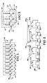
- Figure 1 is a schematic diagram of cascaded inverters used in an embodiment of the present invention.
- Figure 2 shows a circuit which uses a switch to vary propagation time through the circuit.
- Figure 3 shows a circuit which varies propagation delay from an input to an output by means of switches organized in the form of a binary tree.
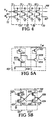
- Figure 4 shows a circuit which varies propagation delay by means of an analog signal.
- Figures 5A - 5B show the coupling of two inverters to form a delay stage.
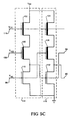
- Figures 5C - 5E show the coupling of two inverters to form a delay stage used in an embodiment of the present invention.
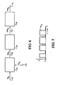
- Figure 6 is a block diagram of an analog signal delay circuit in accordance with a preferred embodiment of the present invention.
- Figure 7 shows a typical waveform of a signal at a location on the circuit of Figure 6.
- Figure 8 is a block diagram of an analog signal delay circuit utilizing pulse width modulation.
- Figures 8A - 8C show alternative designs for pulse width modulators which may be used with the analog signal delay circuit shown in Figure 8.
- Figure 8D shows a timing diagram for voltage signals in comparators shown in Figures 8A - 8C.
- Figure 9A shows another design for a pulse width modulator.
- Figure 9B is a timing diagram of signals from the pulse width modulator shown in Figure 9A.
- Figure 9C shows an alternative design for a pulse width modulator.
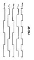
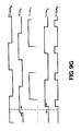
- Figures 9D - 9G are timing diagrams of signals from the pulse width modulator shown in Figure 9C.
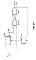
- Figure 10 is a block diagram of an analog signal delay circuit utilizing frequency modulation.
- Figure 11 is a block diagram of an analog signal delay circuit utilizing phase modulation.
- Figure 12 shows a block diagram of a circuit which may be used for either frequency modulation or phase modulation.
- Figures 13A and 13B are block diagrams of a transversal filter using the delay element according to the invention.
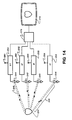
- Figure 14 is a block diagram of an acoustic imaging system using the delay circuit according to an embodiment of the invention.
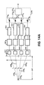
- Figure 14A - 14B shows details of delay architecture for the acoustic imaging system of Figure 14.
- Figure 15 is a block diagram of an FM detector utilizing the delay element according to an embodiment of the invention.
- Figure 15A is a graph showing how an increase in time delay increases the sensitivity of the detector shown in Figure 15.
- Figure 16 is a block diagram of an apparatus for calibrating delay time through a delay circuit.
- Figure 17 shows a more detailed block diagram of the apparatus of Figure 16 adapted for integration into delay architecture for the acoustic imaging system of Figure 14.
- Figure 18 shows an alternative embodiment of a calibration apparatus utilizing a ring oscillator.
- Delay of a binary signal may be accomplished by coupling the signal through a series of saturating elements. What is meant by a binary signal is a signal which changes between two voltage levels.
- the voltage levels, commonly referred to as logic 0 and logic 1 may be, for example, 0 volts and 3 volts.
- a binary signal (Vb1) is applied to an input 12 of a plurality of cascaded saturating circuit elements, in this case inverters 14, 16, 18, 20, 22, 24, 26, 28, and 30.
- a supply voltage (Vdd), for example 3 volts, is coupled to the system at a node 32.
- each of the plurality of cascaded inverters has a propagation (or delay) time t of a few (e.g. 3-20) nanoseconds.
- the delay of the binary signal is equal to the number of inverters multiplied by the propagation time through each inverter. In the circuit of Figure 1, this equals 9t.
- a binary signal (Vb2) is coupled at an input 46 to a plurality of cascaded inverters 34, 36, and 38.
- An output 42 is coupled to a node 50 or a node 48.
- a single-pole-double-throw switch 44 or its logic equivalent toggles output 42 between node 50 and node 48, and thus varies the duration of delay from input 46 to output 42. For example, if each of the cascaded inverters has a propagation time t, the delay when output 42 is coupled to node 48 is t and the delay when output 42 is coupled to node 50 is 3t.
- FIG 3 an example is shown of a means to vary delay propagation by digital switching utilizing a binary tree.
- a binary signal is coupled at an input 320 to a plurality of delay elements 321, 322, 323, 324, 325, 326, and 327, typically groups of cascaded inverters as in Figures 1 and 2.
- delay time T will be the same for each delay element group 321-327.
- a series of logic switches 331, 332, 333, 334, 341, 342, and 351 which are typically single-pole-double-throw switches or their logic equivalent, are arranged in the form of a binary tree to select a propagation time through the entire circuit.
- switch 351 forms the first level
- switches 341 and 342 form the second level
- switches 331, 332, 333, and 334 form the third order level.
- the switches at each level may be switched together.
- third level switches 331, 332, 333, and 334 are each selecting a pole labeled "1".
- each level of switches represents a bit in a binary number.
- Level 1 is the most significant bit
- level 2 is the next most significant bit
- level 3 is the least significant bit
- level 1 switch 351 is set at "1”
- level 2 switches 341-342 are set at "0”
- level 3 switches 331-334 are set at "1” so that the current delay is 101 base 2 times T, that is 5T.
- a binary signal (Vb4) is coupled at an input 72 to a plurality of saturating elements, 64, 66, 68, and 70, typically cascaded inverters, as shown.
- Variable resistors 74, 76, 78, and 80 are controlled by a voltage (Vc4) applied to an input 62 and function as variable current sources.
- MOSFETS depletiontype metal-oxide-silicon field effect transistors
- delay time t varies as Vc4 varies, typically, when Vc4 is held constant, delay time t will be the same for each saturating element 64, 66, 68, and 70, when saturating elements 64, 66, 68, and 70 are fabricated on a single integrated circuit. Delay from input 72 to output 60, therefore, is always 4t.
- Vc4 is decreased, resistance across each of variable resistors 74, 76, 78, and 80 increases, decreasing current through variable resistors 74, 76, 78, and 80 and thereby increasing the propagation (delay) time t of each of the saturating elements 64, 66, 68, and 70.
- propagation time t decreases. Therefore, varying Vc4 varies the delay from input 72 to output 60.
- Figures 5A - 5E illustrate the coupling of two inverters on an integrated circuit.
- Figure 5A shows a circuit where an inverter 607, comprising an enhancement-type MOSFET 603 and a depletion-type MOSFET 601, is coupled as shown to an inverter 608, comprising an enhancementtype MOSFET 604 and a depletion-type MOSFET 602.
- MOSFETs 601 and 602 act as load resistances for inverters 607 and 608.
- An input node 609 is coupled to an output node of a prior inverter.
- An output node 606 is coupled to an input of a subsequent inverter.
- signal Vo on output 606 is the same as a voltage Vi on input 609 after a propagation delay through inverter 607 and a propagation dely through inverter 608.
- a ratio of rise to fall time was at least 3:1.
- rise time is the time it takes for signal Vo to rise from logic 0 to logic 1 after signal Vo starts to rise from logic 0 to logic 1.
- fall time is the time it takes for signal Vo to fall from logic 1 to logic 0 after signal Vo starts its fall from logic 1 to logic 0.
- an inverter 631 comprising an enhancement-type MOSFET 623 and a depletion-type MOSFET 621
- an inverter 632 comprising an enhancement-type MOSFET 624 and a depletion-type MOSFET 622.
- MOSFETs 621 and 622 act as variable load resistances.
- An input node 629 and an input node 627 are coupled to output nodes of a prior inverter.
- An output node 626 and an output node 634 are coupled to inputs of a subsequent inverter.
- input 629 is coupled to MOSFET 623, and is also coupled to a gate 628 of MOSFET 622.
- a node 625 of inverter 631 is coupled to MOSFET 624 at a gate 630, and is also coupled to output node 626.
- the rise to fall ratio from input 629 to output 634 for the circuit of Figure 5B was found to be about 1.5:1. This characteristic makes the circuit in Figure 5B better qualified than the circuit in Figure 5A to propagate high frequency pulse trains.
- Figure 5C shows a circuit where two inverters, 114 and 116 are coupled. Varying a voltage Vc5 applied to an input 118 varies resistance across a depletion-type MOSFET 102 and a depletion-type MOSFET 104 which both function as variable current sources. An input node 98 and an input node 100 are coupled to outputs nodes of a prior inverter. A voltage V100 on input node 100 is an inverse of a voltage v98 on input node 98, i.e., when v98 is at logic 1, then V100 is logic 0, and vice-versa.
- a depletion-type MOSFET 106 and an enhancement-type MOSFET 110 of inverter 114 are coupled as shown to a depletion-type MOSFET 108 and an enhancement-type MOSFET 112 of inverter 116.
- An output node 94 and an output node 96 are then available to be coupled to a succeeding inverter.
- MOSFETs 102 and 104 The major difference between the circuit in Figure 5B and the circuit in Figure 5C is the addition of MOSFETs 102 and 104. These MOSFETs were added in inverters 114 and 116, and similar MOSFETs may be added to every inverter in a series of cascaded inverters, to vary the delay time across each inverter by controlling the current through the inverters. This capacity to vary delay time can be used to standardize propagation time between integrated circuits. Propagation time through integrated circuits may vary because of process variations in the process used to fabricate the integrated circuit. Process variations may include variations in doping density for depletion mode load devices, variations in gate geometries for small geometry devices, and environmental variations, such as variations in temperature.
- FIGS 5D and 5E illustrate alternative embodiments for coupling inverters. These embodiments allow for compensation for for wide variation in propagation time resulting from process variations, without impingement on other inverter performance parameters.
- each inverter 355 and 356 has two depletion-type MOSFETS, MOSFETS 351 and 353 in inverter 355, and MOSFETs 352 and 354 in inverter 356, coupled in series to provide time delay variation through current control.
- each inverter 385 and 386 has one depletion-type MOSFET and one enhancement-type MOSFET, a depletion-type MOSFET 381 and an enhancement-type MOSFET 383 in inverter 385 and a depletion-type MOSFET 382 and an enhancement-type MOSFET 384 in inverter 386, coupled in parallel to provide time delay variance through current control.
- FIG. 6 is a block diagram of a circuit for delaying analog signals.
- An analog input signal Va6 is applied to an input 120.
- signal Va6 modulates a carrier wave Vc6 applied to an input 123.
- a modulated signal Vm6 from modulator 122 is coupled to an input 130 of a delay circuit 124.
- Delay circuit 124 consists of a series of saturating elements, for example cascaded inverters as discussed above.
- a modulated-delayed signal Vmd6 output of delay circuit 124 is coupled at an input 131 to a demodulator 126.
- a delayed analog signal Vda6 appears on an output node 128.
- Signal Vda6 is signal Va6 with a delay time determined by delay line 124.
- Figure 7 shows, for a pulse width modulated system, an example of a waveform of signal Vm6 at input 130 of delay circuit 124 of the circuit of Figure 6.
- FIG 8 is a simplified block diagram of a delay circuit employing pulse width modulation.
- An analog signal Va8 is applied to an input 176.
- a pulse width modulator 162 pulse width modulates analog signal Va8 with a triangle (i.e., a back-to-back sawtooth) wave Vtr8 which is on an input 160.
- the amplitude of triangle wave Vtr8 must be larger than the maximum amplitude of analog signal Va8, and the frequency of triangle wave Vtr8 must be at least two times the maximum harmonic frequency of interest within analog signal Va8 in order to satisfy the Nyquist sampling theorem.
- pulse width modulator 162 a pulse width modulated signal Vp8 is coupled to a delay 166, typically comprising cascaded inverters, as discussed above.
- a low pass filter 174 converts a delayed pulse width modulated signal Vpd8 which is from delay 166 to a delayed analog signal Vad8.
- Signal Vad8 appears on a circuit output 170.
- Signal Vad8 is signal Va8 with a delay time determined by the circuit.
- FIGS 8A - 8C show alternate designs for pulse width modulator 162 in Figure 8.
- a comparator 630 compares analog signal Va8 with triangle wave Vtr8 generated by a triangle wave generator 632. Pulse width modulated signal Vp8 appears on an output 634 of comparator 630.
- analog signal Va8 is added to triangle wave Vtr8 generated by a triangle wave generator 662 to form a signal Vadd8.
- Comparator 660 compares signal Vadd8 with a fixed reference (shown as ground in Figure 8B) to produce pulse width modulated signal Vp8.
- analog signal Va8 is added to triangle wave Vtr8 generated by a triangle wave generator 682 to form signal Vadd8.
- Signal Vadd8 is coupled through an input capacitance 711 and becomes an input signal Vin8.
- Signal Vin8 is propagated through an odd number of cascaded inverters, represented by cascaded inverters 694 to 697, and appears as pulse width modulated signal Vp8 on an output 684.
- cascaded inverters 694 to 697 represented by cascaded inverters 694 to 697, and appears as pulse width modulated signal Vp8 on an output 684.
- 21 cascaded inverters would be a sufficient number of inverters for the modulator of Figure 8C.
- An input resistance 693, an output resistance 692 and a capacitance 691 serve as a feedback circuit.
- the feedback circuit constrains the dc component of signal Vin8 to be at the threshold voltage of the first inverter, inverter 694. Therefore, oscillations in signal Vin8 are centered at the threshold voltage of inverter 694.
- the duty cycle of Vp8 will increase, thus increasing the charge on capacitance 691, and raising the dc component of signal Vin8.
- the duty cycle of signal Vp8 will decrease, thus decreasing the charge on capacitance 691 and lowering the dc component of signal Vin8.
- Figure 8D is a timing diagram (not drawn to scale) of signals Va8, Vtr8, Vadd8, and Vp8.
- Signal Vin8 has the same waveform as signal Vadd8 except that the dc component of signal Vin8, represented by a reference signal Vi, is at the threshold voltage of inverter 691, while for the waveforms shown, the dc component of signal Vadd8 is zero volts.
- Figure 9A shows another design for a pulse width modulation circuit.
- a clock generator 201 generates a series of clock pulses Vck9, typically at a frequency of 16 MHz.
- a Boolean logic gate 205 performs an "Exclusive Or” (XOR) between clock pulses Vck9 proceeding directly from clock generator 201, and a series of pulses Vd9 which have been propagated through a delay 204.
- Logic gate 205 could be replaced by other logic gates, for instance, an "AND” gate, or an “OR” gate or by various types of "FLIP-FLOPS", which have an output signal with a duty cycle which varies according to the relative phase between two input signals.
- delay 204 comprises cascaded inverters, as discussed above.
- Analog signal Va9 is applied to an input 202 of delay 204.
- Analog signal Va9 varies propagation delay of the clock pulses Vck9 through delay 204 as explained in the discussion of the circuit in Figure 5C.
- delay 204 will perform a 90 o phase shift on series of clock pulses Vd9, e.g. a delay of approximately 16 nanoseconds when the clock frequency is 16 MHz.
- a waveform 217 represents clock pulses Vck9 generated by clock generator 201.
- a waveform 218 represents delayed pulses Vd9 at an output 204a of delay 204 after a 90 o phase shift.
- a waveform 219 represents a pulse width modulated signal Vpw9 at an output 203 of logic gate 205.
- pulse width modulated signal Vpw9 is a square wave with a duty cycle of 50% and a frequency equal to twice the frequency of clock pulses Vck9. Increasing the time delay through delay 204 increases the duty cycle of pulse width modulated signal Vpw9.
- FIG. 9C another design for a pulse width modulator is shown.
- a clock generator 209 generates a series of clock pulses Vck 9c , typically at a frequency of 16 MHz.
- Clock pulses Vck 9c are coupled through a delay 212 and a delay 213.
- Delays 212 and 213 typically are identical and comprise cascaded inverters, as discussed above.
- An analog signal Va 9c is applied to an input 206 of the circuit.
- Analog signal Va 9c is split into differential voltage drives.
- an amplifier 210 inputs analog signal Va 9c and outputs a first output signal Vp1 comprising analog signal Va 9c summed with a DC bias voltage, while an inverting amplifier 211 inputs analog signal Va 9c and outputs a second output signal Vp2 comprising analog signal Va 9c inverted and summed with a DC bias voltage.
- First output signal Vp1 is coupled to delay 212 at a control input 212c and second output signal Vp2 is coupled to delay 213 at a control input 213c.
- Output signals Vp1 and Vp2 vary propagation delay of clock pulses Vck 9c through delays 212 and 213.
- a delay 214 provides an additional 90 o phase shift on output of delay 213, e.g., a delay of approximately 16 nanoseconds when the clock frequency is 16 MHz.
- a correction signal Vc9 may be applied to an input 208 of delay 214 to vary propagation through delay 214 for IC process compensation.
- a signal Vx3 on an output 212a of delay 212 and a signal Vx2 on an output 214a of delay 214 are coupled through a logic gate 215 to an output 207.
- Logic gate 215 performs an XOR between the outputs of delays 212 and 214.
- Logic gate 215 could be replaced by other logic gates, for instance, an "AND” gate, or an “OR” gate or by various types of "FLIP-FLOPS", which have an output signal with a duty cycle which varies according to the relative phase between two input signals.
- the result of the XOR on output 207 is a pulse width modulated signal Vpw 9c which is symmetrically modulated on both edges.
- a signal Vx1 is shown between delays 213 and 214.
- a waveform 236 represents analog signal Va 9c .
- a waveform 237 represents first output signal Vp1.
- a waveform 238 represents second output signal Vp2. Voltage values V 9e , V 9f and V 9g of signal Va 9c are shown.
- Figure 9E shows a timing diagram of signals Vck9, Vx1, Vx2, Vx3, and Vpw 9c when analog signal Va 9c is at voltage value V 9e .
- Figure 9F shows a timing diagram of signals Vck9, Vx1, Vx2, Vx3, and Vpw 9c when analog signal Va 9c is at voltage value V 9f .
- Figure 9G shows a timing diagram of signals Vck9, Vx1, Vx2, Vx3, and Vpw 9c when analog signal Va 9c is at voltage value V 9g .
- the circuit shown in Figure 9C has several performance improvements over the circuit in Figure 9A. For instance, in the circuit of Figure 9C, both the rising edge and the falling edge of pulses may be affected by changes in signal Va 9c . In the circuit in Figure 9A, varying the time delay of delay 204 results only in changing the falling edge of pulses in waveform 219. Because it varies both falling and rising edges of each pulse, the circuit in Figure 9C can have the same dynamic range as the circuit in Figure 9A when delay 212 and delay 213 have only half as many saturating elements as delay 204. This helps to cancel modulation non-linearities which may appear in signal Va 9c as a result of being propagated through delays 212 and 213.
- FIG 10 is a simplified block diagram of a delay circuit employing frequency modulation.
- An analog signal Va10 is applied to an input 180 of a voltage controlled oscillator 182.
- An output 183 of voltage controlled oscillator 182 is coupled to a delay 184, typically comprising cascaded inverters, as discussed above.
- An output 185 of delay 184 is coupled to an FM detector 186.
- a delayed analog signal Vda10 thus appears on an output 188 of FM detector 186.
- FIG 11 is a simplified block diagram of a delay circuit employing phase modulation.
- An analog signal Va11 is applied to an input 192 of a phase modulator 196. Coupled to a second input 193 of phase modulator 196 is a constant frequency signal generator 190.
- An output 197 of phase modulator 196 is coupled to a delay line 198.
- Delay line 198 typically comprises cascaded inverters, as discussed above.
- An output 199 of delay 198 is coupled to a phase detector 200.
- a delayed analog signal Vda11 appears on an output 194 of phase detector 200.
- Figure 12 shows a block diagram of a circuit which can be used for either frequency modulation or phase shift modulation of a signal Va12.
- Clock pulses Vck12 are coupled to an input 732 of a delay circuit 734, by a clock generator 731.
- delay 734 comprises cascaded inverters as described above.
- Analog signal Va12 is coupled to an input 733 of delay 734.
- FIG. 13A shows a transversal filter embodying the present invention
- An analog signal Va13 is applied to a first input 231a of a modulator, for instance a comparator 230. Coupled to a second input 231b of comparator 230 is a carrier wave generator 220. An output 231c of comparator 240 is coupled to a delay 232, typically comprising cascaded inverters as discussed above.
- a series of outputs or "taps" 221, 222, 223, 224, 225, 226, 227, 228, and 229 of delay 232 are combined at summing nodes 235a, 235b, and 235c.
- Each tap 221-229 has associated with it a resistance 221a-229a as shown. Values for resistances 221a-229a are selected to weight signals on taps 221-229 so that when linearly combined at nodes 235a, 235b, and 235c they will have desired transversal filter characteristics.
- Low pass filters 234a, 234b, and 234c remove modulation carrier waves from linear combined signals at summing nodes 235a, 235b, and 235c and produce low pass filter outputs 234.
- use of cascaded delay elements in the implementation of transversal filters allows generation of multiple transversal filter characteristic with a minimum number of circuit elements.
- Figure 13B shows the transversal filter of Figure 13A where resistances 221a-229a are replaced by current sources I1-I9.
- Signals t1-t9 act as control input signals to current sources I1- I9. For instance, when t1 is at logic 1, I1 is "on” and when t1 is at logic 0, I1 is "off”.
- Use of current sources I1-I9 allows for more complete integration on the transversal filter on an integrated circuit.
- FIG 14 is a block diagram of an acoustic imaging system embodying the present invention.
- a series of transducers 241, 242, 243, and 244 send outgoing ultrasound pulses 245 toward a body organ 240.
- Body organ 240 reflects, absorbs and/or scatters outgoing ultrasound pulses 245.
- Transducers 241-244 then receive incoming ultrasound pulses 246 which are the remnants of reflected and scattered outgoing ultrasound pulses 245.
- Transducers 241-244 transform incoming ultrasound pulses 246 to electrical signals which are coupled through receivers and modulators (shown in Figure 14A) to a series of time delays 251, 252, 253, and 254.
- Each time delay 251- 254 has a time delay control 261, 262, 263 and 264, associated with it.
- Time delay controls 261-264 can be used to vary the delay associated with each time delay 251-254.
- Time delays 251-254 may be circuits similar to the circuit of Figure 5 discussed above.
- Figure 14A is a block diagram of a portion of the acoustic imaging system shown in Figure 14.
- Receivers 241a - 244a shown coupled between transducers 241 - 244 and time delays 251 - 254 include modulating circuits which output binary signals.
- Receivers 241a - 244a pulse width modulate signals before coupling them to time delays 251 - 254.
- a focus point 240a on body organ 240 is a depth 247 within a human body.
- Incoming reflected ultrasound pulse paths 246a - 246d are of varying lengths.
- each time delay 251 - 254 is selected so that incoming ultrasound pulses traveling from focus point 240a to summing circuit 270 have identical delay times, acoustic plus electrical, regardless of which ultrasound pulse path 246a - 246d it travels.
- summing circuit 270 may consist of resistances 270a-270d and a low pass filter 270e.
- pulsewidth modulated signals emerging from delay lines 251-254 are linearly combined in a resistive network (i.e. resistors 270a-270d) at a node 270f before being passed through common low pass filter 270e for demodulation.
- FIG 14B shows in more detail a possible design for delay 251.
- Delay time control 261 is input to tap selection networks 265a and 265b.
- An input 241b carrying a pulse width modulated signal V 241a from receiver 241a is coupled through delay section 266 to delay sections 267a - 267e.
- each delay section 267a - 267e includes 63 inverters and signals are delayed 62.5ns by each delay section.
- Each delay section 267a - 267e has an output coupled to a first of tap selection networks 265a and 265b, and an input coupled to the other of tap selection networks 265a and 265b.
- Delay time control 261 directs tap selection networks 265a and 265b to select one output from delay sections 267a -267e to be coupled to a combiner 268 and coupled to summing circuit 270, shown in Figure 14A, through a combiner output 269.
- the delay section output selected by tap selection neworks 265a and 265b determines length of delay through delay 251.
- Delay through delay 251 can thus be selected by control 261 in 62.5 nanosecond increments. If smaller increments are desired, shorter delay sections with fewer inverters and/or shorter propagation time through each inverter can be designed.
- FIG. 15 is a simplified block diagram of an FM detector embodying the present invention
- a limited FM signal Yfm for instance an amplitude limited FM signal with a carrier wave frequency of 10.7 MHz, is coupled to a delay 282, typically cascaded inverters as described above.
- Delay 282 is typically selected to perform a (n+1)90 o phase shift at the carrier wave frequency (10.7 MHz).
- An output 283 from delay 282 and the limited FM signal Vfm are coupled through a Boolean Exclusive Or (XOR) gate 284 to a low pass filter 286.
- XOR Boolean Exclusive Or
- XOR gate 284 could be replaced by other logic gates, for instance, an "AND” gate, or an “OR” gate or by various types of "FLIP- FLOPS", which have an output signal with a duty cycle which varies according to the relative phase between two input signals.
- a digital signal Vds at an output 285 of XOR gate 284 is essentially a pulse width modulated signal.
- Low pass filter 286 removes the carrier wave from pulse width modulated signal Vds and produces a demodulated analog signal Va15.
- a low pass filter 287 with a cutoff frequency below the FM signal range may also be added to provide enhanced stability.
- Low pass filter 287 can be electrically coupled to delay 282 providing feedback to assure delay 282 continues to perform a (n+1)90 o phase shift at the carrier wave frequency.
- delay 282 In order to perform a 90 o phase shift or an odd multiple of a 90 o phase shift (e.g. 90 o , 450 o , or 810 o ), delay 282 must time delay limited FM signal Vfm for the 90 o phase shift or for one of its odd multiples.
- Vfm the time delay limited FM signal
- Q the figure of merit of a resonance circuit and is the ratio of reactance over resistance
- the graph of Figure 15A shows the calculation of sensitivity verses delay, where the carrier wave frequency is 10 MHz. Sensitivity in radians/hertz x 10 ⁇ 6 is on the vertical axis, while length of delay in nanoseconds is on the horizontal axis.
- Figure 16 is a block diagram of a circuit which calibrates a delay element to a fixed duration. Such calibration of delay elements is important for many applications, for instance, in the design of delay 251 shown in Figure 14B.
- a delay line 512 typically comprising cascaded inverters as discussed above, has a control voltage input 513.
- a voltage Vc16 on input 513 is used to vary the duration of signal delay through delay line 512.
- a counter 504 is coupled to an input 512a of delay line 512.
- a counter 511 is coupled to an output 512b of delay line 512. Counters 504 and 511 are selected to provide signals which have a period greater than the maximum possible delay through delay line 512.
- Timing element 507 is typically a comparator or a flip-flop. Timing element 507 serves to align the output from counter 504 and the output from counter 511 by comparing the outputs and coupling a signal through a filter 510 to produce signal Vc16 on input 513 of delay line 512. Signal Vc16 acts as feedback to delay line 513 calibrating the duration of propagation delay through delay line 512.
- a reset input 502 is coupled to counter 504 through a reset input 505, to counter 511 through a reset input 508, and to delay 512 through a Boolean logic "AND" gate 503.
- FIG 17 an embodiment of the circuit in Figure 16 is shown which can be used to calibrate delays 267a - 267e of Figure 14B.
- a 1 microsecond delay line 544 corresponds to delay line 512 of Figure 16.
- Delay line 544 is coupled to a tap selection network 531 through a series of tap lines 533. Select lines 530 select which tap of series of tap lines 533 is coupled to delay output 532. When different tap lines are selected propagation delay from a system input 547 and to output 532 vary accordingly.
- Divide-by-64 counters 560 and 545 respectively correspond to counters 504 and 511.
- a Delay (D) flip-flop 562 corresponds to timing element 507.
- a low pass filter 563 corresponds to filter 510.
- Reset inputs 548, 561, 562 and 565 correspond to reset inputs 502, 505, 509 and 508 respectively.
- a Boolean logic "AND" gate 549 corresponds to gate 503.
- a pulse modulated 32 megahertz (MHz) signal Vm17 is coupled to input 547 and through AND gate 549 to counter 560 and through delay line 544 to counter 545.
- Divide-by-64 counter 560 couples a .5 MHz signal Vcl17 to a clock input CL of D flip-flop 562.
- Divide-by-64 counter 545 through "NOT" gate 564 couples a .5 MHz signal Vd17 to a D input of D flip-flop 562.
- delay line 544 is calibrated at 1 microsecond, Vd17 and Vcl17 will be in phase.
- a signal Vq17 on a Q output of D flip-flop 562 will have a duty cycle which is used to generate a control feedback signal Vc17.
- Signal Vq17 is coupled through low pass filter 563 to a control input 546 of delay line 544 and becomes control feedback signal Vc17. If delay line 544 has a propagation delay longer than 1 microsecond, the duty cycle of signal Vq17 increases, thereby increasing Vc17 and decreasing propagation delay through delay line 544. If delay line 544 has a propagation delay shorter than 1 microsecond, the duty cycle of signal Vq17 decreases, thereby decreasing Vc17 and increasing propagation delay through delay line 544. Thus propagation delay through delay line is calibrated at one microsecond.
- Figure 18 shows a circuit which may be used to calibrate propagation delay time from an input 590 of a delay line 593 to an output 591 of delay line 593 when an input signal Vm18 on input 590 is intermittant or not referenced to a calibration standard. Calibration is done by utilizing tracking properties inherent within integrated circuits.
- a calibration delay line 595 resides on an integrated circuit 592 near delay line 593.
- Delay line 595 is coupled to a buffer 591 and a wire 594 which serve to electrically couple an output 591a of buffer 591 to an input 595a of delay line 595. If delay line 595 comprises an odd number of inverters, then a signal Vo18 at output 591a will oscillate at a frequency determined by the duration of signal delay through delay line 595.
- a phase locked loop circuit 596 forces signal Vo18 to oscillate at the same frequency as a signal Vf18 generated by an external frequency source 597 by comparing the frequencies of the signals and producing a control signal Vc18 which varies propagation delay through delay line 595 until signal Vo18 oscillates at the same frequency as signal Vf18.
- External frequency source 597 can therefore be used to select a particular frequency for signal Vf18 and thus determine propagation delay through delay line 595.
- Vc18 also varies signal propagation delay time through delay line 593. Because of the tracking properties of integrated circuits, determination of signal propagation delay through delay line 595 allows determination of signal propagation through delay line 593. Therefore delay line 593 may be calibrated by signal Vf18.
Landscapes
- Physics & Mathematics (AREA)
- Engineering & Computer Science (AREA)
- Nonlinear Science (AREA)
- Computer Networks & Wireless Communication (AREA)
- General Physics & Mathematics (AREA)
- Radar, Positioning & Navigation (AREA)
- Remote Sensing (AREA)
- Pulse Circuits (AREA)
Claims (14)
- Un circuit de retard pour dériver d'un signal analogique d'entrée un signal analogique de sortie ayant un retard prédéterminé par rapport au signal analogique d'entrée, le circuit comprenant :- un modulateur pour produire un signal modulé en largeur, ou en fréquence, ou en phase d'impulsions en réponse à un signal analogique d'entrée,- un élément de retard (124 ; 512) relié au modulateur pour retarder le signal modulé, et- un démodulateur pour démoduler le signal modulé retardé, en produisant ainsi le signal analogique de sortie retardé,- l'élément de retard comprenant plusieurs inverseurs connectés en cascade,- caractérisé en ce que chaque inverseur (64, 66, 68, 70 ) de l'élément de retard (124 ; 512) comprend:- une source de tension (Vdd),- un élément formant résistance réglable (74, 76, 78, 80) relié à la source de tension (Vdd) pour opposer une résistance à l'écoulement du courant, et- un transistor à effet de champ servant d'élément de saturation relié à l'élément formant résistance d'un côté et à la masse de l'autre côté et dont sa borne de grille est reliée à une sortie de l'inverseur précédent, et- en ce que, pour l'étalonnage de l'élément de retard à un temps de retard prédéterminé, il est prévu un circuit de commande (504, 511, 507, 510 ) comprenant un premier compteur (504) relié à une entrée (512a) de l'élément de retard (512) et un second compteur (511) relié à une sortie (512b) de l'élément de retard, les compteurs (504, 511) produisant des signaux ayant une période plus grande que le retard maximal dans l'élément de retard (512), et un élément de synchronisation (507) pour comparer en phase les signaux de sortie des compteurs (504, 511) et pour appliquer un signal de commande aux éléments formant résistances réglables de l'élément de retard.
- Le circuit de retard selon la revendication 1, caractérisé en ce que :- le modulateur est un modulateur de largeur d'impulsions (162) produisant un signal modulé en largeur d'impulsions (Vp8) comportant seulement deux états logiques, la largeur d'impulsions correspondant à l'amplitude du signal analogique d'entrée (Va8), et- le modulateur de largeur d'impulsions (162) comprend un comparateur (630) pour comparer le signal analogique d'entrée (Va8) avec un signal de porteuse (Vtr8) ayant une forme triangulaire prédéterminée pour produire un signal modulé en largeur d'impulsions (VP8).
- Le circuit de retard selon la revendication 1, caractérisé en ce que le modulateur de largeur d'impulsions (162) comprend :- un circuit pour additionner le signal analogique d'entrée (Va8) à un signal de porteuse (Vtr8) ayant une forme triangulaire prédéterminée pour produire un signal de somme (Vadd8), et- un comparateur (660) pour comparer le signal de somme avec un signal de référence fixé pour produire un signal modulé en largeur d'impulsions (Vp 8).
- Le circuit de retard selon la revendication 1, caractérisé en ce que chaque inverseur de l'ensemble d'inverseurs connectés en cascade comprend :- un moyen de commande (74 ; 102) agissant comme ledit élément formant résistance réglable, relié par un premier noeud avec la source de tension (Vdd), par son second noeud avec le transistor à effet de champ et par son troisième noeud (62 : 118) avec le circuit de commande, un signal (Vc4 ; Vc5) appliqué au troisième noeud agissant pour faire varier le retard dans l'inverseur ;- un premier transistor MOSFET (621) de type-appauvrissement comprenant un noeud de drain qui est relié au second noeud du moyen de commande, un noeud de grille (627) qui est relié à un inverseur précédent et un noeud de source (625) qui est relié à un inverseur suivant, et- un premier transistor MOSFET (623) de type-enrichissement, comprenant un noeud de drain relié au noeud de source (625) du premier transistor MOFSET de type-appauvrissement, un noeud de source relié à la masse et un noeud de grille (629) relié à l'inverseur précédent ainsi qu'à un noeud de grille du transistor MOSFET (622) de type-appauvrissement dans l'inverseur suivant ( Figure 5B).
- Le circuit de retard selon la revendication 4, caractérisé en ce que le moyen de commande comprend un second transistor MOSFET (102) du type-appauvrissement, son drain étant le premier noeud, sa source étant le second noeud et sa grille étant le troisième noeud (118) du moyen de commande ( Figure 5C).
- Le circuit de retard selon la revendication 5, caractérisé en ce que le noeud de grille du second transistor MOSFET de type-appauvrissement est relié à un noeud de grille du moyen de commande dans l'inverseur précédent et à un noeud de grille d'un moyen de commande dans l'inverseur suivant.
- Un circuit de retard selon la revendication 4, caractérisé en ce que le moyen de commande dans chaque inverseur comprend :- un second transistor MOSFET (351) de type-appauvrissement comportant un noeud de drain comme le premier noeud, un noeud de source et un noeud de grille comme le troisième noeud et- un troisième transistor MOSFET (353) de type-appauvrissement comportant un noeud de drain relié au noeud de source du second transistor MOSFET (351) de type- appauvrissement, un noeud de source qui constitue le second noeud et un noeud de grille relié au noeud de grille du second transistor MOSFET (351) de type-appauvrissement.
- Le circuit de retard selon la revendication 7, caractérisé en ce que le troisième noeud est relié au troisième noeud du moyen de commande dans l'inverseur précédent et est relié à un troisième noeud d'un moyen de commande dans l'inverseur suivant.
- Le circuit de retard selon la revendication 4, caractérisé en ce que le moyen de commande comprend:- un second transistor MOSFET (381) de type-appauvrissement comportant un noeud de drain qui constitue le premier noeud, un noeud de source qui constitue le second noeud et un noeud de grille qui constitue le troisième noeud, et- un second transistor MOSFET (383) de type-enrichissement comportant un noeud de drain relié au noeud de drain du second transistor de type-appauvrissement, un noeud de source relié au noeud de source du second transistor MOSFET de type-appauvrissement et un noeud de grille relié au noeud de grille du second transistor MOSFET de type-appauvrissement (Figure 5E).
- Le circuit de retard selon la revendication 9, caractérisé en ce que le troisième noeud est relié à un troisième noeud du moyen de commande dans l'inverseur précédent et à un troisième noeud du moyen de commande dans l'inverseur suivant.
- Utilisation du circuit de retard selon une quelconque des revendications 1 à 10 dans un système de formation d'image ultrasonique comprenant un ensemble d'éléments transducteurs (241 à 244) pour recevoir des signaux ultrasoniques réfléchis par un objet en cours d'examen et pour convertir les signaux ultrasoniques en signaux électriques,- où pour dériver un signal d'image correspondant aux signaux ultrasoniques provenant d'un point focal (240a) à l'intérieur de l'objet en cours d'examen, chaque élément transducteur (241) d'un groupe prédéterminé d'éléments transducteurs (241 à 244) comporte un circuit de retard réglable associé (251), les temps de retard correspondants étant ajustés de telle sorte que les différents temps de propagation des signaux ultrasoniques depuis le point focal jusqu'aux différents éléments transducteurs soient compensés, et- où il est prévu un circuit de sommation (270) pour combiner les signaux de sortie des circuits de retard (251 à 254) de façon à produire le signal d'image.
- Utilisation du circuit de retard selon la revendication 11,- où l'entrée d'un circuit de sommation (270A à 270D) est reliée aux sorties des éléments de retard (251 à 254) associés aux transducteurs (241 à 244), et- où la sortie du circuit de sommation est reliée à un démodulateur commun (270E).
- Utilisation du circuit de retard selon les revendications 11 ou 12, dans lequel :- chaque circuit de retard de l'ensemble de circuits de retard réglables comprend additionnellement :- un moyen d'entrée (241b, 270) pour appliquer le signal aux différents inverseurs en cascade, et- un moyen de sortie (268) pour appliquer le signal à un circuit suivant, le circuit de commande comprenant:· plusieurs prises correspondant à des intervalles de retard et situées le long des inverseurs en cascade de l'ensemble, et· un moyen de commutation (265a, 265b) relié aux différentes prises et au moyen de sortie pour sélectionner une prise parmi l'ensemble de prises pour la relier au moyen de sortie.
- Utilisation du circuit de retard selon la revendication 13, où les prises de l'ensemble sont activées à des intervalles de temps de retard qui sont égaux.
Applications Claiming Priority (4)
| Application Number | Priority Date | Filing Date | Title |
|---|---|---|---|
| US06/628,069 US4638191A (en) | 1984-07-05 | 1984-07-05 | Amplitude insensitive delay line |
| US628069 | 1984-07-05 | ||
| US06/628,063 US4633308A (en) | 1984-07-05 | 1984-07-05 | Amplitude insensitive delay lines in an accoustic imaging system |
| US628063 | 1984-07-05 |
Publications (3)
| Publication Number | Publication Date |
|---|---|
| EP0167157A2 EP0167157A2 (fr) | 1986-01-08 |
| EP0167157A3 EP0167157A3 (en) | 1987-07-22 |
| EP0167157B1 true EP0167157B1 (fr) | 1992-03-25 |
Family
ID=27090612
Family Applications (1)
| Application Number | Title | Priority Date | Filing Date |
|---|---|---|---|
| EP19850108223 Expired EP0167157B1 (fr) | 1984-07-05 | 1985-07-04 | Circuit de retard |
Country Status (3)
| Country | Link |
|---|---|
| EP (1) | EP0167157B1 (fr) |
| DE (1) | DE3585706D1 (fr) |
| HK (1) | HK54593A (fr) |
Families Citing this family (5)
| Publication number | Priority date | Publication date | Assignee | Title |
|---|---|---|---|---|
| WO2007125496A2 (fr) * | 2006-05-02 | 2007-11-08 | Koninklijke Philips Electronics N.V. | Emetteur |
| CN108134754B (zh) * | 2018-01-09 | 2019-02-01 | 西安科技大学 | 一种吉比特连续可变速率的中频差分解调器 |
| US11272293B2 (en) | 2020-01-30 | 2022-03-08 | Cirrus Logic, Inc. | Loudspeaker driver systems |
| US10945069B1 (en) * | 2020-01-30 | 2021-03-09 | Cirrus Logic, Inc. | Loudspeaker driver systems |
| CN119986694B (zh) * | 2025-03-06 | 2026-01-23 | 中国人民解放军国防科技大学 | 一种基于相位控制的水下聚焦强声系统及方法 |
Family Cites Families (9)
| Publication number | Priority date | Publication date | Assignee | Title |
|---|---|---|---|---|
| US3356989A (en) * | 1966-07-19 | 1967-12-05 | Hughes Aircraft Co | Analog beam forming apparatus |
| US3828279A (en) * | 1969-09-29 | 1974-08-06 | Wrather J | Data handling system employing time modulation |
| US3760280A (en) * | 1972-06-07 | 1973-09-18 | Taft Broadcasting Corp | Method and apparatus for delaying an electrical signal |
| DE2444486A1 (de) * | 1974-09-18 | 1976-04-01 | Itt Ind Gmbh Deutsche | Monolithisch integrierbare verzoegerungsschaltung |
| FR2292978A1 (fr) * | 1974-11-28 | 1976-06-25 | Anvar | Perfectionnements aux dispositifs de sondage par ultra-sons |
| US4099204A (en) * | 1975-04-14 | 1978-07-04 | Edutron Incorporated | Delay circuit |
| US4127034A (en) * | 1977-12-23 | 1978-11-28 | General Electric Company | Digital rectilinear ultrasonic imaging system |
| EP0059802B1 (fr) * | 1981-03-06 | 1984-08-08 | Deutsche ITT Industries GmbH | Circuit de ligne à retard intégrée à transistor à effet de champ à couche isolante pour signaux numériques et l'utilisation d'un tel circuit dans les récepteurs de télévision à couleurs |
| US4413332A (en) * | 1981-06-24 | 1983-11-01 | The United States Of America As Represented By The Secretary Of The Navy | Scanning beamformer for a very high resolution circular arc sonar |
-
1985
- 1985-07-04 EP EP19850108223 patent/EP0167157B1/fr not_active Expired
- 1985-07-04 DE DE8585108223T patent/DE3585706D1/de not_active Expired - Lifetime
-
1993
- 1993-06-03 HK HK54593A patent/HK54593A/en not_active IP Right Cessation
Also Published As
| Publication number | Publication date |
|---|---|
| HK54593A (en) | 1993-06-11 |
| EP0167157A3 (en) | 1987-07-22 |
| EP0167157A2 (fr) | 1986-01-08 |
| DE3585706D1 (de) | 1992-04-30 |
Similar Documents
| Publication | Publication Date | Title |
|---|---|---|
| US4703251A (en) | Testing and calibrating of amplitude insensitive delay lines | |
| US6380783B1 (en) | Cyclic phase signal generation from a single clock source using current phase interpolation | |
| US4187473A (en) | Electronic phase locked loop circuit | |
| CA1198780A (fr) | Recepteur de donnees binaires a generateur d'impulsions d'horloge | |
| US5039893A (en) | Signal delay device | |
| US6356129B1 (en) | Low jitter phase-locked loop with duty-cycle control | |
| US4816830A (en) | Waveform shaping apparatus and method | |
| US4658225A (en) | Amplitude insensitive delay lines in a transversal filter | |
| US4603301A (en) | Amplitude insensitive delay lines in a frequency modulated signal detector | |
| US5317219A (en) | Compensated digital delay circuit | |
| US4633308A (en) | Amplitude insensitive delay lines in an accoustic imaging system | |
| Nakamura et al. | A CMOS 50% duty cycle repeater using complementary phase blending | |
| US5859605A (en) | Digital waveform generator and method for synthesizing periodic analog waveforms using table readout of simulated Δ- Σ analog-to-digital conversion data | |
| US5105108A (en) | Delay circuit with phase locked loop control | |
| US5157276A (en) | Low jitter clock phase adjust system | |
| HK54593A (en) | Delay circuit | |
| RU2119240C1 (ru) | Способ и устройство восстановления частнотно-модулированного сигнала | |
| US5448202A (en) | Sigma-delta FM demodulator | |
| JP2639390B2 (ja) | 遅延回路 | |
| EP0777332B1 (fr) | Détecteur multiphase pour micro-ondes | |
| US7002425B2 (en) | Pulse modulation | |
| US6525577B2 (en) | Apparatus and method for reducing skew of a high speed clock signal | |
| JPH0155601B2 (fr) | ||
| US5438291A (en) | Controlled delay digital clock signal generator | |
| EP0247666B1 (fr) | Montage amplificateur |
Legal Events
| Date | Code | Title | Description |
|---|---|---|---|
| PUAI | Public reference made under article 153(3) epc to a published international application that has entered the european phase |
Free format text: ORIGINAL CODE: 0009012 |
|
| AK | Designated contracting states |
Designated state(s): DE FR GB |
|
| PUAL | Search report despatched |
Free format text: ORIGINAL CODE: 0009013 |
|
| AK | Designated contracting states |
Kind code of ref document: A3 Designated state(s): DE FR GB |
|
| 17P | Request for examination filed |
Effective date: 19870827 |
|
| 17Q | First examination report despatched |
Effective date: 19890919 |
|
| GRAA | (expected) grant |
Free format text: ORIGINAL CODE: 0009210 |
|
| AK | Designated contracting states |
Kind code of ref document: B1 Designated state(s): DE FR GB |
|
| REF | Corresponds to: |
Ref document number: 3585706 Country of ref document: DE Date of ref document: 19920430 |
|
| ET | Fr: translation filed | ||
| PLBE | No opposition filed within time limit |
Free format text: ORIGINAL CODE: 0009261 |
|
| STAA | Information on the status of an ep patent application or granted ep patent |
Free format text: STATUS: NO OPPOSITION FILED WITHIN TIME LIMIT |
|
| 26N | No opposition filed | ||
| PGFP | Annual fee paid to national office [announced via postgrant information from national office to epo] |
Ref country code: FR Payment date: 19980618 Year of fee payment: 14 |
|
| PGFP | Annual fee paid to national office [announced via postgrant information from national office to epo] |
Ref country code: GB Payment date: 19980626 Year of fee payment: 14 |
|
| PGFP | Annual fee paid to national office [announced via postgrant information from national office to epo] |
Ref country code: DE Payment date: 19990623 Year of fee payment: 15 |
|
| PG25 | Lapsed in a contracting state [announced via postgrant information from national office to epo] |
Ref country code: GB Free format text: LAPSE BECAUSE OF NON-PAYMENT OF DUE FEES Effective date: 19990704 |
|
| PG25 | Lapsed in a contracting state [announced via postgrant information from national office to epo] |
Ref country code: FR Free format text: THE PATENT HAS BEEN ANNULLED BY A DECISION OF A NATIONAL AUTHORITY Effective date: 19990731 |
|
| GBPC | Gb: european patent ceased through non-payment of renewal fee |
Effective date: 19990704 |
|
| REG | Reference to a national code |
Ref country code: FR Ref legal event code: ST |
|
| PG25 | Lapsed in a contracting state [announced via postgrant information from national office to epo] |
Ref country code: DE Free format text: LAPSE BECAUSE OF NON-PAYMENT OF DUE FEES Effective date: 20010501 |