EP0167284B1 - Prüfverfahren für Bestandteile eines magnetischen Speichersystems - Google Patents
Prüfverfahren für Bestandteile eines magnetischen Speichersystems Download PDFInfo
- Publication number
- EP0167284B1 EP0167284B1 EP19850303887 EP85303887A EP0167284B1 EP 0167284 B1 EP0167284 B1 EP 0167284B1 EP 19850303887 EP19850303887 EP 19850303887 EP 85303887 A EP85303887 A EP 85303887A EP 0167284 B1 EP0167284 B1 EP 0167284B1
- Authority
- EP
- European Patent Office
- Prior art keywords
- interval
- intervals
- type
- manifestation
- test pattern
- Prior art date
- Legal status (The legal status is an assumption and is not a legal conclusion. Google has not performed a legal analysis and makes no representation as to the accuracy of the status listed.)
- Expired
Links
- 238000012360 testing method Methods 0.000 title claims description 31
- 238000000034 method Methods 0.000 title claims description 17
- 238000003860 storage Methods 0.000 title claims description 7
- 230000007704 transition Effects 0.000 claims description 61
- 238000005259 measurement Methods 0.000 claims description 13
- 230000000694 effects Effects 0.000 claims description 3
- 238000001514 detection method Methods 0.000 description 14
- 239000010409 thin film Substances 0.000 description 6
- 230000004044 response Effects 0.000 description 4
- 238000012935 Averaging Methods 0.000 description 3
- 238000013459 approach Methods 0.000 description 3
- 238000004364 calculation method Methods 0.000 description 3
- 230000008859 change Effects 0.000 description 3
- 229910000859 α-Fe Inorganic materials 0.000 description 3
- 230000000295 complement effect Effects 0.000 description 2
- 230000001419 dependent effect Effects 0.000 description 2
- 238000009826 distribution Methods 0.000 description 2
- 230000004907 flux Effects 0.000 description 2
- 230000006870 function Effects 0.000 description 2
- 238000004519 manufacturing process Methods 0.000 description 2
- 238000004458 analytical method Methods 0.000 description 1
- 230000008901 benefit Effects 0.000 description 1
- 239000000919 ceramic Substances 0.000 description 1
- 230000000052 comparative effect Effects 0.000 description 1
- 238000000151 deposition Methods 0.000 description 1
- 238000010586 diagram Methods 0.000 description 1
- 230000008020 evaporation Effects 0.000 description 1
- 238000001704 evaporation Methods 0.000 description 1
- 239000010408 film Substances 0.000 description 1
- 239000011521 glass Substances 0.000 description 1
- 230000008676 import Effects 0.000 description 1
- 230000006872 improvement Effects 0.000 description 1
- 230000005389 magnetism Effects 0.000 description 1
- 230000004048 modification Effects 0.000 description 1
- 238000012986 modification Methods 0.000 description 1
- 229910000595 mu-metal Inorganic materials 0.000 description 1
- 238000007747 plating Methods 0.000 description 1
- 230000008569 process Effects 0.000 description 1
- 238000004544 sputter deposition Methods 0.000 description 1
- 239000000758 substrate Substances 0.000 description 1
- 230000001360 synchronised effect Effects 0.000 description 1
Images


Classifications
-
- G—PHYSICS
- G11—INFORMATION STORAGE
- G11B—INFORMATION STORAGE BASED ON RELATIVE MOVEMENT BETWEEN RECORD CARRIER AND TRANSDUCER
- G11B20/00—Signal processing not specific to the method of recording or reproducing; Circuits therefor
- G11B20/10—Digital recording or reproducing
- G11B20/18—Error detection or correction; Testing, e.g. of drop-outs
- G11B20/1816—Testing
- G11B20/182—Testing using test patterns
-
- G—PHYSICS
- G11—INFORMATION STORAGE
- G11B—INFORMATION STORAGE BASED ON RELATIVE MOVEMENT BETWEEN RECORD CARRIER AND TRANSDUCER
- G11B20/00—Signal processing not specific to the method of recording or reproducing; Circuits therefor
- G11B20/10—Digital recording or reproducing
- G11B20/10527—Audio or video recording; Data buffering arrangements
-
- G—PHYSICS
- G11—INFORMATION STORAGE
- G11B—INFORMATION STORAGE BASED ON RELATIVE MOVEMENT BETWEEN RECORD CARRIER AND TRANSDUCER
- G11B5/00—Recording by magnetisation or demagnetisation of a record carrier; Reproducing by magnetic means; Record carriers therefor
-
- G—PHYSICS
- G11—INFORMATION STORAGE
- G11B—INFORMATION STORAGE BASED ON RELATIVE MOVEMENT BETWEEN RECORD CARRIER AND TRANSDUCER
- G11B5/00—Recording by magnetisation or demagnetisation of a record carrier; Reproducing by magnetic means; Record carriers therefor
- G11B5/455—Arrangements for functional testing of heads; Measuring arrangements for heads
Definitions
- the present invention relates to an improved method for testing components in a magnetic disk storage system, and more particularly relates to testing components in a system employing a thin film magnetic head.
- disk drives are an important part of most modern day computer systems.
- a disk drive typically employs one or more read/ write magnetic heads whose performance is critical to the obtaining of satisfactory performance of the overall disk drive. It is thus of considerable importance, particularly for high volume head manufacturing, to provide for the rapid, accurate and reliable testing of the performance of a magnetic head. The provision of such testing is especially important in connection with the manufacture of new types of magnetic heads, such as thin film heads, which have different characteristics than conventional ferrite heads, and for which there is very little field experience.
- bit shift also called peak shift
- bit shift causes a bit to be detected at a time shifted by a certain amount from the expected time of detection, which if sufficiently large compared to the bit-cell time can cause data errors in a magnetic recording and reproducing system.
- head timing asymmetry Another important characteristic indicative of the performance of a magnetic head is head timing asymmetry.
- the presence of head timing asymmetry is indicated, for example, when unwanted readback signal timing differences are produced dependent on the direction of change of the recorded magnetic transitions.
- Such head timing asymmetry can also be a source of unwanted bit shift.
- U.S. Patent 3,686,682 discloses a method and apparatus whereby ordinary peak shift is measured on a disk, and the number of pulses recorded on a track whose peak shift exceeds predetermined limits is counted. A test pattern is employed having isolated pairs of transitions provided in the recording. This United States patent shows no means whereby the important measured property of asymmetry can be discovered and further, by counting pulses, looses much statistical information concerning the distribution of timing errors.
- U.S. Patent 4,142,215 discloses means for triggering an osciloscope to display first and second mutually inverse recovered test patterns from a tape together on the osciloscope screen for adjustment of the tape drive unit until the displayed wave forms agree with acceptable limits.
- This United States patent is silent upon any means whereby asymmetry can be measured using a test pattern and its reverse.
- the present invention relates to a method for measuring the properties of a magnetic storage system having a magnetic storage medium traversed by a magnetic head, the method including the steps of: recording a test pattern on a track on the medium, the test pattern having a plurality of manifestations of a first type each comprising a magnetic transition of a first sense alternating with manifestations of a second type each comprising a magnetic transition of a second sense opposite to said first sense; employing said head to recover signals from said test pattern; and measuring time between the peaks of the recovered signal to measure deviation from an ideal value.
- test pattern comprises a plurality of first intervals each substantially equal to a first predetermined period which is relatively long and each commenced by a manifestation of said first type and terminated by a manifestation of said second type; a plurality of second intervals each substantially equal to said first predetermined period and each commenced by a manifestation of said second type and terminated by a manifestation of said first type; a plurality of third intervals each substantially equal to a second predetermined period which is relatively short and each commenced by a manifestation of said second type and terminated by a manifestation of said first type; and a plurality of fourth intervals each substantially equal to said second predetermined period and each commenced by a manifestation of said first type and terminated by a manfestation of said second type; and in that said method further includes making first measurements of the difference between each first interval of the test pattern and the time elapsing between the recovered signal peaks corresponding to each first interval and the difference between the second interval of the test pattern and the time elapsing between the peaks corresponding to
- a magnetic head writes data on a rotating magnetic disk by magnetizing small regions of a magnetic film as the disk rotates.
- the areas where the direction of magnetism changes are called magnetic transitions of flux reversals.
- Conventional non-"thin-film" read-write magnetic heads may have ferrite or mu-metal read-write elements and are mounted on a slider made of ceramic or bulk ferrite.
- the aerodynamic portion slider is typically shaped by grinding and lapping. Glass bonding is conventionally used to form the elements of the magnetic poles as well as the read-write gap.
- the read-write coil is wirewound.
- a thin film read-write magnetic head is typically made by depositing the magnetic elements of the head by sputtering, evaporation or plating on a substrate that typically is later machined into the aerodynamic portions of the air-bearing slider.
- bit-shift is the difference between the time that a previously written magnetic transition is detected upon readback and the time at which the magnetic transition should have been detected.
- Bit-shift is typically of two major types: (1) pattern induced bit shift and (2) noise induced bit shift.
- Pattern induced bit-shift is produced when adjacently recorded transistions along the recorded track are sufficiently close to cause shifts in the locations of the peaks of the readback signal.
- Bit shift as caused by the head is due to the fact that the head senses any and all magnetic fields that induce flux through the magnetic path of the head. When bits are recorded at high densities, the head tends to pick up not only the field from the immediate recorded bit, but also the fields from the adjacent bits along the recorded track. The head output is, therefore, representative of the combined fields, which induces bit shift in the apparent location of the immediate bit.
- Pattern induced bit shift may also be produced as a result of head timing asymmetry, since bit shifts may occur as a result of readback signal timing differences caused by the head responding differently to different directions of change of the magnetic transitions.
- bit-shift As bit density increases, so does the bit-shift. Eventually, as bit density is increased, the bit-shift gets so large as to prevent reliable reading of the written data. Noise induced bit-shift also affects the locations of the peaks in the readback signal, but usually in a random manner.
- bit-shift performance in a magnetic recording and reproducing system is a very import characteristic to be tested in order to determine whether the system is satisfactory.
- a rapid, reliable, accurate and relatively simple method and apparatus are provided for measuring bit-shift and timing asymmetry as well as other important system characteristics.
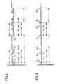
- Fig. is a graph illustrating predetermined complementary patterns P and P' which are written many times around a track of a disk. It will be noted that the complementary patterns P and P' differ in that corresponding transitions of P and P' are in opposite directions in Fig. 1. As shown, each pattern (P or P') comprises a first transition (TR1 or TR1') followed by a relatively widely spaced second transition (TR2 or TR2') which in turn is followed by a relatively closely spaced transistion (TR3 or TR3').
- relatively closely spaced transitions TR2, TR3 and TR2', TR3' in patterns P and P' are chosen to have respective spacings TP4 and TP4' corresponding.to the closest transition spacing to be detected by the head being tested, while the relatively widely spaced transitions TR1, TR2 and TR1', TR2' in patterns P and P' are chosen to have respective spacings TP1 and TP1' such that the detected location obtained for transitions TR1 and TR1' on readback will not be affected by adjacent transitions.
- the respective spacings TP3 and TP3' between patterns P and P' are likewise chosen so that the transitions in adjacent patterns P and P' do not affect the detected locations of transitions TR1 and TR1'.
- Fig. 2 illustrates typical detected pulses R1, R2, R3 and R1', R2', R3' derived from readback of the respective corresponding transitions TR1, TR2, TR3 and TR1', TR2', TR3' in the patterns P and P' in Fig. 1.
- the most significant time interval measurements are the time intervals T1, T2 and T3 for pattern P and the time intervals T1', T2' and T3' for pattern P', which correspond to transition spacings TP1, TP2, TP3, TP1', TP2' and TP3', respectively, in Fig. 1.
- Fig. 1 As shown in Fig.
- T1 is the time interval between the detection of pulses R2 and R1
- T2 is the time interval between the detection of pulses R3 and R1
- T3 is the time interval between the detection of pulses R1' and R1.
- T1' is the time interval between the detection of pulses R2' and R1'
- T2' is the time interval between the detection of pulses R3' and R1'
- T3' is the time interval between the detection of pulses R1 and R1'.
- FIG. 3 illustrates a particular example of preferred apparatus in accordance with the invention.
- a rotatable magnetic disk 10 is provided of the type which is to be used with the magnetic heads to be tested.
- the disk 10 can be prewritten with the patterns P and P' (Fig. 1) in pattern track 10a, or else, these patterns could be written in pattern track 10a by the head 12 under test in order to test the head's write performance.
- Writing of the patterns P and P' in track 10a is accomplished using a timing track 10b which is read by a magnetic head 11 (or some other suitable tranducer) to provide disk timing signals to timing circuitry 13 for providing appropriate timing signals (synchronized with disk rotation) to a conventional form of signal data generator 15.
- the signal data generator 15 operates in response to input control signals from a conventional programmable signal source 16 for applying predetermined pattern signals (corresponding to P and P' in Fig. 1) to conventional write circuitry 17 which, in response to timing signals from timing circuitry 13, provides appropriate write signals 17a to a magnetic head 19 for writing the patterns P and P' (Fig. 1) in the pattern track 10a.
- the head 19 when read performance is to be tested, the head 19 is caused to read the patterns P and P' (Fig. 1) in the pattern track 10a and the resultant head output is applied to conventional read circuitry 22 which produces detected output pulses R1, R2, R3, R1', R2', R3', such as illustrated in Fig. 2.
- the read circuitry 22 may also receive disk timing signals from timing circuitry 13. The speed of rotation of the disk 10 should preferably be the same as that which will be used when the system is operated.
- time interval detector 25 which serves as a pattern recognizer and is capable of distinguishing the applied pulses R1, R2, R3, R1', R2', R3'.
- time interval detector 25 produces start and stop output signals corresponding to the beginning and end, respectively, of particular selected timing intervals occuring between the applied pulses R1, R2, R3, R1', R2', R3'.
- the start and stop output signals produced by the time interval selector 25 are in turn applied to timer instrumentation circuitry 30 which may also be of conventional form.
- the timer instrumentation circuitry 30 operates in a conventional manner to accurately measure the time between each corresponding pair of start and stop pulses received from the time interval detector 25 and to apply signals, representative of the resulting time interval measurements to analyzing circuitry 40.
- the analyzing circuitry 40 also receives signals from source 16 related to the time intervals between particular ones of the transistions TR1, TR2, TR3, TR1', TR2', TR3' of the patterns P and P' shown in Fig. 1.
- the important timing intervals to be analyzed are the recorded transition intervals TP1, TP2, TP3, TP1', TP2', TP3' of patterns P and P' (Fig. 1) and the corresponding playback time intervals T1, T2, T3, T1', T2', T3' derived from pulses R1, R2, R3, R1', R2', R3' (Fig. 2).
- a measurement of timing asymmetry can also be derived.
- the time interval detector 25 is adapted to provide start and stop output signals to the timer instrumentation circuitry 30 corresponding to the playback timing intervals T1, T2, T3, T1', T2', T3' intervals in Fig. 2, and the signal source 16 is caused to provide signals to the analyzing circuitry 40 representative of the corresponding recorded transition intervals TP1, TP2, TP3, TP1', TP2', TP3'.
- the analyzer 40 may be implemented by hardware, by an appropriately programmed computer, or by a combination of both.
- the various analyzer functions will be illustrated as being implemented by readily providable components, such as illustrated in Figs. 4-7. From the description provided, one skilled in the art will readily be able to provide an appropriately programmed computer to perform all or any desired portion of these analyzer functions.
- the pattern induced left and right bit shifts are advantageously derived by averaging the differences measured between the respective intervals TP1 and T1 and TP1' and T1' (for left pattern induced bit shift) and between TP2 and T2 and TP2' and T2' (for right pattern induced bit shift) of the many patterns P and P' recorded around the pattern track 10a (Fig. 3), thereby substantially removing bit shift effects caused by media irregularities and noise.
- Fig. 4 An exemplary implementation which may be provided in the analyzer 40 for obtaining pattern induced bit shift in accordance with the foregoing is illustrated in Fig. 4. It will be seen in Fig. 4 that for this purpose the analyzer 40 includes difference circuits 41 and 42 feeding averaging circuits 44 and 45, respectively.
- the difference circuit 41 receives signals S1 from the timer instrumentation circuitry 30 which are representative of the time intervals T1 and T1' and also receives signals SP1 from the signal source 16 which are respresentative of the time intervals TP1 and TP1'.
- the difference circuit 42 receives signals S2 which are representative of the time intervals T2 and T2' from the timer instrumentation circuitry 30 and also receives signals SP2 from the signal source 16 which are representative of the time intervals TP2 and TP2'.
- These difference circuits 41 and 42 operate to successively produce output signals 41a and 42a, respectively, which are representative of the measured differences obtained between corresponding ones of the applied time intervals as the disk 10 is rotated.
- These output signals 41 a and 42a produced by the difference circuits 41 and 42, respectively, are applied to respective averaging circuits 44 and 45 to produce output signals 44a and 45a representative of the average of the measured differences applied thereto. From the previous discussion, it will be understood that the output signals 44a and 45a thus respectively represent the pattern induced left and right bit shifts.
- Fig. 5 is an exemplary implementation which may be provided in the analyzer 40 in Fig. 3 for measuring noise induced bit shift.
- the jitter of the pulse can be determined. Noise detection apparatus for obtaining jitter in this manner are well known in the art.
- the jitter on the readback pulses is advantageously employed as an indication of noise induced bit shift. Accordingly, while the disk is rotating, time instrumentation circuitry 30 in Fig.
- the noise detection apparatus 52 for determining the jitter on the individual readback pulses as the disk is rotated.
- the jitter output signal 52a produced by the noise detection apparatus is applied to conventional statistical calcuation apparatus 54 to obtain an indication of the standard deviation of the jitter. In the preferred embodiment of the invention being considered, this standard deviation is used as a measure of noise induced bit shift.
- timing asymmetry is present when the measured interval between the readback of a first occurring positive-going transition of a recorded pattern and the readback of a later occurring negative-going transition is different from the time interval between the readback of a first occuring negative-going transition and the readback of a later occurring positive-going transition.
- each time interval T1 in Fig. 2 is an example of a readback time interval corresponding to a recorded time interval (TP1 in Fig. 1) which begins with a positive-going transition (TR1) and ends with a negative-going transition (TR2)
- each time interval T1' in Fig. 2 is an example of a readback time interval corresponding to a recorded time interval (TP1') which begins with a negative-going transition (TR1') and ends with a positive-going transistion (TR2').
- readback intervals T3 and T3' have the same relationship as intervals T1 and T1' in this regard.
- the jitter detected between T1 and T1' or between T3 and T3' will be dependent upon head timing asymmetry. However, this jitter will also be affected by noise.
- the jitter detected between T1 and T1' or between T3 and T3' is compared with the jitter detected for the time interval T2 or T2', which is essentially unaffected by timing asymmetry (since both T2 and T2') correspond to beginning and ending transitions which change in the same direction).
- the timing instrumentation circuitry 30 applies signals Y representative of at least one pair of the intervals T1 and T1' orT3 and T3' and at least one of the intervals T2 or T2' to noise detection apparatus 52 which may be the same as illustrated in Fig. 5.
- the noise detection apparatus 52 determines the comparative jitter between T2 orT2' and the applied pair T1 and T1' or T3 and T3' and applies a resultant jitter signal 52b corresponding thereto to statistical calculation apparatus 54 which may also be the same as illustrated in Fig. 5.
- the standard deviation of this jitter signal 52b is used as an indication of timing asymmetry.
- the time intervals T2 and T2' in Fig. 2 are essentially unaffected by any timing asymmetry. However, these intervals are affected by noise, thereby providing a convenient way of also determining noise.
- the timer instrumentation circuiry 30 applies signals H representative of at least one of the intervals T2 or T2' to noise detection apparatus 52 which in turn provides a jitter signal 52c to statistical calculation apparatus 54.
- the standard deviation of this jitter signal is used as an indication of bit shift caused by noise.
- the noise cancellation apparatus 52 and the statistical calculation apparatus 54 may be the same as in Figs. 5 and 6.
- Fig. 8 illustrating an improvement over the embodiment of Fig. 3 which provides for calibrating the system using the same write signals as used for writing the patterns P and P' in Fig. 1.
- the difference between the embodiments of Figs. 3 and 8 resides in the provision of a switch 110 at the input to the read circuitry 22 which permits selecting either read signals from the head 19 or write signals from the write circuitry 17 applied via an attenuator 112 and a differentiator 114.
- the purpose of the attenuator 112 and differentiator 114 isto convert the write signals into "idealized" read signals for calibrating the system.
- the switch 110 is placed in its calibrate position to receive the "idealized" read signals provided at the output of the differentiator 114, and the various measurements previously described are then obtained. The differences between these measurements and those obtained for actual read signals will then provide more accurate resultant values.
Landscapes
- Engineering & Computer Science (AREA)
- Signal Processing (AREA)
- Multimedia (AREA)
- Digital Magnetic Recording (AREA)
- Investigating Or Analyzing Materials By The Use Of Magnetic Means (AREA)
- Measuring Magnetic Variables (AREA)
Claims (3)
Applications Claiming Priority (2)
| Application Number | Priority Date | Filing Date | Title |
|---|---|---|---|
| US61743784A | 1984-06-05 | 1984-06-05 | |
| US617437 | 1984-06-05 |
Publications (2)
| Publication Number | Publication Date |
|---|---|
| EP0167284A1 EP0167284A1 (de) | 1986-01-08 |
| EP0167284B1 true EP0167284B1 (de) | 1989-10-18 |
Family
ID=24473643
Family Applications (1)
| Application Number | Title | Priority Date | Filing Date |
|---|---|---|---|
| EP19850303887 Expired EP0167284B1 (de) | 1984-06-05 | 1985-06-03 | Prüfverfahren für Bestandteile eines magnetischen Speichersystems |
Country Status (3)
| Country | Link |
|---|---|
| EP (1) | EP0167284B1 (de) |
| JP (1) | JPS61105778A (de) |
| DE (1) | DE3573855D1 (de) |
Families Citing this family (1)
| Publication number | Priority date | Publication date | Assignee | Title |
|---|---|---|---|---|
| EP2541250A1 (de) * | 2011-06-30 | 2013-01-02 | Koninklijke Philips Electronics N.V. | Molekulare Architektur von magnetischen Partikeln für Affinitätsprüfungen mit geringer nicht spezifischer Bindung |
Family Cites Families (5)
| Publication number | Priority date | Publication date | Assignee | Title |
|---|---|---|---|---|
| US3686682A (en) * | 1970-08-17 | 1972-08-22 | Burroughs Corp | Method and apparatus for testing magnetic disc files |
| US3996612A (en) * | 1975-07-07 | 1976-12-07 | Ncr Corporation | Test code generator |
| US4009490A (en) * | 1975-07-07 | 1977-02-22 | Ncr Corporation | PLO phase detector and corrector |
| US4142215A (en) * | 1977-12-02 | 1979-02-27 | The Telex Corporation | Tape drive tester |
| JPS60117631A (ja) * | 1983-11-30 | 1985-06-25 | Toshiba Corp | 化合物半導体のドライエッチング方法 |
-
1985
- 1985-05-30 JP JP11763285A patent/JPS61105778A/ja active Pending
- 1985-06-03 EP EP19850303887 patent/EP0167284B1/de not_active Expired
- 1985-06-03 DE DE8585303887T patent/DE3573855D1/de not_active Expired
Also Published As
| Publication number | Publication date |
|---|---|
| EP0167284A1 (de) | 1986-01-08 |
| DE3573855D1 (en) | 1989-11-23 |
| JPS61105778A (ja) | 1986-05-23 |
Similar Documents
| Publication | Publication Date | Title |
|---|---|---|
| EP0168155B1 (de) | Prüfverfahren für Bestandteile eines magnetischen Speichersystems | |
| US3686682A (en) | Method and apparatus for testing magnetic disc files | |
| US5357520A (en) | Method and apparatus for precompensation value determination in a PRML data channel | |
| US4454549A (en) | Slant track sector servo | |
| US5068754A (en) | Method and apparatus for measuring bit shift | |
| US4796109A (en) | Method for testing components of a magnetic storage system | |
| US5109304A (en) | Method of apparatus for detecting defects in data apparatus such as magnetic storage apparatus | |
| EP0950245B1 (de) | Verfahren und gerät zur aufzeichnung einer taktspur auf einem aufzeichnungsmedium | |
| US3755731A (en) | System for detecting dropout and noise characteristics of magnetic tape with switch means to select which characteristics to be detected | |
| US4672483A (en) | Information recording and reading apparatus having recording error checking circuit | |
| US4574234A (en) | System for measuring selected parameters of electrical signals and method | |
| US4651105A (en) | Digital peak detecting means for a pulse train of electrical signals having a frequency within a known frequency bandwidth | |
| EP0167284B1 (de) | Prüfverfahren für Bestandteile eines magnetischen Speichersystems | |
| US5872664A (en) | Distortion of an isolated pulse | |
| US20030142435A1 (en) | Magnetic disk apparatus, magnetic recording medium and method of servo waiting | |
| JP3924405B2 (ja) | データ・ブロックの書き込み方法、装置、及び記憶媒体 | |
| US4651102A (en) | Method of converting a pulse train of electrical signals into digital signals | |
| US4686470A (en) | Magnetic disk for measuring the azimuth of a transducer head | |
| JP2954104B2 (ja) | バルクハウゼンノイズ検出方法 | |
| JP3057282B2 (ja) | デジタル記録再生特性評価方法 | |
| KR930004218B1 (ko) | 자기 기록장치의 타임마진 측정방법 | |
| US3668665A (en) | Apparatus for ensuring timing track accuracy | |
| JP2547608B2 (ja) | ヘッド位置制御方法 | |
| JP2802816B2 (ja) | サーボディスクの媒体検査方式 | |
| JPS59191117A (ja) | 磁気記憶装置 |
Legal Events
| Date | Code | Title | Description |
|---|---|---|---|
| PUAI | Public reference made under article 153(3) epc to a published international application that has entered the european phase |
Free format text: ORIGINAL CODE: 0009012 |
|
| 17P | Request for examination filed |
Effective date: 19850614 |
|
| AK | Designated contracting states |
Designated state(s): DE FR GB |
|
| 17Q | First examination report despatched |
Effective date: 19870625 |
|
| RAP1 | Party data changed (applicant data changed or rights of an application transferred) |
Owner name: UNISYS CORPORATION |
|
| GRAA | (expected) grant |
Free format text: ORIGINAL CODE: 0009210 |
|
| AK | Designated contracting states |
Kind code of ref document: B1 Designated state(s): DE FR GB |
|
| ET | Fr: translation filed | ||
| REF | Corresponds to: |
Ref document number: 3573855 Country of ref document: DE Date of ref document: 19891123 |
|
| PLBE | No opposition filed within time limit |
Free format text: ORIGINAL CODE: 0009261 |
|
| STAA | Information on the status of an ep patent application or granted ep patent |
Free format text: STATUS: NO OPPOSITION FILED WITHIN TIME LIMIT |
|
| 26N | No opposition filed | ||
| PGFP | Annual fee paid to national office [announced via postgrant information from national office to epo] |
Ref country code: FR Payment date: 19940613 Year of fee payment: 10 |
|
| PG25 | Lapsed in a contracting state [announced via postgrant information from national office to epo] |
Ref country code: FR Effective date: 19960229 |
|
| REG | Reference to a national code |
Ref country code: FR Ref legal event code: ST |
|
| PGFP | Annual fee paid to national office [announced via postgrant information from national office to epo] |
Ref country code: GB Payment date: 19970506 Year of fee payment: 13 |
|
| PG25 | Lapsed in a contracting state [announced via postgrant information from national office to epo] |
Ref country code: GB Free format text: LAPSE BECAUSE OF NON-PAYMENT OF DUE FEES Effective date: 19980603 |
|
| PGFP | Annual fee paid to national office [announced via postgrant information from national office to epo] |
Ref country code: DE Payment date: 19980625 Year of fee payment: 14 |
|
| GBPC | Gb: european patent ceased through non-payment of renewal fee |
Effective date: 19980603 |
|
| PG25 | Lapsed in a contracting state [announced via postgrant information from national office to epo] |
Ref country code: DE Free format text: LAPSE BECAUSE OF NON-PAYMENT OF DUE FEES Effective date: 20000503 |