EP0167302B1 - Antennenspeiseschaltungen - Google Patents
Antennenspeiseschaltungen Download PDFInfo
- Publication number
- EP0167302B1 EP0167302B1 EP85304020A EP85304020A EP0167302B1 EP 0167302 B1 EP0167302 B1 EP 0167302B1 EP 85304020 A EP85304020 A EP 85304020A EP 85304020 A EP85304020 A EP 85304020A EP 0167302 B1 EP0167302 B1 EP 0167302B1
- Authority
- EP
- European Patent Office
- Prior art keywords
- phase
- network according
- feed network
- slope
- waveguide section
- Prior art date
- Legal status (The legal status is an assumption and is not a legal conclusion. Google has not performed a legal analysis and makes no representation as to the accuracy of the status listed.)
- Expired - Lifetime
Links
- 230000010363 phase shift Effects 0.000 claims description 26
- 230000001939 inductive effect Effects 0.000 claims description 23
- 238000013461 design Methods 0.000 description 6
- 238000010586 diagram Methods 0.000 description 5
- 229910052751 metal Inorganic materials 0.000 description 3
- 239000002184 metal Substances 0.000 description 3
- 238000013459 approach Methods 0.000 description 2
- 238000000926 separation method Methods 0.000 description 2
- 229910052782 aluminium Inorganic materials 0.000 description 1
- XAGFODPZIPBFFR-UHFFFAOYSA-N aluminium Chemical compound [Al] XAGFODPZIPBFFR-UHFFFAOYSA-N 0.000 description 1
- 239000003990 capacitor Substances 0.000 description 1
- 238000004891 communication Methods 0.000 description 1
- 238000010276 construction Methods 0.000 description 1
- 238000012937 correction Methods 0.000 description 1
- 238000009826 distribution Methods 0.000 description 1
- 238000004519 manufacturing process Methods 0.000 description 1
- 229940050561 matrix product Drugs 0.000 description 1
- 238000000034 method Methods 0.000 description 1
- 238000012552 review Methods 0.000 description 1
Images


Classifications
-
- H—ELECTRICITY
- H01—ELECTRIC ELEMENTS
- H01P—WAVEGUIDES; RESONATORS, LINES, OR OTHER DEVICES OF THE WAVEGUIDE TYPE
- H01P1/00—Auxiliary devices
- H01P1/18—Phase-shifters
- H01P1/182—Waveguide phase-shifters
-
- H—ELECTRICITY
- H01—ELECTRIC ELEMENTS
- H01P—WAVEGUIDES; RESONATORS, LINES, OR OTHER DEVICES OF THE WAVEGUIDE TYPE
- H01P1/00—Auxiliary devices
- H01P1/20—Frequency-selective devices, e.g. filters
- H01P1/207—Hollow waveguide filters
Definitions
- This invention relates to a feed network for a microwave antenna of the type having a plurality of individual antenna components for sending or receiving signals in predetermined phase offsets relative to one another, the feed network comprising individual feed lines connected respectively to the individual antenna components and devices connected in the feed lines such that the predetermined phase offsets are achieved across the bandwidth.
- phase shifters are of two types, namely inductive and capacitive, to ensure not only correct phase at midband but also to achieve equal phase slope among the many runs leading to the antenna horns.
- phase shifters are used in a typical communication satellite; for example the G-STAR antenna has over a hundred phase shifters.
- phase shifter represents a major component in the overall cost of the feed network and the space occupied by the phase shifters significantly increases the size of the feed network.
- the present invention seeks to replace the phase shifter in the antenna feed network with a device which is smaller and simpler than the phase shifter and which is required in fewer numbers than the phase shifter in any one feed network, thereby reducing the cost and size of the feed network.
- the present invention is characterized in that the predetermined phase offsets in the region of the midband frequency are defined by the relative lengths of the feed lines, each feed line having a phase shift/frequency response characteristic, the slope of which is determined by the length of the feed line and the network includes, in at least each feed line which has a lesser said slope than the feed line having the greatest said slope, a phase slope equalizer having a substantially constant slope phase shift/frequency response characteristic extending from a positive phase shift through zero phase shift in the region of the midband frequency to a negative phase shift, the slope of the phase shift/frequency frequency response characteristic of each said phase slope equalizer being equal to the difference in slope between the phase shift/frequency response characteristic of the feed line containing said phase slope equalizer and the phase shift/frequency response characteristic of the line with the greatest said slope.
- phase slope equalizer The novel device, known hereinafter as a phase slope equalizer, is placed in each run of the antenna.
- the phase slope equalizer comprises, in essence, a resonant circuit placed in a waveguide.
- the resonant circuit is a parallel resonant circuit comprising a pair of inductive posts with a capacitive tuning screw located between the posts.
- an inductive iris is used.
- the capacitive element is a tuning screw.
- a third embodiment is in the form of a resonant slot which replaces both the inductive posts and the capacitive tuning screw.
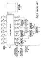
- FIGURE 1 The significance of the invention will be better understood after a brief review of a conventional prior art antenna feed network as shown in FIGURE 1.
- the antenna feed network comprises a horn array 2, a duplexer (also known as diplexer) array 4, a transmit network 6 and a receive network 8.
- the horn array 2 comprises a plurality (eight illustrated in this example) of individual horns 2a-2h all of which are positioned to direct individual radio frequency beams onto a reflector (not shown) which redirects a combined beam to the desired coverage area on earth.
- the duplexer array 4 simply provides a means for allowing the transmit 6 and receive 8 networks to share the same array of horns, and for the purposes of understanding the present invention, need not be described further herein.
- the transmit network 6 is similar in detailed construction and operation to the receive network 8 and, accordingly, only the transmit network will be described in greater detail.
- the transmit network 6 are a plurality of couplers 12 and phase shifters 14.
- the couplers 12 distribute power among the horns 2a-2h in a prescribed manner. By varying the line lengths appropriately and by selecting appropriate phase shifters 14, the desired phase relationship among the horns may be achieved. Although two phase shifters 14 are shown in each feed line 16, the lines may have more than two phase shifters.
- the phase shifters 14 used are of two types, capacitive and inductive. These give respectively negative and positive phase offsets. The phase offset however varies with frequency. Thus, if a 90 ° phase difference is required between two lines, a single 90 ° phase shifter placed in one of the lines will give the correct phase relationship at one frequency only, say at midband; there will be an error at the bandedges. To avoid this error, it is necessary to use a +45° phase shifter in one line and a -45° phase shifter in the other.
- the two phase shifters although having differing signs, both have the same phase slope. That is, a capacitive phase shifter having numerically the same phase offset at midband as that of an inductive phase shifter, will also have the same algebraic slope. In a typical feed therefore, combinations of different capacitive and inductive phase shifters are used throughout.
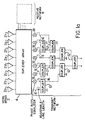
- phase slope equalizer a new component that has zero phase offset at midband but has a substantially constant phase slope across the bandwidth.
- Phase correction therefore becomes relatively simple.
- the path lengths of the various feed lines are arranged to give the required phase offsets at midband only and then phase slope equalizers (one per line) are introduced to equalize the slopes among the lines 16.
- the slopes of all these equalizers have the same sign. This new approach dispenses with the inductive and capacitive phase shifters 14.
- each feed line 16 has a sloping phase shift/frequency response characteristic the slope of which is determined by the length of the feed line.
- a phase slope equalizer 18 is inserted into each feed line 16 except for that feed line the phase shift/frequency response characteristic of which has the greatest slope.
- the leftmost feed line 16' is assumed to have the greatest length and hence the greatest offset and slope. Accordingly, it obviously does not need and therefore does not include a phase slope equalizer.
- FIGURES 2(a) and 2(b) illustrate an example of the new phase slope equalizer 18. It comprises a rectangular section waveguide 20 across the smaller dimension of which extend two metal posts 22 which are both soldered to opposite faces 24 and 26 of the waveguide 20.
- a metal tuning screw 28 is received in a threaded hole (not shown) in face 26 of waveguide 20 and extends inwardly of the waveguide at a location intermediate the posts 22 and parallel thereto.
- a portion of screw 28 extends outwardly of the wave guide and is provided with a slot 30 which may be engaged by a screwdriver for moving the screw further inwardly or outwardly to increase or decrease the capacitance as necessary to tune the device to the midband frequency.
- FIGURE 3 is the equivalent diagram of the phase slope equalizer 18 of FIGURES 2(a) and 2(b). Essentially the device operates as a shunt resonator comprising an inductance L representing the inductance of the posts 22 and a variable capacitor C representing the variable capacitance of the tuning screw 28.
- phase shift/frequency response curve 32 is essentially a straight line passing through the midband frequency f0 at zero phase offset, the slope of the line being negative, substantially constant and a function of L and C.
- the more the midband frequency f0 exceeds a given frequency the more positive is the phase shift ⁇ and the more a given frequency exceeds f0 the more negative is the phase shift ⁇ .
- FIGURE 5 When the circuit of FIGURE 3 is connected in a line it may be represented by FIGURE 5 in which jB represents the impedance of the shunt resonator, E1 is the input voltage and E2 is the output voltage.
- the return loss can be improved by using two smaller elements, each giving half the slope, separated by quarter wave-length as shown in FIGURE 6.
- the waveguide, posts and screws are made of aluminum, the waveguide is 0.75" (19.05mm) wide, the posts 0.062" (1.58mm) in diameter and the screws 0.20" (5.8mm) in diameter.
- the quarter wavelength distance between the elements corresponds to 0.328" (8.33mm).
- Small phase slope can of course be compensated by a single element. Conversely in situations where larger than ⁇ 5°/500 MHz slope is required, then 3- or 4- element designs could be used.
- each having twice the susceptance of that of the first (or last) element For designs with more than two elements it is preferred, for performance reasons, to have all the inner elements, each having twice the susceptance of that of the first (or last) element. For example, if the susceptance B0 of the first (or last) element is equal to 5, then all of the other elements should each have a susceptance of 10. The spacing between consecutive elements is quarter-wave at the midband.
- the first element and the last element each comprises a pair of spaced posts 22 and a tuning screw 28 of the type shown schematically in FIGURES 2(a) and 2(b).
- the second and third elements spaced from each other and from the first and last elements by a quarter wavelength, each comprises a pair of spaced posts 42 of greater diameter than posts 22 to provide an inductance twice that of posts 22 and a tuning screw 44 of greater length than screws 28 to provide a capacitance twice that of screws 28.
- FIGURE 10 showing a 4-element design can be used. This has the two inner elements spaced half-wave apart. In essence, the first two elements form a pair, whose centre is spaced three quarter-wave from the centre of the pair formed by the third and last elements. It is recommended, for designs with even more than 4 elements, that the former (i.e. every spacing is quarter-wave) be used.
- phase slope equalizer is shown in FIGURES 7(a) and 7(b).
- an inductive iris 36 is used instead of inductive posts.
- the iris is formed as a thin metal plate defining an aperture 37 into which extends the tuning screw 28.
- FIGURES 8(a) and 8(b) A further alternative is shown in FIGURES 8(a) and 8(b).
- the posts and tuning screw are replaced with a resonant slot 38 which resonates at the midband frequency.
- the embodiments using an inductive iris or resonant slot may be provided with two or more elemental resonant circuits.
- the same considerations regarding spacing and susceptance as discussed in relation to FIGURES 9 and 10 apply to the multi-element iris or resonant slot type.
- phase slope equalizer two basic embodiments have been described.
- the first is where the inner elements are identical but of double the susceptance of the first (and last) element.
- the second is where all the elements are identical but their separations are unequal.
- other distributions of element values i.e. unequal elements
- the separation between elements is essentially quarter-wave or multiples of quarter-wave.
Landscapes
- Variable-Direction Aerials And Aerial Arrays (AREA)
- Control Of Motors That Do Not Use Commutators (AREA)
Claims (16)
- Speisenetzwerk für eine Mikrowellenantenne des Typs mit einer Vielzahl von individuellen Antennenkomponenten zum Senden oder Empfangen von Signalen in vorbestimmten, zueinander gegenseitigen Phasenverschiebungen, wobei das Speisenetzwerk aufweist:
individuelle Zuführleitungen (16), welche jeweils an die individuellen Antennenkomponenten (2a bis 2n) angeschlossen sind, und Vorrichtungen (14), welche in den Zuführleitungen so angeschlossen sind, daß die vorbestimmten Phasenverschiebungen durch die Bandweite erreicht werden,
dadurch gekennzeichnet, daß
die vorbestimmten Phasenverschiebungen in dem Gebiet des mittleren Frequenzbandes durch die relativen Längen der Zuführleitungen (16, 16') definiert sind, wobei jede Zuführleitung eine Phasenverschiebung/Frequenz-Antwort-Kennlinie hat, deren Steigung durch die Länge der Zuführleitung (16, 16') bestimmt ist, und das Netzwerk beinhaltet in zumindest jeder Zuführleitung (16), welche eine geringere Steigung als die Zuführleitung (16') mit der größten Steigung hat,
eine Phasensteigungs-Entzerrvorrichtung (18) mit einer im wesentlichen konstanten Steigungs-Phasenverschiebungs-/Frequenz-Antwort-Kennlinie, welche sich von einer positiven Phasenverschiebung über eine Null-Phasenverschiebung in das Gebiet des mittleren Frequenzbandes zu einer negativen Phasenverschiebung erstreckt, wobei die Steigung der Phasenverschiebung/Frequenz-Antwort-Kennlinie von jeder Phasensteigungs-Entzerrvorrichtung (18) gleich ist der Differenz der Steigung zwischen der Phasenverschiebungs/Frequenz-Antwort-Kennlinie der Zuführleitung (16), welche die Phasensteigungs-Entzerrvorrichtung enthält, und der Phasenverschiebung/Frequenz-Antwort-Kennlinie der Leitung (16') mit der größten Steigung. - Speisenetzwerk nach Anspruch 1, dadurch gekennzeichnet, daß jede der Phasensteigungs-Entzerrvorrichtung (18) einen Wellenleiterabschnitt (20) aufweist, der einen Schwingkreis (C, L) enthält.
- Speisenetzwerk nach Anspruch 2, dadurch gekennzeichnet, daß der Schwingkreis ein Parallelstromkreis (C, L) ist.
- Speisenetzwerk nach Anspruch 3, dadurch gekennzeichnet, daß der Schwingkreis zwei mit Zwischenraum angeordnete induktive Stäbe (22) aufweist, welche sich über den Wellenleiterabschnitt (20) erstrecken, und eine kapazitive Abstimmschraube (28), welche in einem Gewindeloch in dem Wellenleiterabschnitt (20) enthalten ist, und sich in das Innere des Wellenleiterabschnitts erstreckt, und zwar an einem Ort zwischen den Stäben und parallel zu ihnen.
- Speisenetzwerk nach Anspruch 3, dadurch gekennzeichnet, daß der Schwingkreis eine induktive Blende (36) aufweist, welche sich in dem Wellenleiterabschnitt befindet und eine Öffnung (37) definiert, und eine kapazitive Abstimmschraube (28), welche in einem Gewindeloch in dem Wellenleiterabschnitt (20) enthalten ist und sich in das Innere des Wellenleiterabschnitts (20) erstreckt, und zwar an dem Ort der Öffnung (37).
- Speisenetzwerk nach Anspruch 3, dadurch gekennzeichnet, daß der Schwingkreis einen Resonanzschlitz (38) aufweist, der sich in dem Wellenleiterabschnitt (20) befindet.
- Speisenetzwerk nach Anspruch 3, dadurch gekennzeichnet, daß der Schwingkreis aus einer Vielzahl von identischen Elementschwingkreisen gebildet ist.
- Speisenetzwerk nach Anspruch 4, dadurch gekennzeichnet, daß zusätzlich zu dem Satz zweier induktiver Stäbe (22) und einer kapazitiven Abstimmschraube (28), der Wellenleiterabschnitt (20) auch einen weiteren oder mehrere Sätze zweier induktiver Stäbe (42) und eine kapazitive Abstellschraube (44) beherbergt, wobei die verschiedenen Sätze voneinander durch vorbestimmte Intervalle entlang des Wellenleiterabschnitts (20) getrennt sind.
- Speisenetzwerk nach Anspruch 8, dadurch gekennzeichnet, daß sämtliche Sätze (22, 28) den gleichen Blindleitwert haben, daß der Abstand zwischen jedem äußeren Satz und seinem nächsten Satz eine Viertel-Wellenlänge ist und daß der Abstand zwischen zwei beliebigen aufeinanderfolgenden inneren Sätzen eine Viertel-Wellenlänge oder ein Vielfaches einer Viertel-Wellenlänge ist.
- Speisenetzwerk nach Anspruch 8, dadurch gekennzeichnet, daß der Blindleitwert jedes äußeren Satzes die Hälfte ist von dem jedes inneren Satzes und daß der Abstand zwischen aufeinanderfolgenden Sätzen eine Viertel-Wellenlänge ist.
- Speisenetzwerk nach Anspruch 5, dadurch gekennzeichnet, daß zusätzlich zu dem Satz der induktiven Blende (36) und kapazitiven Abstimmschraube (28), der Wellenleiterabschnitt (20) auch eine weitere oder mehrere Sätze einer induktiven Blende (36) und einer kapazitiven Abstimmschraube (28) beherbergt, wobei die verschiedenen Sätze durch vorbestimmte Intervalle entlang des Wellenleiterabschnitts (20) getrennt sind.
- Speisenetzwerk nach Anspruch 11, dadurch gekennzeichnet, daß alle Sätze (36, 38) den gleichen Blindleitwert haben, der Abstand zwischen jedem äußeren Satz und seinem nächsten inneren Satz eine Viertel-Wellenlänge ist und der Abstand zwischen zwei beliebigen aufeinanderfolgenden inneren Sätzen eine Viertel-Wellenlänge oder ein Vielfaches einer Viertel-Wellenlänge ist.
- Speisenetzwerk nach Anspruch 11, dadurch gekennzeichnet, daß der Blindleitwert jedes äußeren Satzes die Hälfte ist von dem eines inneren Satzes und der Abstand zwischen aufeinanderfolgenden Sätzen eine Viertel-Wellenlänge ist.
- Speisenetzwerk nach Anspruch 6, dadurch gekennzeichnet, daß zusätzlich zu dem Resonanzschlitz (38), der Wellenleiterabschnitt (20) auch einen weiteren oder weitere Resonanzschlitze (38) beherbergt, wobei die Resonanzschlitze (38) durch vorbestimmte Intervalle entlang des Wellenleiterabschnitts (20) getrennt sind.
- Speisenetzwerk nach Anspruch 14, dadurch gekennzeichnet, daß samtliche Schlitze (38) denselben Blindleitwert haben, der Abstand zwischen jedem äußeren Schlitz und seinem nächsten Schlitz eine Viertel-Wellenlänge ist und der Abstand zwischen zwei beliebigen aufeinanderfolgenden inneren Schlitzen eine Viertel-Wellenlänge oder ein Vielfaches einer Viertel-Wellenlänge ist.
- Speisenetzwerk nach Anspruch 14, dadurch gekennzeichnet daß der Blindleitwert jedes äußeren Schlitzes die Hälfte ist von dem jedes inneren Schlitzes und der Abstand zwischen aufeinanderfolgenden Schlitzen eine Viertel-Wellenlänge ist.
Applications Claiming Priority (2)
| Application Number | Priority Date | Filing Date | Title |
|---|---|---|---|
| US618446 | 1984-06-07 | ||
| US06/618,446 US4633258A (en) | 1984-06-07 | 1984-06-07 | Phase slope equalizer |
Publications (3)
| Publication Number | Publication Date |
|---|---|
| EP0167302A2 EP0167302A2 (de) | 1986-01-08 |
| EP0167302A3 EP0167302A3 (en) | 1987-09-09 |
| EP0167302B1 true EP0167302B1 (de) | 1992-01-15 |
Family
ID=24477722
Family Applications (1)
| Application Number | Title | Priority Date | Filing Date |
|---|---|---|---|
| EP85304020A Expired - Lifetime EP0167302B1 (de) | 1984-06-07 | 1985-06-06 | Antennenspeiseschaltungen |
Country Status (4)
| Country | Link |
|---|---|
| US (1) | US4633258A (de) |
| EP (1) | EP0167302B1 (de) |
| CA (1) | CA1234912A (de) |
| DE (2) | DE167302T1 (de) |
Families Citing this family (6)
| Publication number | Priority date | Publication date | Assignee | Title |
|---|---|---|---|---|
| CA1260083A (en) * | 1986-12-04 | 1989-09-26 | Chuck K. Mok | Phase slope equalizer for satellite attennas |
| FR2634949B1 (fr) * | 1988-07-28 | 1991-01-04 | Alcatel Thomson Faisceaux | Filtre large bande en guide d'onde |
| JP2607780B2 (ja) * | 1991-09-18 | 1997-05-07 | 富士通株式会社 | 導波管形フィルタ装置 |
| US9007275B2 (en) * | 2006-06-08 | 2015-04-14 | Fractus, S.A. | Distributed antenna system robust to human body loading effects |
| US10170831B2 (en) * | 2015-08-25 | 2019-01-01 | Elwha Llc | Systems, methods and devices for mechanically producing patterns of electromagnetic energy |
| EP4250485A4 (de) * | 2020-12-28 | 2024-01-17 | Huawei Technologies Co., Ltd. | Basisstationsantenne |
Family Cites Families (17)
| Publication number | Priority date | Publication date | Assignee | Title |
|---|---|---|---|---|
| US102002A (en) * | 1870-04-19 | Gheister l | ||
| US2461005A (en) * | 1940-04-05 | 1949-02-08 | Bell Telephone Labor Inc | Ultra high frequency transmission |
| US2642529A (en) * | 1949-07-29 | 1953-06-16 | Int Standard Electric Corp | Broadband loop antenna |
| US3275952A (en) * | 1950-05-29 | 1966-09-27 | Rca Corp | Microwave phase shifter system providing substantial constant phase shift over broad band |
| US2905940A (en) * | 1957-05-02 | 1959-09-22 | Edward G Spencer | Electromagnetically steered microwave antenna |
| US3153208A (en) * | 1960-05-06 | 1964-10-13 | Henry J Riblet | Waveguide filter having nonidentical sections resonant at same fundamental frequency and different harmonic frequencies |
| US3108237A (en) * | 1961-09-29 | 1963-10-22 | Hughes Aircraft Co | Variable microwave phase shifter having moveable reactive stubs |
| NL297026A (de) * | 1962-08-24 | |||
| US3421118A (en) * | 1965-07-01 | 1969-01-07 | Bell Telephone Labor Inc | Adjustable phase equalizer |
| FR1460075A (fr) * | 1965-10-15 | 1966-06-17 | Thomson Houston Comp Francaise | Perfectionnements aux réseaux rayonnants |
| US3611400A (en) * | 1968-10-16 | 1971-10-05 | Tokyo Shibaura Electric Co | Phased array antenna |
| US3911442A (en) * | 1974-02-15 | 1975-10-07 | Raytheon Co | Constant beamwidth antenna |
| US3955161A (en) * | 1974-08-05 | 1976-05-04 | General Dynamics Corporation | Molded waveguide filter with integral tuning posts |
| GB1515533A (en) * | 1975-08-20 | 1978-06-28 | C S Antennas Ltd | Aerials |
| US4041421A (en) * | 1976-05-03 | 1977-08-09 | Gte Automatic Electric Laboratories Incorporated | Stabilized locking mechanism for threaded tuning screws in waveguides |
| UST102002I4 (en) | 1979-08-06 | 1982-07-06 | Phase invariant, adjustable power controller | |
| US4321568A (en) * | 1980-09-19 | 1982-03-23 | Bell Telephone Laboratories, Incorporated | Waveguide filter employing common phase plane coupling |
-
1984
- 1984-06-07 US US06/618,446 patent/US4633258A/en not_active Expired - Fee Related
-
1985
- 1985-06-05 CA CA000483180A patent/CA1234912A/en not_active Expired
- 1985-06-06 EP EP85304020A patent/EP0167302B1/de not_active Expired - Lifetime
- 1985-06-06 DE DE198585304020T patent/DE167302T1/de active Pending
- 1985-06-06 DE DE8585304020T patent/DE3585178D1/de not_active Expired - Fee Related
Non-Patent Citations (1)
| Title |
|---|
| Microwaves and RF, February 1986, pp 75-78, 8th AIAA Communication Satellite Systems Conference Proceedings 1980, pp 746-753 and 10th AIAA Communications Satellite Systems Conference Proceedings 1984, pp 1-12 * |
Also Published As
| Publication number | Publication date |
|---|---|
| CA1234912A (en) | 1988-04-05 |
| EP0167302A3 (en) | 1987-09-09 |
| EP0167302A2 (de) | 1986-01-08 |
| US4633258A (en) | 1986-12-30 |
| DE167302T1 (de) | 1986-08-14 |
| DE3585178D1 (de) | 1992-02-27 |
Similar Documents
| Publication | Publication Date | Title |
|---|---|---|
| US5539420A (en) | Multilayered, planar antenna with annular feed slot, passive resonator and spurious wave traps | |
| US4375622A (en) | Multiport radio frequency signal combiner | |
| US5175560A (en) | Notch radiator elements | |
| US5134422A (en) | Helical type antenna and manufacturing method thereof | |
| DE3784569T2 (de) | Mikrowellenantenne. | |
| US5010348A (en) | Device for exciting a waveguide with circular polarization from a plane antenna | |
| US20060256014A1 (en) | Frequency agile, directive beam patch antennas | |
| US5136304A (en) | Electronically tunable phased array element | |
| EP0423114B1 (de) | Mikrowellenmultiplexer mit mehrmodenfilter | |
| US4868575A (en) | Phase slope equalizer for satellite antennas | |
| US4620168A (en) | Coaxial type tunable hyperfrequency elimination band filter comprising of dielectric resonators | |
| FI127061B (en) | Control element for radio frequency resonator | |
| US5210543A (en) | Feed waveguide for an array antenna | |
| US4358770A (en) | Multiple frequency antenna feed system | |
| US4990870A (en) | Waveguide bandpass filter having a non-contacting printed circuit filter assembly | |
| EP0167302B1 (de) | Antennenspeiseschaltungen | |
| EP0785594A1 (de) | Kammleitungs-Multiplexer mit als ebener Eingang ausgeführter gemeinsamer Verzweigung | |
| Barrett | Microwave printed circuits-the early years | |
| EP0357085B1 (de) | Koaxialer Wellenleiterphasenschieber | |
| US4450419A (en) | Monolithic reflection phase shifter | |
| US5406234A (en) | Tunable microwave filter apparatus having a notch resonator | |
| US4757287A (en) | Voltage tunable half wavelength microstrip filter | |
| US3364489A (en) | Traveling wave antenna having radiator elements with doubly periodic spacing | |
| US3900806A (en) | Group-delay equalizer using a meander folded transmission line | |
| US6181291B1 (en) | Standing wave antenna array of notch dipole shunt elements |
Legal Events
| Date | Code | Title | Description |
|---|---|---|---|
| PUAI | Public reference made under article 153(3) epc to a published international application that has entered the european phase |
Free format text: ORIGINAL CODE: 0009012 |
|
| AK | Designated contracting states |
Designated state(s): DE FR GB IT |
|
| ITCL | It: translation for ep claims filed |
Representative=s name: BARZANO' E ZANARDO MILANO S.P.A. |
|
| EL | Fr: translation of claims filed | ||
| DET | De: translation of patent claims | ||
| PUAL | Search report despatched |
Free format text: ORIGINAL CODE: 0009013 |
|
| AK | Designated contracting states |
Kind code of ref document: A3 Designated state(s): DE FR GB IT |
|
| 17P | Request for examination filed |
Effective date: 19880201 |
|
| 17Q | First examination report despatched |
Effective date: 19900831 |
|
| GRAA | (expected) grant |
Free format text: ORIGINAL CODE: 0009210 |
|
| ITF | It: translation for a ep patent filed | ||
| AK | Designated contracting states |
Kind code of ref document: B1 Designated state(s): DE FR GB IT |
|
| ET | Fr: translation filed | ||
| REF | Corresponds to: |
Ref document number: 3585178 Country of ref document: DE Date of ref document: 19920227 |
|
| PLBE | No opposition filed within time limit |
Free format text: ORIGINAL CODE: 0009261 |
|
| STAA | Information on the status of an ep patent application or granted ep patent |
Free format text: STATUS: NO OPPOSITION FILED WITHIN TIME LIMIT |
|
| 26N | No opposition filed | ||
| ITTA | It: last paid annual fee | ||
| PGFP | Annual fee paid to national office [announced via postgrant information from national office to epo] |
Ref country code: GB Payment date: 19940601 Year of fee payment: 10 |
|
| PGFP | Annual fee paid to national office [announced via postgrant information from national office to epo] |
Ref country code: FR Payment date: 19940620 Year of fee payment: 10 |
|
| PGFP | Annual fee paid to national office [announced via postgrant information from national office to epo] |
Ref country code: DE Payment date: 19940727 Year of fee payment: 10 |
|
| PG25 | Lapsed in a contracting state [announced via postgrant information from national office to epo] |
Ref country code: GB Effective date: 19950606 |
|
| GBPC | Gb: european patent ceased through non-payment of renewal fee |
Effective date: 19950606 |
|
| PG25 | Lapsed in a contracting state [announced via postgrant information from national office to epo] |
Ref country code: FR Effective date: 19960229 |
|
| PG25 | Lapsed in a contracting state [announced via postgrant information from national office to epo] |
Ref country code: DE Effective date: 19960301 |
|
| REG | Reference to a national code |
Ref country code: FR Ref legal event code: ST |