EP0167431A1 - Schaltung zur Steuerung von Schaltvorgängen mit galvanischer Trennung und variabler Zeitdauer von Null bis Unendlich - Google Patents
Schaltung zur Steuerung von Schaltvorgängen mit galvanischer Trennung und variabler Zeitdauer von Null bis Unendlich Download PDFInfo
- Publication number
- EP0167431A1 EP0167431A1 EP85401094A EP85401094A EP0167431A1 EP 0167431 A1 EP0167431 A1 EP 0167431A1 EP 85401094 A EP85401094 A EP 85401094A EP 85401094 A EP85401094 A EP 85401094A EP 0167431 A1 EP0167431 A1 EP 0167431A1
- Authority
- EP
- European Patent Office
- Prior art keywords
- transistor
- circuit
- rectifier bridge
- output
- current
- Prior art date
- Legal status (The legal status is an assumption and is not a legal conclusion. Google has not performed a legal analysis and makes no representation as to the accuracy of the status listed.)
- Granted
Links
- 238000002955 isolation Methods 0.000 title claims description 10
- 238000004804 winding Methods 0.000 claims abstract description 39
- 230000000903 blocking effect Effects 0.000 claims abstract description 19
- 230000010355 oscillation Effects 0.000 claims abstract description 6
- 239000004065 semiconductor Substances 0.000 claims abstract description 6
- 238000009877 rendering Methods 0.000 abstract 2
- 238000000926 separation method Methods 0.000 abstract 1
- 230000005540 biological transmission Effects 0.000 description 4
- 238000010586 diagram Methods 0.000 description 4
- 239000003990 capacitor Substances 0.000 description 3
- 238000000605 extraction Methods 0.000 description 3
- 230000005693 optoelectronics Effects 0.000 description 3
- 244000045947 parasite Species 0.000 description 3
- 230000000694 effects Effects 0.000 description 2
- 238000012423 maintenance Methods 0.000 description 2
- 230000010287 polarization Effects 0.000 description 2
- 230000035945 sensitivity Effects 0.000 description 2
- 239000008186 active pharmaceutical agent Substances 0.000 description 1
- 230000000712 assembly Effects 0.000 description 1
- 238000000429 assembly Methods 0.000 description 1
- 239000000969 carrier Substances 0.000 description 1
- 238000006243 chemical reaction Methods 0.000 description 1
- 230000008034 disappearance Effects 0.000 description 1
- 239000000284 extract Substances 0.000 description 1
- 238000001914 filtration Methods 0.000 description 1
- 238000004519 manufacturing process Methods 0.000 description 1
- 230000003287 optical effect Effects 0.000 description 1
- 238000003466 welding Methods 0.000 description 1
Images
Classifications
-
- H—ELECTRICITY
- H02—GENERATION; CONVERSION OR DISTRIBUTION OF ELECTRIC POWER
- H02M—APPARATUS FOR CONVERSION BETWEEN AC AND AC, BETWEEN AC AND DC, OR BETWEEN DC AND DC, AND FOR USE WITH MAINS OR SIMILAR POWER SUPPLY SYSTEMS; CONVERSION OF DC OR AC INPUT POWER INTO SURGE OUTPUT POWER; CONTROL OR REGULATION THEREOF
- H02M3/00—Conversion of DC power input into DC power output
- H02M3/02—Conversion of DC power input into DC power output without intermediate conversion into AC
- H02M3/04—Conversion of DC power input into DC power output without intermediate conversion into AC by static converters
- H02M3/10—Conversion of DC power input into DC power output without intermediate conversion into AC by static converters using discharge tubes with control electrode or semiconductor devices with control electrode
- H02M3/145—Conversion of DC power input into DC power output without intermediate conversion into AC by static converters using discharge tubes with control electrode or semiconductor devices with control electrode using devices of a triode or transistor type requiring continuous application of a control signal
- H02M3/155—Conversion of DC power input into DC power output without intermediate conversion into AC by static converters using discharge tubes with control electrode or semiconductor devices with control electrode using devices of a triode or transistor type requiring continuous application of a control signal using semiconductor devices only
-
- H—ELECTRICITY
- H02—GENERATION; CONVERSION OR DISTRIBUTION OF ELECTRIC POWER
- H02M—APPARATUS FOR CONVERSION BETWEEN AC AND AC, BETWEEN AC AND DC, OR BETWEEN DC AND DC, AND FOR USE WITH MAINS OR SIMILAR POWER SUPPLY SYSTEMS; CONVERSION OF DC OR AC INPUT POWER INTO SURGE OUTPUT POWER; CONTROL OR REGULATION THEREOF
- H02M1/00—Details of apparatus for conversion
- H02M1/08—Circuits specially adapted for the generation of control voltages for semiconductor devices incorporated in static converters
-
- H—ELECTRICITY
- H03—ELECTRONIC CIRCUITRY
- H03K—PULSE TECHNIQUE
- H03K17/00—Electronic switching or gating, i.e. not by contact-making and –breaking
- H03K17/51—Electronic switching or gating, i.e. not by contact-making and –breaking characterised by the components used
- H03K17/56—Electronic switching or gating, i.e. not by contact-making and –breaking characterised by the components used by the use, as active elements, of semiconductor devices
- H03K17/60—Electronic switching or gating, i.e. not by contact-making and –breaking characterised by the components used by the use, as active elements, of semiconductor devices the devices being bipolar transistors
- H03K17/601—Electronic switching or gating, i.e. not by contact-making and –breaking characterised by the components used by the use, as active elements, of semiconductor devices the devices being bipolar transistors using transformer coupling
Definitions
- the present invention relates to the control circuits of semiconductor components operating in switching mode, for example power transistors, Darlington assemblies, thyristors, thyristors lockable by the trigger. These switching elements are used for energy conversion, for example for producing power supplies for welding stations, variable speed drives, emergency power supplies, etc.
- controlled component is a power transistor (control by the base) but the invention is also applicable to other components such as those which are indicated above.
- Energy converters operate on the very general principle of switching a power component with a variable frequency and / or conduction duty cycle in large proportions.
- the switching of the component is ensured by a control circuit which receives a control signal having this frequency and this duty cycle, and which moreover receives a supply energy necessary for its operation.
- Galvanic isolation is necessary for example when the energy converter is a bridge converter in which at least one component must have its emitter has floating potential and not to a fixed ground potential, which makes it more difficult to control. Isolation is also desirable for safety reasons or to prevent a failure of a power component from destroying the circuits for developing the control signal.
- Another constraint to which we wish to respond is also the possibility not only of applying a negative base (or trigger) control current for blocking the component, but also of maintaining a negative bias on this base throughout the duration of blocking.
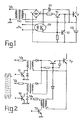
- Figure 1 shows an example of a control circuit of a power transistor Tp.
- the power supply of this circuit is done through a galvanic isolation transformer TR1 receiving an alternating current at 50 Hz or at higher frequency (20 kilohertz for example).
- the secondary of the transformer TR is a winding having a midpoint connected to the emitter of the transistor Tp.
- the voltage across the rectifier is rectified by a diode bridge and filtered by two capacitors C1 and C2.
- the actual control circuit consists of two transistors TI and T2, the emitters of which are connected to the base of the power transistor Tp.
- the transistors Tl and T2 are controlled by the output of an optoelectronic coupler CO receiving an all-or-nothing control signal and ensuring the transmission of this signal with galvanic isolation.
- the transistor TI is made conductive by this signal, the transistor T2 is blocked and the base of the transistor Tp receives a positive current which makes this transistor conductive.
- T2 When T1 is blocked, T2 is made conductive and a negative current is extracted from the base of the transistor Tp which is therefore blocked.
- the optoelectronic coupler is replaced by a small transformer driven in short positive and negative pulses and followed by a flip-flop; the speed of transmission of the control signal is greater but the sensitivity to parasites is also greater and its effect is even more annoying because of the flip-flop which can maintain an incorrect state for a long time (memorization of the imposed state by a parasite).
- FIG. 2 Another type of control circuit is shown in FIG. 2. It has the advantage of being very insensitive to interference but it has the drawback of requiring three transformers for each transistor to be switched; on the other hand, it does not make it possible to maintain a negative bias on the base of the transistor Tp when the latter is blocked.
- This diagram works as follows: three transistors TI, T2, T3 each control a primary transformer winding. TI and T2 are switched on alternately (at a high frequency) while T3 is blocked; the transistor Tp then receives a positive base current alternately from the transformers controlled by TI and T2 respectively. Tp is therefore conductive.
- T3 To block Tp, we make T3 conductive for a short time, at the same time as we block TI and T2. A temporary negative base current is then extracted from the base of Tp which is blocked.
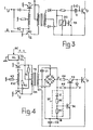
- FIG. 3 Another known control circuit diagram is shown in FIG. 3. This diagram uses only one transformer used to transmit both the energy required for the control circuit and the conduction and blocking control signal from the power transistor Tp.
- the transformer TR has a primary winding and two secondary windings, one of which is coupled to the primary with two transistors TI and T2 to constitute an oscillator, and the other of which is galvanically isolated from the primary to supply the basic control circuit properly said.
- the oscillator can be started or blocked from two inputs acting on the bases of the TI and T2 transistors.
- an oscillating signal is received or not received depending on whether or not the oscillator oscillates on the primary side.
- the secondary oscillating signal when it exists, establishes a positive base current making the transistor Tp conductive.
- a threshold detector DS detects this disappearance and momentarily conducts a transistor T3 which extracts a negative current from the base of the transistor Tp, with the help of a capacitor C which had charged during the conduction of the transistor Tp.
- the present invention provides a control circuit which makes it possible to best resolve all of the problems encountered in known circuits.
- the control circuit intended to ensure the switching of a power semiconductor component as a function of the binary state of a switching control signal, with galvanic isolation between this control signal and the component, comprises a transformer having a primary winding and at least one secondary winding, an oscillator supplied by a DC voltage and providing an oscillating signal to the primary winding, a rectifier bridge at the output of the secondary winding, and a transistor circuit supplied by the rectifier bridge and providing to a power component control electrode either a conduction current of the power component, or a blocking current, depending on the control signal.
- the secondary winding is in principle a mid-point winding, this point defining a reference potential and the rectifier bridge providing positive and negative voltages for the supply of the transistor circuit.
- the semiconductor component whose switching is to be ensured is a power transistor Tp, of the NPN type.
- the circuit controlled by this transistor is not shown. Only the transistor control circuit is shown.
- the control is carried out by a binary control signal SC having two possible states, one establishing the conduction of the transistor Tp, the other establishing its blocking.
- the primary winding EPI there is a primary winding EPI, a main secondary winding ES and an auxiliary secondary winding ES2.
- the primary winding EP1 and the auxiliary secondary winding ES2 are located galvanically on the side of the control signal SC.
- the main secondary winding ES1 is located galvanically on the side of the power transistor and the intermediate tap of this winding is moreover connected directly to the emitter of the power transistor; the potential of this emitter defines a reference with respect to which it will be seen that the base of the transistor Tp can be positively or negatively biased.
- the primary winding EP of the transformer receives alternating electrical energy from an oscillating circuit constituted in a conventional manner (which is essentially found in Figure 3) from two transistors T1 and T2, from the primary winding EP 1 itself and the auxiliary secondary winding ES2.
- This oscillating circuit is constituted in the following way: the transistors have their emitter connected to a ground (ground on the side of the control signal), have their collector respectively connected to one end of the primary winding, and have their base connected respec - tivment each at one end of the auxiliary winding; a resistor R 1 connects the collector of transistor Tl to the base of transistor T2; a resistor R2 connects the collector of transistor T2 at the base of transistor Tl; a resistor R3 connects the intermediate (middle) tap of the winding ES2 to the ground. Finally, a direct supply voltage is applied to the intermediate (middle) tap of the primary winding EP 1.
- the diagram of Figure 4 differs from that of Figure 3 (for the part which is located galvanically on the side of the control signal) on two aspects: the first is the fact that there is not in Figure 4 control terminals connected to the bases of the transistors to establish or stop the oscillation of the oscillator; the oscillator always oscillates; ie the second is the fact that the supply voltage in FIG. 4 does not come from a fixed bias source but comes from a supply AL controlled by the control signal SC and capable of supplying, according to the state of this signal, two supply voltages of different non-zero values Va and Vb (of the same sign obviously, corresponding to the type of tansistors T and T2: positive sign for NPN transistors).
- the voltages Va and Vb are both sufficient to ensure on the one hand a stable oscillation of the oscillator (at a frequency of a few tens of kilohertz so that the transformer TR remains small) and on the other hand a transmission of sufficient energy through the main secondary winding ES1, so that the circuit supplied by this secondary operates normally and allows adequate positive or negative polarization of the base of the transistor Tp both when the supply voltage is set to Va and when 'it has the value Vb.
- rectifier bridge RD On the side which is galvanically connected to the transistor Tp, there is a rectifier bridge RD with four diodes arranged at the terminals of the main secondary winding ES1, and filtering capacitors of small value, respectively CI and C2, between each output of the rectifier bridge RD and the center tap of the secondary winding.
- the rectifier bridge Compared to the reference potential defined by this center tap and applied to the emitter of the power transistor, the rectifier bridge therefore supplies rectified and filtered supply voltages, positive and negative (in principle symmetrical).
- the positive output terminal is designated by the letter A, the negative terminal by the letter B.
- a voltage level detector DT is placed between terminals A and B to indicate whether the rectified voltage supplied by the bridge corresponds to a primary supply by the voltage Va or on the contrary to a primary supply by the voltage Vb.
- This voltage level detector controls a circuit with two transistors T3 and T4, connected to the base of the transistor Tp, to cause this circuit to establish a positive base current, ensuring the conduction and the conduction maintenance of the transistor Tp, when the detected voltage corresponds to a supply Va, and to establish on the contrary a negative base current, ensuring not only an extraction of base current necessary for blocking the transistor Tp, but also the maintenance of a negative base bias originating of terminal B, when the detected voltage corresponds to a supply Vb.
- the transistor circuit thus controlled is very simple: it comprises a transistor T3 having its emitter connected to the base of the power transistor, its collector connected through a limiting resistor R4 to the positive output terminal A of the rectifier bridge, and its base connected by a bias resistor R5 to this terminal A.
- a diode D is mounted in antiparallel across the terminals of the base-emitter junction of the transistor T3, that is to say that for an NPN transistor the anode of the diode is connected to the emitter and its cathode to the base.
- a transistor T4 has its base connected to the output of the detector level DT, its emitter connected to terminal B and its collector connected to the base of transistor T3.
- the voltage level detector can also be very simple: it comprises in FIG. 4 a zener diode Z in series with a bridge of current limiting resistors R6, R7, the whole connected between the terminals A and B, the output of the detector being taken at the junction point of resistors R6 and R7.
- the zener diode When the primary is supplied with the voltage Va, the zener diode remains blocked, the supply voltage between the terminals A and B being lower than the nominal voltage of this diode.
- the transistor T4 remains blocked because its base receives no current; the transistor T3 is on the contrary normally polarized and supplies from terminal A a positive basic current maintaining the transistor Tp conductive.
- the zener diode When the primary power is supplied with the voltage Vb, the zener diode is conducting because the voltage between the terminals A and B is now greater than its nominal voltage; transistor T4 becomes highly conductive, its collector goes to the potential of terminal B (negative), which has the effect of firstly lowering the potential of the base of transistor T3 below the potential of its emitter and therefore to block it, and on the other hand to extract a negative current from the base of the transistor Tp through the diode D, extraction which is necessary to ensure rapid blocking of the transistor Tp.
- the conductive transistor T4 maintains a negative bias of the base of the transistor Tp until the control signal SC changes state and reduces the primary supply voltage to Va.
- the circuit which has just been described is entirely applicable to the control of other semiconductor elements and more particularly to the control of thyristors lockable by the trigger.
Landscapes
- Engineering & Computer Science (AREA)
- Power Engineering (AREA)
- Dc-Dc Converters (AREA)
Applications Claiming Priority (2)
| Application Number | Priority Date | Filing Date | Title |
|---|---|---|---|
| FR8408848 | 1984-06-06 | ||
| FR8408848A FR2565744B1 (fr) | 1984-06-06 | 1984-06-06 | Circuit de commande de commutation avec isolement galvanique et durees de conduction variables de zero a l'infini |
Publications (2)
| Publication Number | Publication Date |
|---|---|
| EP0167431A1 true EP0167431A1 (de) | 1986-01-08 |
| EP0167431B1 EP0167431B1 (de) | 1987-09-02 |
Family
ID=9304758
Family Applications (1)
| Application Number | Title | Priority Date | Filing Date |
|---|---|---|---|
| EP19850401094 Expired EP0167431B1 (de) | 1984-06-06 | 1985-06-04 | Schaltung zur Steuerung von Schaltvorgängen mit galvanischer Trennung und variabler Zeitdauer von Null bis Unendlich |
Country Status (3)
| Country | Link |
|---|---|
| EP (1) | EP0167431B1 (de) |
| DE (1) | DE3560546D1 (de) |
| FR (1) | FR2565744B1 (de) |
Cited By (4)
| Publication number | Priority date | Publication date | Assignee | Title |
|---|---|---|---|---|
| EP0262017A1 (de) * | 1986-09-15 | 1988-03-30 | Merlin Gerin | Basissteuerschaltung für Transistoren eines Wechselrichterzweiges |
| EP0286205A3 (en) * | 1987-02-09 | 1989-11-29 | Westinghouse Electric Corporation | Power transistor drive circuit |
| US20100064705A1 (en) * | 2008-09-16 | 2010-03-18 | Sauermann Industrie | Device for controlling a condensate lift pump, and corresponding capacitive detector and system |
| CN103595226A (zh) * | 2013-10-30 | 2014-02-19 | 安徽动力源科技有限公司 | 变压器隔离对称互补驱动电路 |
Families Citing this family (1)
| Publication number | Priority date | Publication date | Assignee | Title |
|---|---|---|---|---|
| DE3836950C3 (de) * | 1988-10-29 | 1997-09-04 | Frankl & Kirchner | Schaltungsanordnung zur Ansteuerung eines bürstenlosen, dreisträngigen Gleichstrommotors zum Antrieb von Industrie-Nähmaschinen |
Citations (2)
| Publication number | Priority date | Publication date | Assignee | Title |
|---|---|---|---|---|
| FR2335051A1 (fr) * | 1975-12-08 | 1977-07-08 | Nixdorf Computer Ag | Dispositif de circuit pour reduire la puissance dissipee a la coupure d'un transistor de commutation, et pour accelerer son passage a l'etat conducteur |
| GB2095943A (en) * | 1981-04-01 | 1982-10-06 | Lucas Industries Ltd | Transistor drive circuit |
-
1984
- 1984-06-06 FR FR8408848A patent/FR2565744B1/fr not_active Expired
-
1985
- 1985-06-04 EP EP19850401094 patent/EP0167431B1/de not_active Expired
- 1985-06-04 DE DE8585401094T patent/DE3560546D1/de not_active Expired
Patent Citations (2)
| Publication number | Priority date | Publication date | Assignee | Title |
|---|---|---|---|---|
| FR2335051A1 (fr) * | 1975-12-08 | 1977-07-08 | Nixdorf Computer Ag | Dispositif de circuit pour reduire la puissance dissipee a la coupure d'un transistor de commutation, et pour accelerer son passage a l'etat conducteur |
| GB2095943A (en) * | 1981-04-01 | 1982-10-06 | Lucas Industries Ltd | Transistor drive circuit |
Cited By (6)
| Publication number | Priority date | Publication date | Assignee | Title |
|---|---|---|---|---|
| EP0262017A1 (de) * | 1986-09-15 | 1988-03-30 | Merlin Gerin | Basissteuerschaltung für Transistoren eines Wechselrichterzweiges |
| EP0286205A3 (en) * | 1987-02-09 | 1989-11-29 | Westinghouse Electric Corporation | Power transistor drive circuit |
| US20100064705A1 (en) * | 2008-09-16 | 2010-03-18 | Sauermann Industrie | Device for controlling a condensate lift pump, and corresponding capacitive detector and system |
| US8397525B2 (en) * | 2008-09-16 | 2013-03-19 | Sauermann Industrie | Device for controlling a condensate lift pump, and corresponding capacitive detector and system |
| CN103595226A (zh) * | 2013-10-30 | 2014-02-19 | 安徽动力源科技有限公司 | 变压器隔离对称互补驱动电路 |
| CN103595226B (zh) * | 2013-10-30 | 2016-03-16 | 安徽动力源科技有限公司 | 变压器隔离对称互补驱动电路 |
Also Published As
| Publication number | Publication date |
|---|---|
| FR2565744A1 (fr) | 1985-12-13 |
| EP0167431B1 (de) | 1987-09-02 |
| FR2565744B1 (fr) | 1986-08-29 |
| DE3560546D1 (en) | 1987-10-08 |
Similar Documents
| Publication | Publication Date | Title |
|---|---|---|
| EP0002983B1 (de) | Leistungssteuerkreis und seine Anwendung in einer pulsierenden Spannungsspeiseeinrichtung | |
| EP0680245B1 (de) | Statischer Wandler mit gesteuertem Schalter und Steuerungsschaltung | |
| EP0082071B1 (de) | Einrichtung für die Umschaltung einer mit mindestens einem gesteuerten Schalter versehenen Gleichspannungsquelle und Kommutierungshilfsschaltung für eine solche Einrichtung | |
| EP0041883A1 (de) | Geschaltete Speisespannungseinrichtung mit geregeltem Anschnitt, kombiniert mit der Zeilenablenkschaltung eines Fernsehempfängers, welchen sie speist | |
| FR2795283A1 (fr) | Circuit d'allumage de lampe a decharge pour une pluralite de lampes | |
| EP3745578B1 (de) | Entladung eines wechselkondensators | |
| EP0167431B1 (de) | Schaltung zur Steuerung von Schaltvorgängen mit galvanischer Trennung und variabler Zeitdauer von Null bis Unendlich | |
| FR2610149A1 (fr) | Convertisseur continu-continu a rendement eleve a faible charge | |
| EP0043761B1 (de) | Schalttransistorsteuerschaltung in einem statischen Wandler und Wandler mit dieser Schaltung | |
| EP0022380B1 (de) | Mit einer Zeilenablenkschaltung eines Fernsehempfängers kombinierter Sperrwandler zur Erzeugung einer Betriebsspannung, der mittels variabler Phasenverschiebung geregelt wird | |
| EP0029627A1 (de) | Vorrichtung zum Erkennen des Schleifenschlusses einer Teilnehmerleitung während des Klingelns | |
| FR2581488A1 (fr) | Perfectionnement aux alimentations en courant alternatif non susceptibles d'etre interrompues | |
| EP0370896B1 (de) | Leistungs-Schalteinrichtung, insbesondere für Umrichter | |
| EP1142095B1 (de) | Leistungsübertragungsvorrichtung mit elektrischer energieumwandlung | |
| EP0087541B1 (de) | Stromversorgungsschaltung und eine Übertragungsvorrichtung mit dieser Schaltung | |
| FR2601209A1 (fr) | Circuit de pilotage de base pour transistor | |
| FR2479590A1 (fr) | Circuit de protection a reponse rapide pour transistor de puissance, et dispositif d'alimentation electrique a decoupage comportant un tel circuit | |
| EP0165640B1 (de) | Vorrichtung zur galvanischen Isolierung zwischen einem Impulsgeber und einer Belastung | |
| FR2851379A1 (fr) | Convertisseur en transfert direct d'energie | |
| FR2520958A1 (fr) | Circuit auxiliaire pour televiseur | |
| EP1177613B1 (de) | Telefonleitungsgespeistes stromversorgungssystem | |
| EP0200600A1 (de) | Bei hoher Frequenz arbeitende Transistorbasissteuerschaltung | |
| EP0012634B1 (de) | Spannungsregelvorrichtung, insbesondere für tragbaren Fernsehempfänger | |
| FR2808631A1 (fr) | Dispositif d'entree logique pour automate | |
| EP1324478A2 (de) | Hochspannungswandler mit schneller Antwortzeit |
Legal Events
| Date | Code | Title | Description |
|---|---|---|---|
| PUAI | Public reference made under article 153(3) epc to a published international application that has entered the european phase |
Free format text: ORIGINAL CODE: 0009012 |
|
| AK | Designated contracting states |
Designated state(s): DE FR GB IT NL |
|
| 17P | Request for examination filed |
Effective date: 19860117 |
|
| 17Q | First examination report despatched |
Effective date: 19861027 |
|
| GRAA | (expected) grant |
Free format text: ORIGINAL CODE: 0009210 |
|
| AK | Designated contracting states |
Kind code of ref document: B1 Designated state(s): DE FR GB IT NL |
|
| ITF | It: translation for a ep patent filed | ||
| REF | Corresponds to: |
Ref document number: 3560546 Country of ref document: DE Date of ref document: 19871008 |
|
| GBT | Gb: translation of ep patent filed (gb section 77(6)(a)/1977) | ||
| PLBE | No opposition filed within time limit |
Free format text: ORIGINAL CODE: 0009261 |
|
| STAA | Information on the status of an ep patent application or granted ep patent |
Free format text: STATUS: NO OPPOSITION FILED WITHIN TIME LIMIT |
|
| 26N | No opposition filed | ||
| PGFP | Annual fee paid to national office [announced via postgrant information from national office to epo] |
Ref country code: NL Payment date: 19900630 Year of fee payment: 6 |
|
| ITTA | It: last paid annual fee | ||
| PG25 | Lapsed in a contracting state [announced via postgrant information from national office to epo] |
Ref country code: NL Effective date: 19920101 |
|
| NLV4 | Nl: lapsed or anulled due to non-payment of the annual fee | ||
| REG | Reference to a national code |
Ref country code: FR Ref legal event code: D6 |
|
| PGFP | Annual fee paid to national office [announced via postgrant information from national office to epo] |
Ref country code: GB Payment date: 20000531 Year of fee payment: 16 |
|
| PGFP | Annual fee paid to national office [announced via postgrant information from national office to epo] |
Ref country code: DE Payment date: 20000605 Year of fee payment: 16 |
|
| PGFP | Annual fee paid to national office [announced via postgrant information from national office to epo] |
Ref country code: FR Payment date: 20000612 Year of fee payment: 16 |
|
| PG25 | Lapsed in a contracting state [announced via postgrant information from national office to epo] |
Ref country code: GB Free format text: LAPSE BECAUSE OF NON-PAYMENT OF DUE FEES Effective date: 20010604 |
|
| GBPC | Gb: european patent ceased through non-payment of renewal fee |
Effective date: 20010604 |
|
| PG25 | Lapsed in a contracting state [announced via postgrant information from national office to epo] |
Ref country code: FR Free format text: LAPSE BECAUSE OF NON-PAYMENT OF DUE FEES Effective date: 20020228 |
|
| PG25 | Lapsed in a contracting state [announced via postgrant information from national office to epo] |
Ref country code: DE Free format text: LAPSE BECAUSE OF NON-PAYMENT OF DUE FEES Effective date: 20020403 |
|
| REG | Reference to a national code |
Ref country code: FR Ref legal event code: CD |